background image

– 5 –

6

Using Your New TV

VIDEO 3 INPUT

(MONO)

AUDIO

VIDEO

S1 VIDEO

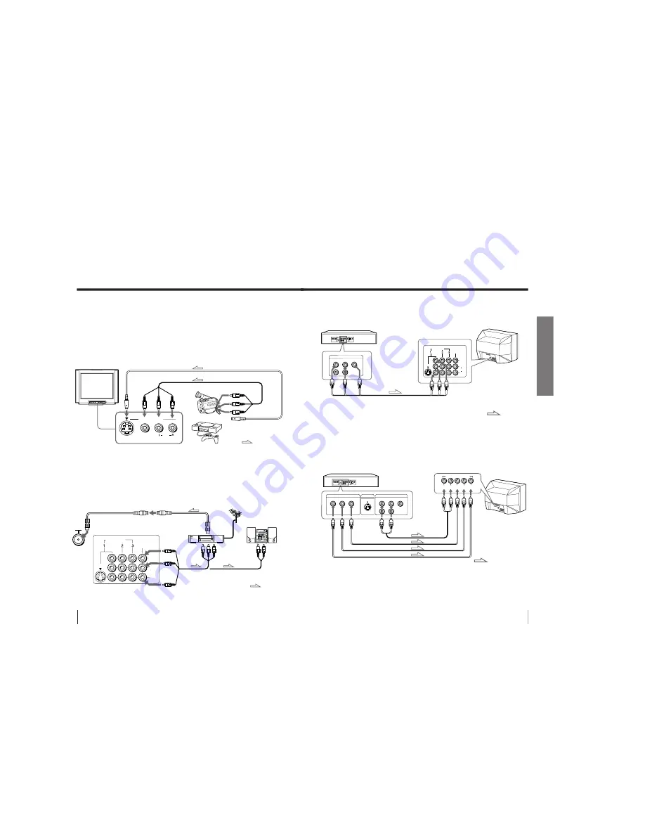
Connecting optional components

You can connect optional audio/video components, such as a VCR, multi disc player,
camcorder, video game or stereo system. If you connect a cable box, contact your
CATV provider.

Connecting a camcorder/video game equipment
using the VIDEO 3 INPUT jacks

Notes

• You can also connect video equipment to the VIDEO IN 3 jacks at the rear

of your TV.

• Do not simultaneously connect video equipment to the VIDEO 3 INPUT

jacks at the front and the VIDEO IN 3 jacks at the rear of your TV;
otherwise, the picture will not be displayed properly on the screen.

Connecting audio/video equipment using the
MON/TV OUT jacks

Note

• When connecting a monaural VCR, connect the yellow plug to VIDEO (the yellow

jack) and the black plug to AUDIO -L (MONO) (the white jack).

To  S video output

Front of TV

Camcorder

Video game
equipment

To video and
audio outputs

VIDEO (yellow)
AUDIO-L
(MONO) (white)
AUDIO-R (red)

Rear of TV

To
antenna
output

To video and
audio inputs

or

Audio system

To
audio
inputs

VCR

:Signal flow

:Signal flow

To
S1 VIDEO

To VIDEO 3
INPUT

To MON/TV
(monitor/
TV) OUT

or

Audio/Video cable (not supplied)

S video cable (not supplied)

Antenna cable (not supplied)

Audio/Video cable
(not supplied)

Antenna cable (supplied)

VIDEO IN

MON/TV

OUT

VIDEO

L

(MONO)

AUDIO
R

S1 VIDEO

7

Using Your New TV

Using Y

our New TV

Connecting a DVD player

Using the AUDIO/VIDEO connectors, connect VIDEO IN 1 on your TV to LINE OUT
on your DVD player.

Connecting a DVD player with component video output
connectors

1 Using audio connectors, connect L and R of COMPONENT VIDEO (DVD) IN on

your TV to the AUDIO L and R output connectors on your DVD player.

2 Using three yellow video cables, connect Y, C

B

, and C

R

 of COMPONENT VIDEO

(DVD) IN on your TV to Y, C

B

, and C

R

 output on your DVD player.

Notes

• Some DVD player terminals may be labeled Y, B-Y, and R-Y. If so, connect

Y (green) to Y, C

B

 (blue) to B-Y, and C

R

 (red) to R-Y.

• Since the high quality pictures on a DVD disc contain a lot of information,

picture noise may appear. In this case, adjust the sharpness (“SHARP”) in
the VIDEO ADJUST menu. (see page 22.)

• Connect your DVD player directly to your TV. Connecting the DVD

player through other video equipment will cause unwanted picture noise.

DVD player

Audio/Video cable
(not supplied)

DVD player

To
L (white)
R (red)

Audio cable
(not supplied)

To component
video output

Video cable (not supplied)

VIDEO (yellow)
AUDIO-L (MONO) (white)
AUDIO-R (red)

To VIDEO IN 1,
2, or 3

: Signal flow

To audio
output

:Signal flow

To COMPONENT
VIDEO (DVD) IN

VIDEO IN

MON/TV

OUT

VIDEO

L

(MONO)

AUDIO
R

S1 VIDEO

VIDEO 

R-AUDIO-L

LINE  OUT

VIDEO 

R-AUDIO-L

LINE  OUT

COMPONENT VIDEO OUT

S VIDEO OUT

C

B

C

R


Y

C

B

C

R

L

R

COMPONENT VIDEO(DVD) IN

Summary of Contents for TRINITRON KV-EF29N6A

Page 1: ... it s detail is displayed Date SUP COR No Description of SUP COR Change of main text 1998 05 COR 1 Change of Power Cord P94 P121 Yes 1998 05 COR 2 Change of Parts L802 P80 116 Yes Model Name KV EF29N6A N6B N9P Part No 9 965 209 01 ...

Page 2: ...ER DEST CHASSIS NO MODEL COMMANDER DEST CHASSIS NO MICROFILM Please file according to model size 29 CHASSIS BG 1L TRINITRON COLOR TV KV EF29N6A RM 882 AN SCC N80A A KV EF29N6B RM 882 BRZ SCC N79A A KV EF29N9P RM 882 MX SCC N78A A ...

Page 3: ...equirements Power consumption W Color system Stereo system On screen language Channel coverage Antenna Audio output speaker Number of terminal VIDEO AUDIO S1 VIDEO COMPONENT VIDEO 2 Headphones Picture tube Tube size cm Screen size cm Dimensions w h d mm Mass kg KV EF29N6B KV EF29N6A KV EF29N9P Note 110 240 V AC 50 60 Hz 183 NTSC PAL M NTSC PAL N MTS English Spanish VHF 2 13 UHF 14 69 CATV 1 125 75...

Page 4: ...djustments with Commander 31 5 2 Adjustment Method 32 5 3 Picture Quality Adjustments 37 5 4 Display Position Adjustments 37 5 5 A Board Adjustment After IC003 MEMORY Replacement 38 TABLE OF CONTENTS 6 DIAGRAMS 6 1 Block Diagrams 39 6 2 Circuit Boards Location 52 6 3 Schematic Diagrams and Printed Wiring Boards 53 1 Schematic Diagram of A Board 57 2 Schematic Diagrams of H7 J P3 and P4 Boards 62 3...

Page 5: ...te jack If you connect a VCR to the antenna terminal preset the signal output from the VCR to the program position 0 on the TV Do not simultaneously connect video equipment to the VIDEO 3 INPUT jacks at the front and the VIDEO IN 3 jacks at the rear of your TV If both S1 VIDEO and VIDEO of VIDEO IN 1 are input simultaneously the S1 VIDEO is automatically selected To view the video input to VIDEO I...

Page 6: ...ied Antenna cable supplied VIDEO IN MON TV OUT VIDEO L MONO AUDIO R S1VIDEO 7 Using Your New TV Using Your New TV Connecting a DVD player Using the AUDIO VIDEO connectors connect VIDEO IN 1 on your TV to LINE OUT on your DVD player Connecting a DVD player with component video output connectors 1 Using audio connectors connect L and R of COMPONENT VIDEO DVD IN on your TV to the AUDIO L and R output...

Page 7: ...s can be done using the remote 1 Press MAIN POWER to turn on the TV When the TV is in the standby mode the STANDBY STEREO WAKE UP indicator on the TV is lit press POWER on the remote or POWER u on the TV The CHANNEL CH VOLUME TV VIDEO and POWER u indicators on the TV light up 2 Press CH or number buttons to select the TV program For double digit numbers press the numbers then ENTER e g for 25 pres...

Page 8: ...g Your New TV Using Your New TV To set the Wake Up timer 1 Press WAKE UP until the desired period of time appears Every time you press this button the period of time changes as follows 2 Select the TV program or video mode you want to display when you wake up 3 Press POWER on the remote or set the Sleep timer if you want the TV to turn off automatically To cancel the Wake Up timer press WAKE UP un...

Page 9: ...Operations Advanced Operations Listening with Virtual Dolby Surround sound The Virtual Dolby Surround sound mode enables you to enjoy Dolby ProLogic Surround without surround speakers Press DOLBY VIRTUAL The sound mode of the TV program or the video input changes to the Virtual Dolby Surround sound To go back to the normal sound mode Press DOLBY VIRTUAL again Manufactured under license from Dolby ...

Page 10: ...You can also select a TV program in the PIP screen using the menu see Adjusting the PIP setting on page 24 TV VIDEO FREEZE SWAP PIP b V v PIP 1 2 3 4 5 6 7 8 0 9 MUTING DISPLAY GAME POWER MTS VIDEO TV TV VIDEO FREEZE SWAP PIP DVD MENU MENU PIP CH DYNAMIC P BASSO WAKE UP SLEEP VIRTUAL DOLBY 15 Advanced Operations Additional PIP tasks To swap pictures between the main and PIP screens freeze the PIP ...

Page 11: ...ast MTS 1 2 3 4 5 6 7 8 0 9 MUTING DISPLAY GAME POWER MTS VIDEO TV TV VIDEO FREEZE SWAP PIP DVD MENU MENU 17 Advanced Operations Viewing a video game screen GAME MODE The GAME MODE feature optimizes the video game screen by giving a soft picture and dynamic sound effects Press GAME The picture and sound change to the mode that is suitable for video games To go back to the normal picture and sound ...

Page 12: ...ld down VIDEO POWER and press 00 01 02 03 04 06 07 VIDEO POWER 0 2 POWER VIDEO 1 2 3 4 5 6 7 8 0 9 TV VIDEO FREEZE SWAP PIP DVD MENU MENU PIP CH DYNAMIC P BASSO WAKE UP SLEEP VIRTUAL DOLBY VOL CH POWER VIDEO TITLE 19 Advanced Operations Operating a VCR using the remote Operating a DVD player using the remote Operating an MDP using the remote To turn on off record play stop fast forward rewind the ...

Page 13: ...GRAM L ANGUAGE I D I O M A GAME MODE HYPER SURROUND OF F MON I TOR AV OUT FEATURES P I CTURE 4 0 1 0 0 0 8 0 V I DEO ADJUST COLOR BR I GHT HUE SHARP VM HIGH 4 5 0 BASS 8 0 0 0 8 0 TREBLE BALANCE AUD I O ADJUST P I P P I P OFF POS I T I ON 7 8 0 9 TV VIDEO FREEZE SWAP PIP DVD MENU MENU PIP CH DYNAMIC P BASSO WAKE UP SLEEP VIRTUAL DOLBY VOL CH 1 AUTO PROGRAM ERASE ATTENUATOR OFF CHANNEL 110 ADD MANU...

Page 14: ...ZE SWAP PIP DVD MENU MENU PIP CH 23 Adjusting Your Setup MENU Adjusting the VIDEO ADJUST settings 1 Press V b v B to adjust the selected item then press You can adjust HUE for the NTSC color system only 2 Repeat the above step to adjust other items Adjusting the AUDIO ADJUST settings 1 Press V b v B to adjust the selected item then press 2 Repeat the above step to adjust other items To go back to ...

Page 15: ...IDEO FREEZE SWAP PIP DVD MENU MENU PIP CH P I P P I P OFF POS I T I ON 25 Adjusting Your Setup MENU 3 Press V or v to move the cursor to the desired option see the table below then press Tip For details on the menu system and how to use the menu see the Introducing the menu system section on page 20 Select PIP POSITION To display a sub screen within the main picture Press V b v B to select ON then...

Page 16: ...ed by Sony Corporation under license from BBE Sound Inc It is covered by U S Patent No 4 638 258 and No 4 482 866 The word BBE and the BBE symbol are the trademarks of BBE Sound Inc 2 The r SRS SOUND RETRIEVAL SYSTEM is manufactured by Sony Corporation under license from SRS Labs Inc It is covered by U S Patent No 4 748 669 The word SRS and the SRS symbol r are registered trademarks of SRS Labs In...

Page 17: ... O ADJUST T I L T CORRECT 0 PRESET MTS STEREO SYS T E M A U T O CABLE OF F ENGL I SH AUTO PROGRAM MANUA L PROGRAM L ANGUAGE I D I O M A b 1 2 3 4 5 6 7 8 0 9 MUTING DISPLAY GAME POWER MTS VIDEO TV TV VIDEO FREEZE SWAP PIP DVD MENU MENU PIP CH ERASE ATTENUATOR OFF CHANNEL 1 1 0 ADD MANUA L PROGRAM ERASE ATTENUATOR OFF CHANNEL 110 ADD MANUAL PROGRAM ERASE ATTENUATOR OFF CHANNEL 230 ADD MANUAL PROGRA...

Page 18: ...F ENGL I SH AUTO PROGRAM MANUA L PROGRAM L ANGUAGE I D I O M A 31 Additional Information Additional Information Troubleshooting If any problem persists contact your nearest Sony dealer or authorized service center Dotted lines or stripes Double images or ghosts No picture No sound No color Noisy sound Snowy picture Good picture No sound Additional Information continued Symptom Check Check the ante...

Page 19: ...cted page 16 TV cabinet creaks Troubleshooting continued No sound when SAP is selected 33 Additional Information Identifying parts and controls Refer to the pages indicated in parentheses for details Front panel 1 TV VIDEO button 10 2 VOLUME Á buttons 10 3 CHANNEL CH buttons 9 4 POWER u button 9 5 ENTER button 20 6 MENU buttons 20 7 AUTO PROGR program button 5 8 MAIN POWER button 9 continued ONE P...

Page 20: ...VIDEO TV TV VIDEO FREEZE SWAP PIP DVD MENU MENU PIP CH DYNAMIC P BASSO WAKE UP SLEEP VIRTUAL DOLBY VOL CH POWER VIDEO TITLE 35 Additional Information DOLBY VIRTUAL button 13 Timer setting buttons 11 WAKE UP SLEEP DYNAMIC P power BASSO button 12 VOL volume buttons 10 Button function For general TV operations For PIP operations Names symbols of buttons on the remote are indicated in different colors...

Page 21: ...VAL 2 4 SERVICE POSITION 1 Five screws BVTP 4x16 1 Six screws BVTP 4x16 2 Rear cover 5 Two tapping screws P 4x16 3 Two tapping screws P 4x16 6 Speaker Box L ass y 4 Speaker Box R ass y 1 Two screws BVTP 4x16 2 Speaker stay 1 Anode cap Refer to page 21 3 Remove the chassis ass y to direction of the arrow A 2 Claw 2 Claw A Chassis ass y ...

Page 22: ...ng called as shatter hook terminal is built in the rubber 3 Don t turn the foot of rubber over hardly The shatter hook terminal will stick out or hurt the rubber REMOVAL OF ANODE CAP NOTE Short circuit the anode of the picture tube and the anode cap to the metal chassis CRT shield or carbon painted on the CRT after removing the anode REMOVING PROCEDURES 1 Turn up one side of the rubber cap in the ...

Page 23: ...ip Demagnetic coil 0 Four claws 1 Two tapping screws P 4x16 2 Speaker box L ass y Two screws Tension spring Two screws 6 Chassis ass y 3 Two tapping screws P 4x16 4 Speaker box R ass y 9 Deflection yoke 8 Neck ass y 7 C1 board 5 Anode cap Refer to page 21 Picture tube Cushion ...

Page 24: ...CN106 CN103 CN102 CN506 CN3001 CN2821 CN0521 CN 1691 CN909 B G Connector H C A CN703 C1 board D board D2 board A5 board B3 board A board CN 704 CN902 CN901 CN 905 CN 907 CN528 CN 1690 D E DH board CN3305 CN3304 CN120 CN117 CN108 CN107 DISASSEMBLED IN THE ORDER SHOWN BELOW REAR COVER 1 Eleven screws SPEAKER BOX L R ASS Y 1 Purse lock A 2 Two connector F G 3 Four screws CHASSIS SLIDE 1 Purse lock B ...

Page 25: ...th the pattern generator Contrast Brightness 2 Position neck ass y as shown in Fig3 2 3 Set the pattern generator raster signal to a red raster 4 Move the deflection yoke to the rear and adjust with the purity control so that the red is at the center and the blue and the green take up equally sized areas on each side See Figures 3 1 through 3 3 5 Move the deflection yoke forward and adjust so that...

Page 26: ...center of the screen 3 If the H STAT variable resistor cannot bring the red green and blue points together at the center of the screen adjust the horizontal convergence with the H STAT variable resistor and the V STAT magnet in the manner given below In this case the H STAT variable resistor and the V STAT magnet influence each other Tilt the V STAT magnet and adjust the static convergence by open...

Page 27: ...orrection magnet on the neck assembly so that the horizontal lines at the top and bottom of the screen are straight Note 1 The Red and Blue magnets should be equally far from the horizontal center line 2 Do not seperate the Red and Blue magnets too far Less than 8 mm VM Board VM Board BLUE RED RED BLUE Use the H STAT VR to adjust the red green and blue dots so that they coincide at the center of s...

Page 28: ...crews 2 Remove the deflection yoke spacer 3 Move the deflection yoke as shown in the figure below and optimize the convergence 4 Tighten the deflection yoke screws 5 Install the deflection yoke spacer 3 Screen corner Convergence Affix a Permalloy assy corresponding to the misconverged areas b a d c b a d c Permalloy assembly a b screen cor ner misconvergence R G B B G R R G B B G R R G B B G R R G...

Page 29: ...3D 3E Adjustment item SBR GDR BDR GCF BCF Note SUB BRIGHTNESS G Drive B Drive G CUT OFF B CUT OFF Standard DATA 24 1D 20 07 08 FLYBACK TRANSFORMER T801 Focus b METHOD OF CANCELLATION FROM SERVICE MODE Set the standby condition Press POWER button on the commander then press POWER button again hereupon it be comes TV mode c METHOD OF WRITE FOR MEMORY 1 Set to Service Mode 2 Press 1 UP and 4 DOWN sel...

Page 30: ... BALANCE ADJUSTMENTS 1 Set to service Mode 2 Input white raster signal 3 Set the PICTURE to minimum 4 Select SBR 39 with 1 and 4 and then set the level to minimum with 3 and 6 5 Select GCF 3D and BCF 3E with 1 and 4 And adjust the level with 3 and 6 for the best white balance 6 Set the PICTURE to maximum 7 Select GDR 3B and BDR 3C with 1 and 4 and adjust the level with 3 and 6 for the best white b...

Page 31: ...equency responding to each failed device is shown below Board name Ref No Device Flickering Frequency A Board IC1201 AV SWITCH CXA1855S 2 A Board IC104 MAIN Y C CXA2050S 3 A Board IC206 SURROUND PROCESSOR TDA8424 6 All the devices are checked one after another from the left on the table If an error is found the responding LED will start flickering So if more than 2 devices are failed the one on th...

Page 32: ... writing 7 0 All the data becomes the values in memory 8 0 All user control goes to the standard state 5 0 Service data initialization Be sure not to use usually 2 0 Write 50Hz adjustment data to 60Hz or vice versa The screen display is RM 882 Depends on the signals PAL N 50 NTSC PAL M 60 00 VSH 1F SERVICE 50 XXX 00 00 00 20 V2 1C DATA Mode Adjstment item Item number SOFTWAR VERSION H SYNC COUNTER...

Page 33: ...me method for Items Number 00 99 Use 1 and 4 to select the adjustment item use 3 and 6 to adjust write with MUTING then execute the write with Note In WRITE the data of all items are into memory As for V FREQ by searching the bolded screen V range with adjusting data Note For adjustment Items that have differnt standard data between 50Hz or 60Hz and novwel or wid be sure to use the respective inpu...

Page 34: ...N OFF 13 LBK 00 0F 0F L BLK WIDTH 14 RBK 00 0F 0F R BLK WIDTH 15 JSW 00 01 00 JUMP ON OFF SW 16 VBW 00 03 02 V BLK WID CON 17 AFC 00 03 01 AFC MODE 03 18 FHH 00 01 00 FH HI 19 VFQ 00 03 00 V FREQ 1A VOF 00 01 00 V OFF 1B VMD 00 01 00 CD MODE2 1C CMD 00 01 00 CD MODE 1D TTL 00 03 00 INTERLACE 1E ZSW 00 01 00 ZOOM SW 1F POV 00 03 03 PRE OVER 20 CT1 00 01 01 C TRAP NTSC 21 CT2 00 01 01 C TRAP PAL 22 ...

Page 35: ... ON OFF 47 ABL 00 01 00 ABL PIC PICandBRT SW 1 PIC ONLY 48 LIM 00 01 00 RGB LIMIT ON OFF 1 ON 49 PB 00 01 01 PICTURE BOOSTER TDA9170 4A BOF 00 01 00 BLACK OFFSET 4B UVG 00 3F 1F USER VAR GAMMA 4C ADG 00 3F 1F ADAPTIVE GAMMA 4D NLA 00 3F 05 NON LINEAR AMP 4E WDS 00 02 00 WINDOW SELECT 4F LST 00 0F 07 WINDOW LINE START 50 LSP 00 0F 07 WINDOW LINE STOP 51 FST 00 0F 07 WINDOW FIELD START 52 FSP 00 0F ...

Page 36: ...STREAM CONTROL 70 DAN 00 01 00 DAC CONTROL 87 BB1 00 3F 1D BBE CONTROL HIGH CXA1315 88 BB2 00 3F 1D BBE CONTROL MIDDLE 89 BB3 00 3F 28 BBE CONTROL LOW 8A ATW 00 03 00 AUTO WIDE IDENTSPEED CXP5068 8B BKP 00 FF 00 BLK OFF PICTURE CXP85340 8C OSH 00 3F 0D OSD POSITION H 8D ODL 00 FF 10 POWER ON DELAY 8E BLU 00 01 01 BLUE BACK ON OFF 8F ROC 00 0F 0F N S CENTER VOL 90 ROS 00 07 07 USER SET UP 91 DKS 00...

Page 37: ...M N SYS 0 0 1 1 1 1 0 1 ITEM INFORMATION 50 50Hz data 60 60Hz data Standard data listed on the Adjustment Item Table are reference values therefore if is different for every mode 99 OP1 Comb type 0 Glass comb filter 1 Digital comb filter Wide 0 4 3 model 1 16 9 model N SYS 0 M SYSTEM 1 N SYSTEM ...

Page 38: ...d 4 of the commander then adjust to VB2 VB3 VB4 with 3 and 6 5 Press MUTING of the commander to write the data 6 Adjust 36 SC2 as step 2 to 5 when receiving NTSC color bar 7 Set service item 4D NLA to data 05 and write the data SUB HUE ADJUSTMENT SH2 1 Select Video 1 2 Input a NTSC color bar video into video 1 3 Set the following condition PICTURE 100 BRIGHTNESS 50 COLOR 50 4 Connect an oscillosco...

Page 39: ...ure In cases where items are not well adjusted rectify the items with fine adjustment Write the data per each item nubmer MUTING 4 Select item numbers 98 OP0 and 99 OP1 and respectively set the bit per model with commander buttons 3 and 6 5 Press commander buttons 8 and Test Normal to return to the data that was set on the shipment from the factory This will also cancel Service Mode 5 6 PICTURE DI...

Page 40: ...OL CLAMP Q600 10 11 15 17 18 16 12 13 14 T601 F TO C1 BOARD CN701 H1 4 CN0521 7V 14V 11V AUDIO 30V IC603 ISOLATION 1 2 IC602 SENSOR AMP STBY SW Q601 603 B 56V 1 2 STBY DEGAUSS CN528 1 2 1 2 MUTE CN2603 CN3802 MUTE CN106 A D H V POWER SUPPLY 4 5 2 4 1 HV 13 7 9 11 2 4 8 10 2 4 8 10 200V B 15V T801 FBT DF 1 DF 2 FBP V BLK CN0522 CN2822 HV TO CRT DY 3 4 7 6 2 8 IN1 IN1 IN2 IN2 OUT1 OUT2 IC3805 N S DR...

Page 41: ...RI0 EBCI0 SDI0 IC3004 RESET S3 S2 S1 IC3007 AD DA CONTROL IC3002 DOLBY PROCESS IC3005 AMP IN IN OUT OUT 9V 5V IC303 5V REG A5 AUDIO PROCESS 3 2 8 9 9 8 2 3 L R SDAT SCLK CN3001 CN2203 2 2 6 27 15 18 17 16 IC2208 AUDIO PROCESS DEF SW INPUT INPUT OUTPUT OUTPUT 10 7 SW DAC0 SW3 14 15 SDAT SCLK 6 IC2201 D A CONV 10 11 3 2 10 11 2 3 L R SDAT SCLK CN2201 CN121 11 12 1 3 SCL SDA 13 9 IC206 AUDIO PROCESS ...

Page 42: ...VBS IN C A AMP BUFF Q1401 1402 1404 IC1402 DELAY LINE IC1401 3C DEC X1401 X1402 9 10 15 14 SW2 SCL SDA SW3 IC1413 D A CONV SW3 TO P3 BOARD 1 2 INV Q1408 BUFF Q1407 19 23 21 11 8 7 2 1 12 15 UV0 UV3 Y0 Y5 BLN LL3 V IN Y IN U B Y ISC Q1416 COMPARATOR BUFF Q1403 1 21 24 25 30 32 20 IC1406 A D CONV IC1407 PIP PROCESS 8 9 10 14 15 16 19 17 OUT R Y OUT Y OUT B Y SEL HSP UV0 UV3 Y0 Y5 BLNI LL3I VSI VSP S...

Page 43: ... earth chassis All voltages are in V Readings are taken with a 10 M digital multimeter Readings are taken with a color bar signal input Voltage variations may be noted due to normal production tolerances Can not be measured NO MARK PAL SECAM NTSC 3 58 MHz Circled numbers are waveform references s B bus S B bus Signal path Reference information RESISTOR RN METAL FILM RC SOLID FPRD NONFLAMMABLE CARB...

Page 44: ...1 CH CHIP 0 001 CH CHIP 220p CH CHIP 0 001 CH CHIP 100p CH CHIP 100p CH CHIP 220p CH CHIP 220p CH CHIP 0 022 B CHIP 220p CH CHIP 0 001 B CHIP 220p CH CHIP 0 1 25V B CHIP 100p CHIP 100p CH CHIP 100p CHIP 0 CHIP 100p CHIP 100p CHIP 100p CHIP 100p CHIP 100p CHIP 0 1 25V B CHIP 0 01 B CHIP 0 0015 B CHIP 220p B CHIP 0 022 B CHIP 220p CH CHIP 220p CH CHIP 220p CH CHIP 220p CH CHIP 220p CH CHIP 220p B CH...

Page 45: ...1412 R1409 R1411 R1413 R1417 R1427 R1426 R1418 R1454 R1455 R1462 R1464 R1476 R1477 R1478 R1480 R1446 C1418 C1401 C1470 C1412 C1414 C1417 C1428 C1431 C1450 C1455 C1457 C1459 C1465 C1468 C1473 C1475 C1407 C1408 C1472 C1426 C1443 C1442 C1410 C1437 C1456 R1487 FL1401 C1488 C1489 R1414 L1401 R1463 C1438 R1430 R1436 R1437 C1419 C1480 R1458 R1479 C1481 R1631 R1632 C1409 R1433 R1435 L1404 L1405 L1406 L140...

Page 46: ...C1413 B 3 IC1414 B 2 TRANSISTOR Q1401 B 2 2 Q1402 B 3 1 Q1403 B 3 2 Q1404 B 2 2 Q1405 D 3 1 Q1406 D 3 1 Q1407 D 2 1 Q1408 D 2 1 Q1409 D 3 1 Q1410 D 3 1 Q1411 D 3 1 Q1412 C 3 2 Q1413 C 3 2 Q1414 C 2 2 Q1415 C 2 2 Q1416 C 1 1 Q1418 A 3 1 Conductor Side Refer to Terminal name of semiconductors in silk screen printed circuit see page 53 Q1419 A 3 2 Q1421 A 2 2 Q1422 A 2 1 Q1423 A 3 2 Q1424 A 2 1 Q1425...

Page 47: ...ors in silk screen printed circuit 1 4 Refer to Terminal name of semiconductors in silk screen printed circuit see page 53 Ref Q3301 Q3302 Q3304 Q3310 Q3312 Q3320 D3301 D3302 c1 RGB OUTPUT NOTE The circuit indicated as left contains high voltage of over 600 Vp p Care must be paid to prevent an electric shock in inspection or repairing VM BOARD vm VOLOCITY MODULATION C1 BOARD ...

Page 48: ...EL0606 6 8µH EL0606 22µH EL0606 22µH EL0606 220 CHIP 220 CHIP 470 CHIP 470 CHIP 470 CHIP 470 CHIP 4 7k CHIP 3 9k CHIP 47k CHIP 3 9k CHIP 5 6k CHIP 12k CHIP 330 CHIP 150 CHIP 5 6k CHIP 150 CHIP 10k CHIP 100 CHIP 1k CHIP 680 CHIP 270 CHIP 3 3k CHIP 560 CHIP 5 6k CHIP 330 CHIP 39k CHIP 39k CHIP 3 3k CHIP 6 8k CHIP 560k CHIP 3 9k CHIP 0 CHIP 1k CHIP 22k CHIP 22k CHIP 22k CHIP 0 33 25V F CHIP 7 5k RN C...

Page 49: ...03 FB604 FB605 R615 C631 R2528 C808 C630 Q2600 R2604 R2607 C2618 D2604 IC601 C2604 R2601 C622 C2602 T2601 T2603 CN2605 CN2602 CN2600 JW2511 C2543 JW2522 R2556 C2545 R2557 C2514 C2507 C2561 Q2505 Q2503 R2566 R2561 R2570 R2571 Q1800 R1801 R1508 CN526 CN0523 CN506 R1501 C1518 R895 R898 R894 C875 C877 D825 D824 D1502 Q1503 D1508 C1520 R1520 R1518 R1519 C629 FB609 R2530 R2531 R2524 R2583 JW2501 R2507 I...

Page 50: ... G 5 Q1802 G 5 Q1803 G 5 Q2502 F 10 Q2503 F 6 Q2505 F 5 Q2591 D 10 Q2600 B 1 Q2601 A 6 D1506 F 8 D1507 F 6 D1508 F 7 D1509 F 8 D1510 F 8 D1511 F 8 D1803 H 6 D1804 H 5 D1808 H 7 D2500 H 3 D2501 F 5 D2502 F 4 D2506 D 9 D2507 D 9 D2508 E 10 D2509 F 6 D2510 G 7 D2511 G 8 D2515 G 5 D2517 F 4 D2600 A 5 D2602 B 1 D2603 A 6 D2604 B 6 VARIABLE RESISTOR RV1801 G 5 D BOARD SEMICONDUCTOR LOCATION NOTE The cir...

Page 51: ... XO XI AMPO AMPI GNDX PO RESET P S CS2 CS1 TEST1 GND SDO MCKO SDI BCKI EM2 EM1 VDC TP8 TP7 TP6 VDD VSS TP5 TP4 TP3 TP2 TP1 TP0 VSSR VDDR VSS SDO2 SDO1 SDO0 SDI1 SDI0 LR WCK EBCI1 EBCI0 ELRI1 ELRI0 SYNC RST TEST2 TEST1 TEST0 VDDA AMPI AMPO VSSA PO PLOFF CKSL VSS XO XI VDD TP9 TP10 TP11 TP12 TP13 TP14 TP15 TP16 VSS IFOK IFCK IFDT MCKE MCKD CS A5 LRCKO DIGI GND ANA GND ANA VDD VRO GND RIGHT GND LEFT ...

Page 52: ...t 1 Refer to Terminal name of semiconductors in silk screen printed circuit see page 53 Ref Q3001 Q3003 S1 BOARD Terminal name of semiconductors in silk screen printed circuit 1 Refer to Terminal name of semiconductors in silk screen printed circuit see page 53 Ref Q2201 Q2202 Q2205 Q2207 A4 BOARD Terminal name of semiconductors in silk screen printed circuit Refer to Terminal name of semiconducto...

Page 53: ...790 11 SBX1856 01 SDA9187 2XGEG SDA9189XGEGA132 SE 135N STR S6709 STR S6709N TDA6101Q N3 TA8200AH 1 TOP VIEW 30pin DIP 1 TOP VIEW 16pin SOP 1 TOP VIEW 48pin DIP 1 TOP VIEW 64pin DIP 10 1 MARKING SIDE VIEW 1 1 TOP VIEW 14pin DIP 1 TOP VIEW 8pin DIP 1 2 3 1 2 3 4 1 2 3 1 TOP VIEW 52pin DIP MARKING SIDE VIEW 1 18pin SIP 1 TOP VIEW 28pin SOP 1 TOP VIEW 32pin SOP 1 2 3 MARKING SIDE VIEW 1 9pin ZIP 12 1...

Page 54: ... RD33E B3T RGP02 17EL 6433 RGP02 20EL 6394 RU4AM T3 D4SB60L D5LC20U FMX 12S ERC06 15S RU2AM S2LA20F S3L20UF4 ERD29 08J MA111 1SS355 MA3091 RD3 3M B2 RD5 6M B2 RD6 8M B3 RD9 1M B1 MA7120 TA MTZJ 13 MTZJ 33B RD11ES B2 RD13ES B2 RD3 9ES B2 RD39ES B2 RD4 7EBS2 RD5 1ES B1 RD5 6ES B1 RD5 6ESB2 RD6 8ES B2 RD7 5ES B1 RD7 5ESB2 RD8 2ES B2 RD8 2ESB1 RD9 1ES L 11EFS2 1SS119 25 1SS133T 77 ON3171 R SPB 26MVWF ...

Page 55: ...ssembled part are indicated with a collation number in the remark column 7 1 SPEAKER BOX 7 685 663 71 SCREW BVTP 4X16 REF NO PART NO DESCRIPTION REMARK REF NO PART NO DESCRIPTION REMARK SECTION 7 EXPLODED VIEWS The components identified by shading and mark are critical for safety Replace only with part number specified 1 4 374 745 11 CUSHION A 2 4 384 096 01 SCREW 4X16 TAPPING P 3 1 505 474 11 SPE...

Page 56: ...RD COMPLETE 63 A 1195 133 A P3 BOARD COMPLETE EF29N6B 63 A 1195 134 A P3 BOARD COMPLETE EF29N6A EF29N9P 64 A 1190 301 A P4 BOARD COMPLETE 65 A 1388 206 A J BOARD COMPLETE 66 4 022 115 00 HOLDER AC CORD 67 1 783 838 11 CORD POWER WITH CONNECTOR 60A 250V EF29N6A 67 1 575 023 11 CORD POWER WITH CONNECTOR 6A 250V EF29N6B EF29N9P 68 4 062 952 01 BRACKET TERMINAL 69 A 1343 415 A D2 BOARD COMPLETE 70 1 2...

Page 57: ...LECTION YOKE Y29RSA M2 114 8 453 011 11 NECK ASSY NA299 M 115 1 416 495 12 COIL DEMAGNETIC 116 4 054 297 01 HOLDER DGC 117 A 1331 745 A C1 BOARD COMPLETE 118 A 1342 375 A VM BOARD COMPLETE 119 1 452 896 31 COIL NA ROTATION RT200 120 4 369 318 00 SPRING TENSION 121 3 703 961 01 SPACER DY 122 8 735 041 05 PICTURE TUBE M68LNH010X EF29N9P 122 8 735 052 05 PICTURE TUBE M68LNH010X EF29N6A EF29N6B 123 4 ...

Page 58: ...MEMO KV EF29N6A EF29N6B EF29N9P RM 882 96 ...

Page 59: ...5P CN2402 1 564 507 11 PLUG CONNECTOR 4P IC IC2410 8 759 708 05 IC NJM78L05A IC2411 8 759 701 59 IC NJM78M09FA COIL L2400 1 408 603 31 INDUCTOR 10UH L2401 1 408 603 31 INDUCTOR 10UH L2402 1 408 603 31 INDUCTOR 10UH L2403 1 408 603 31 INDUCTOR 10UH L2404 1 408 603 31 INDUCTOR 10UH TRANSISTOR Q2417 8 729 119 78 TRANSISTOR 2SC2785 HFE RESISTOR R2459 1 249 417 11 CARBON 1K 5 1 4W R2462 1 249 417 11 CA...

Page 60: ...8 1 163 038 11 CERAMIC CHIP 0 1MF 25V C1469 1 163 263 11 CERAMIC CHIP 330PF 5 50V C1470 1 163 031 11 CERAMIC CHIP 0 01MF 50V C1471 1 164 004 11 CERAMIC CHIP 0 1MF 10 25V C1472 1 163 249 11 CERAMIC CHIP 82PF 5 50V C1473 1 163 038 11 CERAMIC CHIP 0 1MF 25V C1474 1 126 933 11 ELECT 100MF 20 10V C1475 1 163 038 11 CERAMIC CHIP 0 1MF 25V C1476 1 126 933 11 ELECT 100MF 20 10V C1479 1 163 251 11 CERAMIC ...

Page 61: ... 1 216 057 00 RES CHIP 2 2K 5 1 10W R1414 1 216 039 00 RES CHIP 390 5 1 10W R1416 1 216 041 00 RES CHIP 470 5 1 10W R1417 1 216 089 91 RES CHIP 47K 5 1 10W R1418 1 216 051 00 RES CHIP 1 2K 5 1 10W R1419 1 216 045 00 RES CHIP 680 5 1 10W R1421 1 216 045 00 RES CHIP 680 5 1 10W R1423 1 216 001 00 RES CHIP 10 5 1 10W R1424 1 216 001 00 RES CHIP 10 5 1 10W R1426 1 216 053 00 RES CHIP 1 5K 5 1 10W R142...

Page 62: ...0 25V C3002 1 164 004 11 CERAMIC CHIP 0 1MF 10 25V C3003 1 104 664 11 ELECT 47MF 20 25V C3004 1 104 664 11 ELECT 47MF 20 25V C3005 1 164 004 11 CERAMIC CHIP 0 1MF 10 25V C3006 1 113 578 11 ELECT 68MF 20 10V C3007 1 164 004 11 CERAMIC CHIP 0 1MF 10 25V C3008 1 163 235 11 CERAMIC CHIP 22PF 5 50V C3009 1 163 235 11 CERAMIC CHIP 22PF 5 50V C3011 1 163 001 11 CERAMIC CHIP 220PF 10 50V C3012 1 163 001 1...

Page 63: ... 759 231 53 IC TA7805S IC3005 8 759 100 96 IC UPC4558G2 IC3007 8 752 072 94 IC CXA1875AM T4 COIL L3002 1 408 599 31 INDUCTOR 4 7UH L3003 1 408 599 31 INDUCTOR 4 7UH L3004 1 408 599 31 INDUCTOR 4 7UH L3005 1 408 599 31 INDUCTOR 4 7UH L3006 1 408 599 31 INDUCTOR 4 7UH TRANSISTOR Q3001 8 729 216 22 TRANSISTOR 2SA1162 G Q3002 8 729 230 49 TRANSISTOR 2SC2712 YG Q3003 8 729 230 49 TRANSISTOR 2SC2712 YG ...

Page 64: ...6 959 11 ELECT 0 47MF 20 50V C3335 1 164 232 11 CERAMIC CHIP 0 01MF 10 50V C3336 1 163 017 00 CERAMIC CHIP 0 0047MF 10 50V C3337 1 164 232 11 CERAMIC CHIP 0 01MF 10 50V C3338 1 163 259 91 CERAMIC CHIP 220PF 5 50V C3342 1 163 251 11 CERAMIC CHIP 100PF 5 50V C3343 1 126 964 11 ELECT 10MF 20 50V C3344 1 163 133 00 CERAMIC CHIP 470PF 5 50V C3345 1 163 133 00 CERAMIC CHIP 470PF 5 50V C3346 1 163 243 11...

Page 65: ...3 91 RES CHIP 3 9K 5 1 10W R3349 1 216 063 91 RES CHIP 3 9K 5 1 10W R3351 1 216 067 00 RES CHIP 5 6K 5 1 10W R3353 1 216 075 00 RES CHIP 12K 5 1 10W R3354 1 216 037 00 RES CHIP 330 5 1 10W R3355 1 216 029 00 RES CHIP 150 5 1 10W R3357 1 216 067 00 RES CHIP 5 6K 5 1 10W R3358 1 216 029 00 RES CHIP 150 5 1 10W R3359 1 216 073 00 RES CHIP 10K 5 1 10W R3360 1 216 025 91 RES CHIP 100 5 1 10W R3361 1 21...

Page 66: ...1 CERAMIC CHIP 0 1MF 10 25V C035 1 163 009 11 CERAMIC CHIP 0 001MF 10 50V C037 1 163 259 91 CERAMIC CHIP 220PF 5 50V C038 1 126 968 11 ELECT 100MF 20 50V C039 1 163 251 11 CERAMIC CHIP 100PF 5 50V C040 1 163 251 11 CERAMIC CHIP 100PF 5 50V C041 1 164 004 11 CERAMIC CHIP 0 1MF 10 25V C042 1 163 251 11 CERAMIC CHIP 100PF 5 50V C043 1 163 251 11 CERAMIC CHIP 100PF 5 50V C044 1 163 251 11 CERAMIC CHIP...

Page 67: ...ERAMIC CHIP 0 47MF 10 16V C211 1 107 823 11 CERAMIC CHIP 0 47MF 10 16V C212 1 126 933 11 ELECT 100MF 20 16V C213 1 126 964 11 ELECT 10MF 20 50V C214 1 130 495 00 MYLAR 0 1MF 5 50V C216 1 104 661 91 ELECT 330MF 20 16V C217 1 107 823 11 CERAMIC CHIP 0 47MF 10 16V C219 1 104 664 11 ELECT 47MF 20 25V C220 1 164 004 11 CERAMIC CHIP 0 1MF 10 25V C223 1 115 340 11 CERAMIC CHIP 0 22MF 10 25V C224 1 115 34...

Page 68: ...10P CN115 1 766 956 11 CONNECTOR BOARD TO BOARD 15P CN116 1 770 723 11 CONNECTOR BOARD TO BOARD 8P CN117 1 564 509 11 PLUG CONNECTOR 6P CN118 1 560 278 21 PLUG CONNECTOR 4P CN120 1 564 507 11 PLUG CONNECTOR 4P CN121 1 770 747 11 CONNECTOR BOARD TO BOARD 12P CN125 1 766 921 11 CONNECTOR BOARD TO BOARD 10P CN126 1 564 510 11 PLUG CONNECTOR 7P CN127 1 695 915 11 TAB CONTACT CN128 1 770 722 11 CONNECT...

Page 69: ... 43 TRANSISTOR DTC114EKA T146 Q106 8 729 216 22 TRANSISTOR 2SA1162 G Q108 8 729 027 43 TRANSISTOR DTC114EKA T146 Q111 8 729 230 49 TRANSISTOR 2SC2712 YG Q112 8 729 027 43 TRANSISTOR DTC114EKA T146 Q113 8 729 230 49 TRANSISTOR 2SC2712 YG Q130 8 729 119 76 TRANSISTOR 2SA1175 HFE Q205 1 801 806 11 TRANSISTOR DTC144EK T146 Q208 1 801 806 11 TRANSISTOR DTC144EKA T146 Q209 8 729 027 43 TRANSISTOR DTC114...

Page 70: ...CHIP 220 5 1 10W R108 1 216 049 91 RES CHIP 1K 5 1 10W R109 1 216 033 00 RES CHIP 220 5 1 10W R111 1 216 033 00 RES CHIP 220 5 1 10W R112 1 216 025 91 RES CHIP 100 5 1 10W R121 1 208 806 11 RES CHIP 10K 0 50 1 10W R122 1 216 033 00 RES CHIP 220 5 1 10W R123 1 216 065 91 RES CHIP 4 7K 5 1 10W R124 1 216 025 91 RES CHIP 100 5 1 10W R125 1 216 025 91 RES CHIP 100 5 1 10W R126 1 216 025 91 RES CHIP 10...

Page 71: ...S CHIP 100 5 1 10W R1221 1 216 073 00 RES CHIP 10K 5 1 10W R1222 1 216 025 91 RES CHIP 100 5 1 10W R1223 1 216 041 00 RES CHIP 470 5 1 10W R1224 1 216 025 91 RES CHIP 100 5 1 10W R1225 1 216 025 91 RES CHIP 100 5 1 10W R1226 1 216 025 91 RES CHIP 100 5 1 10W R1227 1 216 025 91 RES CHIP 100 5 1 10W R1228 1 216 025 91 RES CHIP 100 5 1 10W R1231 1 216 295 91 SHORT 0 R1232 1 216 033 00 RES CHIP 220 5 ...

Page 72: ...3 133 00 CERAMIC CHIP 470PF 5 50V C1115 1 163 031 11 CERAMIC CHIP 0 01MF 50V C1116 1 126 959 11 ELECT 0 47MF 20 50V C1117 1 163 033 91 CERAMIC CHIP 0 022MF 50V C1118 1 163 031 11 CERAMIC CHIP 0 01MF 50V C1119 1 126 933 11 ELECT 100MF 20 16V C1120 1 164 004 11 CERAMIC CHIP 0 1MF 10 25V C1121 1 164 004 11 CERAMIC CHIP 0 1MF 10 25V C1122 1 164 004 11 CERAMIC CHIP 0 1MF 10 25V C1123 1 163 077 00 CERAM...

Page 73: ... 47MF 20 25V C707 1 107 651 11 ELECT 4 7MF 20 250V C708 1 124 903 11 ELECT 1MF 20 50V C709 1 101 006 00 CERAMIC 0 047MF 50V C710 1 107 651 11 ELECT 4 7MF 20 250V C711 1 107 651 11 ELECT 4 7MF 20 250V C712 1 101 006 00 CERAMIC 0 047MF 50V C714 1 101 006 00 CERAMIC 0 047MF 50V C715 1 101 006 00 CERAMIC 0 047MF 50V C716 1 102 157 00 CERAMIC 560PF 10 500V C717 1 102 157 00 CERAMIC 560PF 10 500V C718 1...

Page 74: ...NNECTOR CN961 1 564 511 11 PLUG CONNECTOR 8P CN964 1 770 723 11 CONNECTOR BOARD TO BOARD 8P DIODE D964 8 719 911 19 DIODE 1SS119 25 D965 8 719 911 19 DIODE 1SS119 25 D967 8 719 110 88 DIODE RD39ESB2 D968 8 719 110 88 DIODE RD39ESB2 D969 8 719 911 19 DIODE 1SS119 25 D978 8 719 911 19 DIODE 1SS119 25 D980 8 719 911 19 DIODE 1SS119 25 TRANSISTOR Q961 8 729 119 78 TRANSISTOR 2SC2785 HFE Q962 8 729 119...

Page 75: ...175 HFE Q2813 8 729 119 78 TRANSISTOR 2SC2785 HFE Q2814 8 729 119 76 TRANSISTOR 2SA1175 HFE Q2815 8 729 119 78 TRANSISTOR 2SC2785 HFE Q2817 8 729 119 76 TRANSISTOR 2SA1175 HFE Q2818 8 729 119 78 TRANSISTOR 2SC2785 HFE Q2821 8 729 119 78 TRANSISTOR 2SC2785 HFE Q2822 8 729 119 76 TRANSISTOR 2SA1175 HFE Q2823 8 729 017 06 TRANSISTOR 2SC4793 RESISTOR R2801 1 249 431 11 CARBON 15K 5 1 4W R2803 1 249 42...

Page 76: ...CARBON 10K 5 1 4W R3845 1 249 425 11 CARBON 4 7K 5 1 4W R3846 1 249 417 11 CARBON 1K 5 1 4W R3847 1 247 807 31 CARBON 100 5 1 4W R3848 1 249 417 11 CARBON 1K 5 1 4W R3849 1 249 377 11 CARBON 0 47 5 1 4W F R3852 1 249 441 11 CARBON 100K 5 1 4W R3854 1 249 429 11 CARBON 10K 5 1 4W A 1346 752 B D BOARD COMPLETE 4 382 854 11 SCREW M3X10 P SW CAPACITOR C602 1 107 929 11 ELECT 10MF 20 100V C603 1 107 88...

Page 77: ... 00 CERAMIC 820PF 10 500V C2526 1 106 395 00 MYLAR 0 15MF 10 200V C2527 1 107 683 11 ELECT 2 2MF 0 250V C2528 1 115 522 11 FILM 1MF 5 250V C2529 1 162 318 11 CERAMIC 0 001MF 10 500V C2530 1 107 804 11 FILM 0 68MF 5 200V C2540 1 130 478 00 MYLAR 0 0039MF 5 50V C2542 1 137 368 11 FILM 0 0047MF 5 50V C2543 1 104 666 11 ELECT 220MF 20 25V C2545 1 126 963 11 ELECT 4 7MF 20 50V C2547 1 102 112 00 CERAMI...

Page 78: ...1 1UH FB25021 410 397 21 FERRITE 1 1UH IC IC601 8 749 013 99 IC STR S6709N IC602 8 749 920 61 IC SE 135N IC603 8 749 924 35 PHOTO COUPLER ON3171 R IC1501 8 759 980 58 IC TDA8172 IC1800 8 759 822 38 IC LA6510 IC2504 8 759 729 03 IC NJM2903D COIL L600 1 410 396 41 FERRITE 0 45UH L601 1 410 396 41 FERRITE 0 45UH L602 1 412 531 31 INDUCTOR 33UH L604 1 412 531 31 INDUCTOR 33UH L605 1 412 527 11 INDUCTO...

Page 79: ...249 383 11 CARBON 1 5 5 1 4W F R1516 1 249 426 11 CARBON 5 6K 5 1 4W R1517 1 249 426 11 CARBON 5 6K 5 1 4W R1518 1 249 425 11 CARBON 4 7K 5 1 4W R1519 1 249 431 11 CARBON 15K 5 1 4W R1520 1 216 361 00 METAL OXIDE 0 22 5 2W F R1523 1 247 807 31 CARBON 100 5 1 4W R1524 1 247 863 91 CARBON 22K 5 1 4W R1525 1 249 441 11 CARBON 100K 5 1 4W R1550 1 249 429 11 CARBON 10K 5 1 4W R1551 1 247 843 11 CARBON ...

Page 80: ...431 536 11TRANSFORMER LINE FILTER THERMISTOR THP2600 1 809 827 11 THERMISTOR POSITIVE TEST PIN TP601 1 695 915 11 TAB CONTACT TP602 1 695 915 11 TAB CONTACT A 1372 427 A H7 BOARD COMPLETE 1 533 223 11 HOLDER FUSE 4 055 304 01 HOLDER LED CAPACITOR C900 1 126 967 11 ELECT 47MF 20 16V C901 1 102 824 00 CERAMIC 470PF 5 50V C902 1 126 967 11 ELECT 47MF 20 16V C913 1 102 114 00 CERAMIC 470PF 10 50V C914...

Page 81: ...A D414 8 719 923 60 DIODE MTZJ T 77 9 1A D415 8 719 923 60 DIODE MTZJ T 77 9 1A JACK J410 1 784 623 11 BLOCK PIN JACK 5P RESISTOR R410 1 215 394 00 METAL 75 1 1 4W R411 1 215 399 00 METAL 120 1 1 4W R412 1 215 399 00 METAL 120 1 1 4W R413 1 249 420 11 CARBON 1 8K 5 1 4W R414 1 249 437 11 CARBON 47K 5 1 4W R415 1 247 843 11 CARBON 3 3K 5 1 4W R416 1 249 420 11 CARBON 1 8K 5 1 4W R417 1 249 437 11 C...

Page 82: ...1 10W R2203 1 216 073 00 RES CHIP 10K 5 1 10W R2204 1 216 025 91 RES CHIP 100 5 1 10W R2205 1 216 025 91 RES CHIP 100 5 1 10W R2207 1 216 073 00 RES CHIP 10K 5 1 10W R2212 1 216 057 00 RES CHIP 2 2K 5 1 10W R2213 1 216 101 00 RES CHIP 150K 5 1 10W R2214 1 216 097 91 RES CHIP 100K 5 1 10W R2215 1 216 097 91 RES CHIP 100K 5 1 10W R2216 1 216 049 91 RES CHIP 1K 5 1 10W R2217 1 216 101 00 RES CHIP 150...

Page 83: ...N6B EF29N9P 1 771 445 11 SWITCH TOP 1 777 353 11 CABLE FLAT 1 900 235 68 LEAD ASSY FOCUS 8 451 494 21 DEFLECTION YOKE Y29RSA M2 8 453 011 11 NECK ASSY NA299 M 8 735 041 05 PICTURE TUBE M68LNH010X EF29N9P 8 735 052 05 PICTURE TUBE M68LNH010X EF29N6A EF29N6B ACCESSORIES PACKING MATERIALS 1 565 886 11 ADAPTOR CONVERSION 1 569 007 11 ADAPTOR CONVERSION 2P EF29N6B EF29N9P 3 701 910 00 SCREW SPECIAL DIA...

Page 84: ...MARK The components identified by shading and mark are critical for safety Replace only with part number specified 122 KV EF29N6A EF29N6B EF29N9P RM 882 Sony Ichinomiya Corporation Quality Assurance Division English 98CM05098 1 Printed in Japan 1998 3 9 965 209 01 ...

Page 85: ...1L 9 965 209 91 Sony IchinomiyaCorporation Quality AssuranceDivision English 98EM05098 1 Printed in JAPAN 1998 5 KV EN29N6A See page94 67 1 574 358 11 CORD POWER WITH CONNECTOR 67 1 783 838 11 CORD POWER WITH CONNECTOR 75A 250V EF29N6A 60A 250V EF29N6A CORRECT INCORRECT SECTION 8 ELECTRICAL PARTS LIST KV EN29N6A See page121 1 574 358 11 CORD POWER WITH CONNECTOR 1 783 838 11 CORD POWER WITH CONNEC...

Page 86: ... Board See page 116 SECTION 6 DIAGRAMS 6 3 SCHEMATIC DIAGRAMS AND PRINTED WIRING BOARDS 4 Schematic DiagramS of D D2 and DH Boards See page 80 REF NO PART NO DESCRIPTION REF NO PART NO DESCRIPTION L802 1 249 437 11 CARBON 47K 5 1 4W L802 1 408 947 21 INDUCTOR 2 2 MMH CORRECT INCORRECT 1 2 3 4 5 6 7 8 9 10 1 4 11 12 13 FV 10 9 8 7 2 HV 5 6 3 1 2 3 4 1 2 3 4 6 R804 R868 JW063 R855 C842 R858 JW064 T8...

Reviews: