7
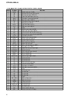
STR-KSL40/SL40
Pin No.
53
54
55
56
57
58
59
60
61
62
63
64 to 66
67 to 69
70
71
72 to 75
76
77 to 80
81
82 to 85
86
87
88
89
90
91
92 to 97
98,99
100
101
102 to 105
106
107,108
109,110
111
112
113
114
115
116
117 to 119
120
Pin Name
PAGE0
BOOT
BTACT
BST
MOD1
MOD0
EXLOCK
VDDI
VSS
A17
A16
A15 to A13
GP10 to GP8
VDDI
VSS
D15/GP7 to D12/GP4
VDDE
D11/GP3 to D8/GP8
VSS
A9 to A10
TDO
TMS
XTRST
TCK
TDI
VSS
A8 to A3
D7,D6
VDDI
VSS
D5 to D2
VDDE
D1,D0
A2,A1
VSS
A0
PM
SD13
SD14
SYNC
VSS
VDDI
I/O
O
I
O
I
I
I
I
—
—
O
O
O
I/O
—
—
I/O
—
I/O
—
O
O
I
I
I
I
—
O
I/O
—
—
I/O
—
I/O
O
—
O
I
I
I
I
—
—
Description
Not used (open)
Not used (connected to ground)
Not used (open)
Boot strap signal input from MB90478
Mode input (connected to VDD)
Mode input (connected to ground)
Lock signal input to LC89056W
Power supply (+2.5V)
Ground
Not used (open)
Not used (open)
Address bus output to the SRAM
External memory data I/O general purpose port terminal GP
Power supply (+2.5V)
Ground
SRAM data bus
Power supply (+3.3V)
SRAM data bus
Ground
Address bus output to the SRAM
Not used (open)
Not used (open)
Not used (open)
Not used (open)
Not used (open)
Ground
Address bus output to the SRAM
SRAM data bus
Power supply (+2.5V)
Ground
SRAM data bus
Power supply (+3.3V)
SRAM data bus
Address bus output to the SRAM
Ground
Address bus output to the SRAM
PLL initialization input from MB90478
Not used (open)
Not used (open)
Synchronization / asynchronous selection input (pull up)
Ground
Power supply (+2.5V)


