background image

– 22 –

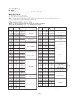
6. Power ON Procedure for Adjustment
(1)

Connect an extension cable to the adjusting remote commander.

(2)

After making sure that the HOLD switch on the adjusting remote commander is not turned on (not at left (NOR) position), supply 9.0
Vdc to the DC IN (J301).
(With the HOLD switch at HOLD position, the initial operation of the set does not finish, disabling the POWER switch function.)

(3)

Turn ON the POWER switch on the set. Confirm that a green LED lights up.

(4)

Set the HOLD switch on the adjusting remote commander to the HOLD (right (ADJ)) position.

7. Adjustment Finishing Procedure

Order

Page

Address

Data

Description

Remarks

1.

D

01 – 4B

Check if adjusted data are written correctly to the given page and address.

2.

2

00

00

Set 00 to given page and address.

Page 2: Reset

3.

1

00

00

Page D: Write protect

4.

Set HOLD switch on adj. remote commander to NOR position.

8. Password Reset (for operation check of the set)
(1)

Turn the POWER switch on, then press the “Password Reset” at the bottom of Power Box to reset the password set by the customer.

(2)

Operating the jog dial, select “No” on the Password Set screen to set “disuse of password”.
Or,

Order

Page

Address

Data

Description

Remarks

1.

1

00

01

Set 01 to given page and address.

Page D: Cancel protect

2.

D

04

FF

Set FF to given page and address and press PAUSE.

Set disuse of password

Final:

After all adjustments and operation check finished, turn the POWER switch on, press the "Password Reset" at the bottom of Power Box, and
turn the POWER switch off.

9. EXT. VIDEO AUDIO mode: Turn the POWER switch on, and press and operate the jog dial from the initial screen.

Or,

Order

Page

Address

Data

Description

Remarks

1.

2

00

01

Set 01 to given page and address.

2.

2

2B

00

Set 00 to given page and address.

10. Picture and tone quality standard setting: Press the Menu key and SEL/PUSH EXEC “RESET” with the jog dial.

Or,

Set data 01 to page:1, address:00 to cancel the protect on page D.

Order

Page

Address

Data

Description

Remarks

D

3C

00

Ope. – Brightness: Center

D

3E

00

Ope. – Contrast: Center

D

3F

00

Set data 00 to given page and address, and press PAUSE.

Ope. – Bass boost: OFF

D

40

00

Ope.– Surround: OFF

D

41

00

Ope. – VOL. limit: OFF

Volume (Display unit) – Maximum

Summary of Contents for PLM-A55E

Page 1: ...SERVICE MANUAL GLASSTRON AEP Model UK Model SPECIFICATIONS PLM A55E 9 928 101 31 ...

Page 2: ...hematic Diagram YM 11P Board 1 3 53 4 9 Schematic Diagram YM 11P Board 2 3 SW 312P Board 57 4 10 Schematic Diagram YM 11P Board 3 3 61 4 11 Schematic Diagram SA 52P Board 64 4 12 Printed Wiring Board SA 52P Board 67 4 13 Printed Wiring Board RG 46P Board 69 4 14 Schematic Diagram RG 46P Board 71 5 EXPLODED VIEWS 83 6 ELECTRICAL PARTS LIST 86 Notes on chip component replacement Never reuse a discon...

Page 3: ... 3 SECTION 1 GENERAL This section is extracted from instruction manual ...

Page 4: ... 4 ...

Page 5: ... 5 ...

Page 6: ... 6 ...

Page 7: ... 7 ...

Page 8: ... 8 ...

Page 9: ... 9 ...

Page 10: ... 10 ...

Page 11: ... 11 ...

Page 12: ... 12 ...

Page 13: ... 13 ...

Page 14: ... 14 ...

Page 15: ...n the numerical order given SECTION 2 DISASSEMBLY 1 screw M1 4 3 0 1 three screws M1 4 3 0 2 FP30 flexible board CN405 3 optics overall section 4 1 front panel 6 RG 46 board 5 flexible board CN402 2 connector CN401 3 screw M1 7 5 flexible board CN403 5 FP 29 flexible board CN406 ...

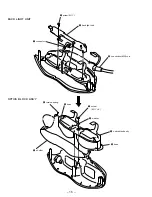
Page 16: ... 16 BACK LIGHT UNIT OPTICS BLOCK ASS Y 1 connector 2 screw M1 7 3 back light unit 4 connection MR cord 1 screw M1 7 4 2 washer 3 optics black ass y 4 boss 4 boss 6 torsion spring 5 shutter ...

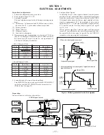
Page 17: ...me 6 B OUT 7 HP RET 8 R OUT 9 PCO 10 N C 6 Setting up Input Signals In adjusting this set video signals obtained from the pattern generator are used and therefore these video output signals must satisfy the specification Connect the oscilloscope to the VIDEO IN terminal and confirm that the sync signal amplitude of video signals is approximately 0 3 V the amplitude of video part is approximately 0...

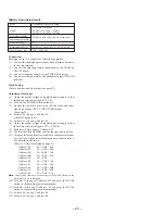
Page 18: ...0 V check Measurement point CL308 Specification value 1 85 0 10 V BL 7 0 V check Measurement point CL310 Specification value 7 00 1 00 V 3 Press the battery detection switch S705 on the SW 312P board Switch with fixed pawl at the lower right of battery Or short CN903 pin 1 and pin 2 on the YM 11P board CHARGE mode becomes active At this time confirm that the CHARGE LED orange lights up 4 Under thi...

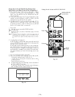
Page 19: ...ommander For the adjustment the adjustment data saved in the nonvolatile memory EEPROM must be rewritten and for this purpose the adjusting remote commander is used The adjusting remote commander makes two way communica tion with the product using a remote control signal line LANC The adjusting remote commander transmits pages addresses and data up down commands to the product The product trans mi...

Page 20: ...is pressed new data are not saved in the non volatile memory 4 Select page 1 address 00 and set 01 data Thus the data input to page D address 00 1A is enabled 5 After the adjustment finished select page 1 address 00 and set 00 data Thus the data change on page D is disabled 6 After all adjustments finished turn OFF the main power sup ply 9 0 V once 4 Precaution on Use of Adjusting Remote Commander...

Page 21: ... 7 8 9 A A B b C c D d E E F F 0 0 1 2 3 4 5 6 7 8 9 A A B b C c D d E E F F 1 2 3 4 5 6 7 8 9 10 11 12 13 14 15 16 17 18 19 20 21 22 23 24 25 26 27 28 29 30 31 32 33 34 35 36 37 38 39 40 41 42 43 44 45 46 47 48 49 50 51 52 53 54 55 56 57 58 59 60 61 62 63 64 65 66 67 68 69 70 71 72 73 74 75 76 77 78 79 80 81 82 83 84 85 86 87 88 89 90 91 92 93 94 95 96 97 98 99 100 101 102 103 104 105 106 107 108...

Page 22: ...er Box to reset the password set by the customer 2 Operating the jog dial select No on the Password Set screen to set disuse of password Or Order Page Address Data Description Remarks 1 1 00 01 Set 01 to given page and address Page D Cancel protect 2 D 04 FF Set FF to given page and address and press PAUSE Set disuse of password Final After all adjustments and operation check finished turn the POW...

Page 23: ...Address Data Remarks Initial set Memo 00 00 00 01 00 00 Fixed value 02 10 AEP UK 10 AEP UK 03 00 00 04 FF Set disuse of password 05 0A Set password 06 0A 07 Not used 08 09 0A Battery down adj 0B 0C 0D 10 10 Fixed value 0E 0F 10 Charge adjustment 11 12 13 56 56 14 F0 F0 15 14 14 16 28 28 17 0B 0B Fixed value 18 40 40 19 01 01 1A E0 E0 1B 01 01 1C 01 01 1D 1E 3F 3F Not used 1F 20 70 21 36 22 89 23 8...

Page 24: ...d audio signals are output EXT VIDEO AUDIO mode See page 22 4 Set data 01 to page 1 address 00 Cancel D page protect 5 Set data 01 to page 2 address 00 6 Adjust the output voltage of regulated power supply so that the battery terminal voltage is 5 77 0 02 Vdc 7 Read data ZZh on page 2 address 27 8 Confirm that the data ZZh satisfies the specification value 9 Using the following formulas calculatio...

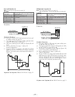
Page 25: ...C 6 Adjust the output voltage of regulated power supply so that the battery terminal voltage is 8 3 0 02 Vdc 7 Read data YYh on page 2 address 2D 8 Confirm that the data YYh satisfies the specification value 9 Using the following formulas calculation of hexadecimal numbers calculate the adjustment data and enter them to re spective adjustment addresses Refer to 5 Data Processing on page 21 Address...

Page 26: ... 11P board CN102 pin 6 Measuring equipment Oscilloscope Adjustment device RV101 on YM 11P board Specification value 2 2 0 1 µS VIDEO IN jack J101 Pattern Generator Set CN102 pin 0 SC OUT YM 11P Board Frequency Counter Oscilloscope DC range CN102 pin 6 HAFC CN102 pin 1 T GND YM 11P Board Connection Adjustment Procedure 1 Select EXT VIDEO AUDIO mode See page 22 2 Connect an oscilloscope to the CN102...

Page 27: ...e data so that the C level of waveform on the oscilloscope satisfies the specifi cation value Adjustment and Adjustment Parts RG 46P board see page 33 CN404 pin 9 PCO CN404 pin 1 GND RG 46P Board Oscilloscope DC range C 0 V Near center CN404 pin 4 G OUT CN404 pin 1 GND RG 46P Board Oscilloscope DC range 2H E RGB Brightness Adjustment Note The view angle correction must be turned off Condition Inpu...

Page 28: ... on the CH1 satisfies the specification value Adjustment and Adjustment Parts RG 46P board see page 33 Ch1 Ch2 CN404 pin 6 B OUT CN404 pin 1 GND RG 46P Board Oscilloscope DC range CN404 pin 4 G OUT CN404 pin 1 GND 2H E Oscilloscope DC range RG 46P Board CN404 pin 4 G OUT CN404 pin 1 GND D 2H Contrast Adjustment Note The view angle correction must be turned off Condition Input signal Chroma signal ...

Page 29: ...djustment Note The view angle correction must be turned off Before this adjustment the Contrast Adjustment must be finished Condition Input signal Chroma signal and color bar signal with burst signal turned off Measurement point RG 46P board CN404 pin 4 and pin 8 Measuring equipment Oscilloscope Adjustment page D Adjustment address 27 Specification value 0 05 V Connection Adjustment Procedure 1 Se...

Page 30: ...n the CH1 satisfies the specification value Adjustment and Adjustment Parts RG 46P board see page 33 Ch1 Ch2 CN404 pin 4 G OUT CN404 pin 1 GND RG 46P Board Oscilloscope DC range CN404 pin 8 R OUT CN404 pin 1 GND D 2H Burst Cleaning Adjustment When Anti pal signal is available perform the adjustment shown below When it isn t available fix the data Page D address 36 on A0h Note The view angle correc...

Page 31: ...IO mode and picture and tone qual ity standard setting See page 22 2 View angle correction ON Connect CN404 pin 2 EAC OFF and pin 1 GND on the RG 46P board 3 Set or confirm data 01 to page 1 address 00 Cancel D page protect 4 On page D address 29 change data with the PLAY and STOP buttons and press the PAUSE button to write data so that hori zontal streaks do not wobble on the display when looking...

Page 32: ...t EXT VIDEO AUDIO mode and picture and tone qual ity standard setting See page 22 2 View angle correction ON Connect CN404 pin 2 EAC OFF and pin 1 GND on the RG 46P board 3 Set or confirm data 01 to page 1 address 00 Cancel D page protect 4 Page D address 26 27 Change data at these two addresses with the PLAY and STOP buttons and press the PAUSE button to write data so that the display achromatic ...

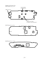
Page 33: ... CN102 CN902 IC902 IC901 RV101 OSD On Screen Display Horizontal sync frequency adjustment CN903 5 1 1 9 2 10 1 2 Connect adjusting remote commander VIDEO IN jack J101 YM 11P Board Conductor Side GND IC101 IC903 IC103 IC201 RG 46P Board Component Side CN404 IC401 1 9 2 10 ...

Page 34: ...en 18 TEST0 I 19 SLCK I Fixed at L in this set 20 VST2 O Vertical start pulse output to the left LCD unit Output of vertical scanning start pulse signal added to gate driver 21 VST1 O Vertical start pulse output to the right LCD unit Output of vertical scanning start pulse signal added to gate driver 22 VCK2 O 23 VCK1 O 24 EN O Enable pulse signal output to the left and right LCD units 25 CLR O Cl...

Page 35: ...T I Hue adjustment terminal also used for reset input Not used open 53 COLOR I Color adjustment terminal Not used open 54 XVXO I VXO crystal oscillator connection terminal 3 58 MHz Not used open 55 R BRT I R brightness adjustment signal input from the D A converter IC402 56 B BRT I B brightness adjustment signal input from the D A converter IC402 57 RGB GAIN I For adjusting the amplitude gain of R...

Page 36: ...king signal output for the cut video signals Not used open 13 SDE O Vertical sync detection signal output to the system controller IC903 L vertical sync signal present 14 VSYO O 15 HSYO O Horizontal sync signal output from the APC circuit Not used open 16 AVDD Power supply terminal 5V 17 VBSO O Output of composite video signal mixed with character signal 18 VCNT I For adjusting output level of com...

Page 37: ...the bypass selection Normally fixed at L 13 PLLSEL I For setting whether clock is entered by color subcarrier input built in PLL operation or by external clock input L built in PLL operation fixed at L in this set 14 ADGND Ground terminal for A D converter 15 ADVDD Power supply terminal 5V for A D converter 16 CLC I For setting time constant for internal clamp circuit Normally fixed at H 17 CLOUT ...

Page 38: ... at H in this set 15 SYNC O Composite sync signal output terminal L active Not used open 16 BF O Burst flag signal output terminal L active Not used open 17 YCLPTC Connected to the time constant circuit for pedestal clamp 18 ACKOUT O ACK auto color killer on off check signal output terminal L ACK on when APC is unlocked H normal when APC is locked Not used open 19 ALTOUT O Alternate pulse output i...

Page 39: ...nal output to the DC DC converter IC301 H power on 18 P13 E113 Not used open 19 BATT IN SW I Battery pack detection switch input terminal L battery pack present 20 P15 Not used open 21 POWER SW I Power switch S701 input terminal toggle input L is input when power is turned on off 22 P17 Not used open 23 SYSTEM RESET O Reset signal output to the character generator IC101 L reset 24 POWER LED O LED ...

Page 40: ...elect signal output to the character generator IC101 79 DD MAIN O Main power supply control signal output to the DC DC converter IC301 80 SHUTTER O Rectangle waveform 125 Hz output for the shutter Not used open 81 AVSS Ground terminal for A D input 82 MENU EXEC A D I S702 and S703 keys input on the SA 52P board 83 BATT SIG I Not used 84 CHARGE A D IN I Input of battery voltage detection in charge ...

Page 41: ...2 BB1 SURROUND AU MUTE DIAL 2 DIAL 1 MENU EXEC AU EVR HP R HP L HP RET HP R HP L HP RET SCK HP RCS EVR EVR DO LANC DC LANC SIG LANC SIG POWER SW MENU EXEC A D DIAL A PHASE DIAL B PHASE AUDIO MUTE SURROUND BB1 ON BB2 ON AVLS ON POWER SW LANC OUT LANC IN X1 X0 CL0 CL1 14 15 13 7 VSYO OSC COIL L P F L P F BUFFER Q602 BUFFER Q601 FILTER ADC VCO DAC DAC CONTROL LOGIC CONTROL LOGIC CLOCK GENERATOR APCG ...

Page 42: ... 16 AU MUTE 1 1 2 2 4 3 6 SURROUND AMP IC503 1 3 SURROUND AMP IC503 1 3 SURROUND SWITCH IC502 8 9 10 14 13 12 AMP Q502 AMP IC503 1 3 5 AU L AU R DC BIAS IC501 8 14 15 10 DIAL 1 DIAL 2 POWER SW 13 12 POWER LED CHARGE LED S702 POWER MENU 2 21 3 3 6 7 MENU EXEC AU EVR 7 ON OFF CHARGE D701 D702 S701 ELECTRICAL VOLUME 1 2 8 5 AMP Q501 TO MAIN BLOCK CN701 TO MAIN BLOCK PUSH DISPLAY SEL PUSH EXEC S703 1 ...

Page 43: ...9 SWITCHING REGULATOR Q312 SWITCHING REGULATOR Q310 RE B OUT SCP B RE D OUT SCP D RE C OUT SCP C VCC CTL C D POWER CONT SWITCHING REGULATOR Q313 RE B OUT SCP B B IN DC DC CONVERTER IC301 2 2 BATT 8 4V BL 7V CHARGE A D IN DD CHARGE BATT CHK DD MAIN DD POWER BATT IN BATT SENSE DC IN MON BATT CONT BATT IN SW DC IN A D BATT IN MON SYSTEM CONTROLLER IC903 B SWITCH Q305 306 A D SWITCH Q307 RESET SIGNAL ...

Page 44: ...ces Waveforms are taken with a oscilloscope Voltage variations may be noted due to normal produc tion tolerances Circled numbers refer to waveforms Signal path g VIDEO Y CHROMA L VIDEO Y F VIDEO CHROMA N VIDEO color difference signal N VIDEO R G B J AUDIO Note The components identified by mark or dotted line with mark are critical for safety Replace only with part number specified 49 C B These are...

Page 45: ... 53 54 55 56 4 8 SCHEMATIC DIAGRAM YM 11P Board 1 3 See pages 80 and 81 for Waveforms See pages 75 to 78 for IC Block Diagrams PLM A55E Page 60 Page 57 Page 60 Page 63 Page 71 Page 63 ...

Page 46: ...60 4 9 SCHEMATIC DIAGRAM YM 11P Board 2 3 SW 312P Board See page 81 for Waveforms See pages 75 to 78 for IC Block Diagrams PLM A55E Page 57 Page 66 Page 71 Page 63 Page 63 Page 61 Page 63 Page 61 Page 53 Page 53 ...

Page 47: ...PLM A55E 61 62 63 4 10 SCHEMATIC DIAGRAM YM 11P Board 3 3 See pages 81 and 82 for Waveforms See pages 75 to 78 for IC Block Diagrams Page 57 Page 57 Page 57 Page 57 Page 56 Page 57 Page 53 ...

Page 48: ... 64 65 66 4 11 SCHEMATIC DIAGRAM SA 52P Board See page 75 for IC Block Diagrams PLM A55E Page 57 ...

Page 49: ... Semiconductor Location Conductor Side Ref No Location D507 C 3 D701 B 2 D702 A 2 D703 B 2 D704 C 2 D708 C 2 Q511 D 3 D501 D 2 D502 D 2 D505 D 3 D509 C 3 D510 C 3 D511 C 3 D705 B 1 D706 A 2 D707 A 1 D709 A 2 IC501 C 2 IC502 C 1 IC503 D 1 IC504 D 2 Q501 C 2 Q502 B 2 Q503 D 2 Q508 D 3 Q512 C 3 Q701 A 2 Page 51 ...

Page 50: ...nductor Location Component Side Ref No Location D406 A 7 IC402 A 3 Q401 B 5 Q402 A 4 Q405 A 7 Q406 A 4 Q407 B 4 Q408 A 5 Q409 A 5 D405 A 7 D407 B 6 IC401 A 6 Q403 A 7 Q404 A 7 Q410 A 2 Q411 A 1 Semiconductor Location Conductor Side Ref No Location Page 52 Page 52 ...

Page 51: ... 71 72 73 74 PLM A55E 4 14 SCHEMATIC DIAGRAM RG 46P Board See page 82 for waveforms See pages 77 to 79 for IC Block Diagrams Page 56 Page 57 ...

Page 52: ...20 19 18 23 24 22 21 17 4 3 5 8 7 6 A D CONVERTER D A CONVERTER CONTROL LOGIC APCF I PROCESSING MODE CONTROL LOGIC 2H 1H BIAS CONTROL LOGIC CLOCK GENERATOR CLAMP RTP VCOVDD BIAS OSCV DAGND YOUT DAVDD COUT DAREF OUTSW VREG VCLPTC ALTOUT ACKOUT SYNCTC YCLPTC DLABIAS ACKTC COUT G Y R Y G Y B Y DLAIN R R Y ACCTC VCC1 GND1 SHPCTL SHPF0 TPADJ CADJ BF SYNC 2 1 13 11 10 9 12 14 15 16 28 30 31 CIN 32 29 27...

Page 53: ...51 52 53 54 56 57 58 60 62 63 64 61 55 59 PAL PULSE ELIM MODE SEL FIELD LINE CTL POL SW SUB BRIGHT RGB GAIN GAMMA BRIGHT S H SUB CONTRAST LPF MATRIX CONTRAST EXT SW DEMOD INT EXT CLAMP PAL ID PAL SW RESET APC VXO HUE PS ACC DET KILLER COLOR CONT FILT CAL REG REGV 5V 12V VCC 2 1 2 R Y IN C OUT HUE RST XVXO R BRT B BRT RGB GAIN GAMMA 2 GAMMA 1 COLOP BRIGHT CONTRAST C IN R GAIN PIC CONT AGC DL 2 DL 1...

Page 54: ...3 ª CLK IN 8 IC103 5 Y OUT 9 IC103 7 C OUT 0 Q257 Emitter Q254 Emitter Q264 Emitter IC201 VIDEO IN IC201 CIN IC201 4 VX01 4 9 Vp p H 0 5 Vp p H 0 5 Vp p H H 5 0 Vp p 3 Vp p 17 734475 MHz 0 7 Vp p H 1 0 Vp p 279 ns 380 mVp p H H 270 mVp p 400 mVp p H 440 mVp p H 536 mVp p H 136 mVp p H H 144 mVp p 980 mVp p 4 433619 MHz ...

Page 55: ... B Y IC201 0 R R Y YM 11P Board 3 3 1 IC301 CT 2 IC301 1 CA1 3 IC301 CA2 4 IC301 NF A 5 IC301 NF C 560 mVp p 4 433619 MHz 1 6 Vp p H 1 2 Vp p H 5 0 Vp p 10 MHz 1 6 Vp p 32 KHz 640 mVp p 3 36 µs 3 7 Vp p 3 27 µs 2 4 Vp p 3 27 µs 2 5 Vp p 3 27 µs 2 5 Vp p 3 27 µs 880 mVp p 3 27 µs 16 8 Vp p 3 27 µs 1 5 Vp p 3 27 µs ...

Page 56: ...7 IC401 ª R OUT 8 IC401 G OUT 9 IC401 B OUT 0 IC401 ª B Y IN IC401 º R Y IN SA 52P Board 1 Q407 Base 2 Q402 Base 960 mVp p 3 27 µs 1 2 Vp p 3 27 µs 540 mVp p H 392 mVp p H 424 mVp p H 300 mVp p H 1 4 Vp p 60 6 ns 4 8 Vp p 2 V 9 6 Vp p H 9 6 Vp p H 9 6 Vp p H 224 mVp p H 204 mVp p H ...

Page 57: ...lor Ref No Part No Description Remark Ref No Part No Description Remark 1 3 988 749 03 PANEL FRONT 2 3 988 805 02 SHUTTER 3 3 988 747 12 CABINET LOWER 4 X 3948 502 3 PLATE ASSY CLICK 5 3 973 497 31 SCREW M1 7 0 NO P 2 6 A 8044 826 A OPTICS COMPLETE ASSY 7 3 988 761 01 SPRING TORSION 8 3 050 316 01 WASHER 9 3 713 791 71 SCREW M1 7X4 10 1 475 821 11 LIGHT UNIT BACK 11 A 8054 837 A RG 46P BOARD COMPL...

Page 58: ...T R ASSY 68 3 988 782 01 BUTTON R RELEASE 69 X 3948 705 1 PLATE R ASSY SLIDE 70 3 989 031 01 HOOK R REAR BELT 71 A 7093 797 A BELT BLOCK ASSY HEAD 72 A 7083 699 A PAD BLOCK ASSY 73 3 050 317 01 PAD 74 3 989 032 01 HOOK L REAR BELT 75 3 988 783 01 BUTTON L RELEASE 76 X 3948 706 1 PLATE L ASSY SLIDE 77 3 988 775 02 CABINET L REAR HORIZONTAL 78 3 050 033 01 SPRING L HP LOCK 79 X 3948 505 2 CABINET L ...

Page 59: ...D COMPLETE 105 3 945 884 11 SCREW 2X6 106 1 777 761 11 WIRE FLAT TYPE 24 CORE 107 1 694 076 21 TERMINAL BOARD BATTERY 108 3 988 800 01 RETAINER TERMINAL 109 A 8054 836 A SW 312P BOARD COMPLETE 110 A 8054 833 A YM 11P BOARD COMPLETE 111 1 783 687 12 CORD CONNECTION MR 112 X 3948 507 1 CABINET IF ASSY LOWER 113 3 740 607 01 CUSHION 114 1 958 979 11 HARNESS SY 101 102 103 106 104 105 105 108 107 109 ...

Page 60: ...1uF 25V C423 1 107 682 91 CERAMIC CHIP 1uF 10 16V C424 1 117 920 91 TANTAL CHIP 10uF 20 6 3V C425 1 164 156 91 CERAMIC CHIP 0 1uF 25V C426 1 164 156 91 CERAMIC CHIP 0 1uF 25V C427 1 109 982 91 CERAMIC CHIP 1uF 10 10V C428 1 113 994 91 TANTAL CHIP 6 8uF 20 16V C429 1 164 156 91 CERAMIC CHIP 0 1uF 25V C430 1 117 396 91 TANTAL CHIP 3 3uF 20 10V C431 1 164 156 91 CERAMIC CHIP 0 1uF 25V C432 1 117 396 ...

Page 61: ...S CHIP 680 5 1 16W R422 1 216 833 91 RES CHIP 10K 5 1 16W R423 1 216 833 91 RES CHIP 10K 5 1 16W R424 1 216 833 91 RES CHIP 10K 5 1 16W R425 1 216 837 91 RES CHIP 22K 5 1 16W R426 1 216 839 91 RES CHIP 33K 5 1 16W R427 1 216 815 91 RES CHIP 330 5 1 16W R428 1 216 833 91 RES CHIP 10K 5 1 16W R429 1 216 833 91 RES CHIP 10K 5 1 16W R430 1 216 821 91 RES CHIP 1K 5 1 16W R431 1 216 833 91 RES CHIP 10K ...

Page 62: ...AMIC CHIP 22PF 5 50V C512 1 126 198 21 ELECT CHIP 4 7uF 20 35V C513 1 126 198 21 ELECT CHIP 4 7uF 20 35V C516 1 124 778 21 ELECT CHIP 22uF 20 6 3V C519 1 164 156 91 CERAMIC CHIP 0 1uF 25V C522 1 164 156 91 CERAMIC CHIP 0 1uF 25V C524 1 164 156 91 CERAMIC CHIP 0 1uF 25V C525 1 124 778 21 ELECT CHIP 22uF 20 6 3V C526 1 164 346 91 CERAMIC CHIP 1uF 16V C527 1 124 779 21 ELECT CHIP 10uF 20 16V C528 1 1...

Page 63: ... 2 5 1 16W R554 1 216 789 91 RES CHIP 2 2 5 1 16W R556 1 216 798 91 RES CHIP 12 5 1 16W R557 1 216 798 91 RES CHIP 12 5 1 16W R560 1 216 864 91 SHORT 0 R562 1 216 863 91 RES CHIP 3 3M 5 1 16W R565 1 216 864 91 SHORT 0 R566 1 216 821 91 RES CHIP 1K 5 1 16W R567 1 216 821 91 RES CHIP 1K 5 1 16W R701 1 216 825 91 RES CHIP 2 2K 5 1 16W R702 1 216 864 91 SHORT 0 R703 1 216 817 91 RES CHIP 470 5 1 16W R...

Page 64: ...2 1 164 156 91 CERAMIC CHIP 0 1uF 25V C243 1 164 156 91 CERAMIC CHIP 0 1uF 25V C244 1 164 156 91 CERAMIC CHIP 0 1uF 25V C251 1 162 964 91 CERAMIC CHIP 0 001uF 10 50V C253 1 135 259 91 TANTAL CHIP 10uF 20 6 3V C255 1 162 974 91 CERAMIC CHIP 0 01uF 50V C257 1 135 259 91 TANTAL CHIP 10uF 20 6 3V C263 1 164 156 91 CERAMIC CHIP 0 1uF 25V C264 1 135 259 91 TANTAL CHIP 10uF 20 6 3V C265 1 135 259 91 TANT...

Page 65: ...3V C953 1 164 156 91 CERAMIC CHIP 0 1uF 25V C954 1 162 974 91 CERAMIC CHIP 0 01uF 50V C955 1 164 156 91 CERAMIC CHIP 0 1uF 25V CONNECTOR CN101 1 770 624 21 PIN CONNECTOR 7P CN102 1 573 984 21 CONNECTOR BOARD TO BOARD 10P CN103 1 770 626 21 PIN CONNECTOR 9P CN301 1 573 768 21 PIN CONNECTOR 1 5mm SMD 5P CN901 1 779 336 21 CONNECTOR FFC FPC 24P CN902 1 691 550 21 PIN CONNECTOR 1 5mm SMD 3P CN903 1 69...

Page 66: ...TX Q130 8 729 420 29 TRANSISTOR 2SD1819A QRS TX Q131 8 729 420 29 TRANSISTOR 2SD1819A QRS TX Q134 8 729 420 29 TRANSISTOR 2SD1819A QRS TX Q135 8 729 420 29 TRANSISTOR 2SD1819A QRS TX Q150 8 729 420 26 TRANSISTOR 2SB1218A QRS TX Q151 8 729 420 26 TRANSISTOR 2SB1218A QRS TX Q152 8 729 420 29 TRANSISTOR 2SD1819A QRS TX Q153 8 729 420 26 TRANSISTOR 2SB1218A QRS TX Q154 8 729 420 29 TRANSISTOR 2SD1819A...

Page 67: ... R154 1 216 826 91 RES CHIP 2 7K 5 1 16W R155 1 216 821 91 RES CHIP 1K 5 1 16W R157 1 216 825 91 RES CHIP 2 2K 5 1 16W R158 1 216 805 91 RES CHIP 47 5 1 16W R159 1 216 823 91 RES CHIP 1 5K 5 1 16W R160 1 216 864 91 SHORT 0 R162 1 216 864 91 SHORT 0 R164 1 216 833 91 RES CHIP 10K 5 1 16W R166 1 216 833 91 RES CHIP 10K 5 1 16W R168 1 216 833 91 RES CHIP 10K 5 1 16W R169 1 216 833 91 RES CHIP 10K 5 1...

Page 68: ... 1 216 833 91 RES CHIP 10K 5 1 16W R297 1 216 833 91 RES CHIP 10K 5 1 16W R298 1 216 833 91 RES CHIP 10K 5 1 16W R299 1 543 949 22 FERRITE 0uH R301 1 218 887 91 RES CHIP 47K 0 50 1 16W R302 1 218 887 91 RES CHIP 47K 0 50 1 16W R303 1 216 833 91 RES CHIP 10K 5 1 16W R304 1 218 867 91 RES CHIP 6 8K 0 50 1 16W R305 1 218 859 91 RES CHIP 3 3K 0 50 1 16W R306 1 216 206 91 RES CHIP 2 2K 5 1 8W R307 1 21...

Page 69: ...16W R922 1 216 833 91 RES CHIP 10K 5 1 16W R923 1 216 821 91 RES CHIP 1K 5 1 16W R924 1 216 851 91 RES CHIP 330K 5 1 16W R925 1 216 853 91 RES CHIP 470K 5 1 16W R926 1 216 849 91 RES CHIP 220K 5 1 16W R927 1 216 833 91 RES CHIP 10K 5 1 16W R928 1 216 817 91 RES CHIP 470 5 1 16W R929 1 216 864 91 SHORT 0 R930 1 216 864 91 SHORT 0 R932 1 216 864 91 SHORT 0 R933 1 216 821 91 RES CHIP 1K 5 1 16W R934 ...

Page 70: ...PT 2 SET R RV401 1 225 661 11 RES VAR CARBON 50K VOL ACCESSORIES PACKING MATERIALS 1 475 456 22 ADAPTOR AC AC PLM2 1 590 866 41 CORD POWER UK 1 575 131 31 CORD POWER AEP 1 777 690 11 CORD CONNECTION 1 783 829 11 CABLE AV MONITOR 3 862 932 31 MANUAL INSTRUCTION ENGLISH FRENCH AEP 3 862 932 41 MANUAL INSTRUCTION GERMAN DUTCH AEP 3 862 932 51 MANUAL INSTRUCTION SWEDISH FINNISH AEP 3 862 932 61 MANUAL...

Reviews: