MZ-R701/R701DPC
34
34
1
A
B
C
D
E
F
G
H
I
J
2
3
4
5
6
7
8
9
10
11
12
13
14
OPTICAL
PICK-UP
BLOCK
(LCX-4R)
R1036
R1046
R1024
L906
L602
R609
Q603
R840
D803
D607
R611
R610
C628
R839
R834
C801
C825
C606
R603
C605
C604
C603
C612
C632
C611
C624
C615
R814
F801
C316
R105
J302 (1/2)
J301 (1/2)
LINE IN
(OPTICAL)
T601
TP606
TP317
TP315
TP314
TP901(VC)
TP912
(GND)
TP313
TP312
TP311
TP345
TP344
TP341
TP343
TP336
TP338
TP337
TP333
(D-IN)
TP332
(DGND)
TP331
(DVCC)
AP555
AP557
AP550
AP566
AP553
AP551
TP1003
AP556
AP558
AP502
AP560
AP587
AP583
AP563
AP501
AP568
TP339
MAIN BOARD
(SIDE A)
TP335
TP1002
TP605
S805
(HALF LOCK)
TP604
TP1004
TP1001
AP586
TP801
TP334
TP342
TP518
TP902(VL)
TP505
TP519
TP501
TP512
TP316
TP306
TP307
L905
C518
C909
C910
C912
C913
R941
R920
R947
C524
L501
R907
R908
R921
R914
D904
C902
R909
R917
AP906
R910
C556
C529
C553
C554
RB553
C512
C557
C558
C559
C561
C555
L904
C904
R521
R519
Q501
L502
CN501
C522
L301
L552
L801
C822
C830
C818
R807
C810
C811
C827
C823
L802
C804
R836
L551
C104
C204
L902
L901
L601
C630
FB804
FB802
R1040
R1025
1
1 3 5 7
2 4 6 8
5
8
4
1
D603
R607
R619
R602
C926
C919
R601
D601
Q601
C920
R915
C602
56
50
45 43
5
10
15
20
25
28
29
35
40
42
IC551
IC804
B C E
AP830
TP603
AP907
AP831
1
4
8
5
1
5
10
15
20
R815
R831
C521
R830
GD
S
(RVCC)
(DTCK)
(KEY-R)
(RGND)
11
(11)
S806
(OPEN/CLOSE DETECT)
TP(+)
TP(–)
1-679-264-
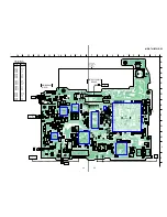
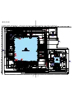
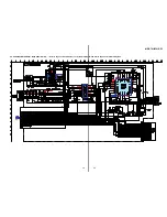
6-5. PRINTED WIRING BOARD — MAIN SECTION —
Note:
•
Y
: parts extracted from the conductor side.
•
: Pattern from the side which enables seeing.
(The other layer’s patterns are not indicated.)
surface
Lead layout of conventional IC
CSP (chip size package)
Caution:
Pattern face side: Parts on the pattern face side seen from the
(Side B)
pattern face are indicated.
Parts face side:
Parts on the parts face side seen from the
(Side A)
parts face are indicated.
• Main board is four-layer printed board.
However, the patterns of layers 2 and 3 have not been in-
cluded in this diagrams.
*
Replacement of IC801 on
main board
requires a special tool.
•
Lead Layouts
D601
I-8
D603
I-6
D607
J-4
D803
G-4
D904
I-7
IC551
D-6
IC804
E-4
Q501
F-8
Q601
J-7
Q603
I-3
• Semiconductor
Location (SIDE A)
Ref. No.
Location


