
3
MV-65ST
TABLE OF CONTENTS
1.
SERVICING NOTES
...............................................
3
2.
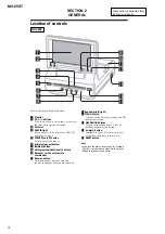
GENERAL
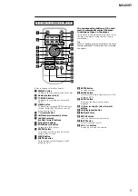
Location of Controls .......................................................
4
3.
DISASSEMBLY
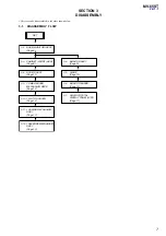
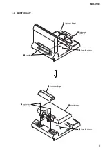
3-1. Disassembly Flow ...........................................................
7
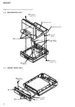
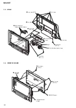
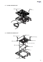
3-2. Base (Monitor) Assy .......................................................
8
3-3. Cabinet (Front) Assy .......................................................
8
3-4. Monitor Assy ...................................................................
9
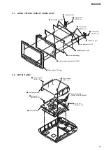
3-5. Hinge ............................................................................... 10
3-6. MONITOR Board ........................................................... 10
3-7. Liquid Crystal Display Panel (LCD1) ............................ 11
3-8. DVD MD Assy ................................................................ 11
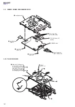
3-9. COMBO Board, Mechanism Deck ................................. 12
3-10. TD-S-Top-Cover ............................................................. 12
3-11. Loading Mechanism Assy ............................................... 13
3-12. Traverse Mechanism Assy .............................................. 13
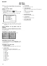
4.
TEST MODE
.............................................................. 14
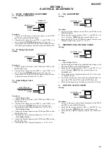
5.
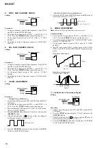
ELECTRICAL ADJUSTMENTS
......................... 15
6.
DIAGRAMS
6-1. Block Diagram – AUDIO Section – ............................... 18
6-2. Block Diagram – VIDEO, PANEL Section – ................ 19
6-3. Block Diagram – POWER Section – .............................. 20
6-4. Note for Printed Wiring Boards
and Schematic Diagrams ................................................ 21
6-5. Printed Wiring Board
– MONITOR Board (Side A) – ...................................... 22
6-6. Printed Wiring Board
– MONITOR Board (Side B) – ...................................... 23
6-7. Schematic Diagram – MONITOR Board (1/4) – ........... 24
6-8. Schematic Diagram – MONITOR Board (2/4) – ........... 25
6-9. Schematic Diagram – MONITOR Board (3/4) – ........... 26
6-10. Schematic Diagram – MONITOR Board (4/4) – ........... 27
6-11. Printed Wiring Board – KEY Board – ............................ 28
6-12. Schematic Diagram – KEY Board – .............................. 29
6-13. Schematic Diagram – POWER Section (1/2) – .............. 30
6-14. Schematic Diagram – POWER Section (2/2) – .............. 31
6-15. Printed Wiring Board – POWER Board (Side A) – ....... 32
6-16. Printed Wiring Board – POWER Board (Side B) – ....... 33
6-17. Printed Wiring Board – AMP Section – ......................... 34
7.
EXPLODED VIEWS
7-1. Overall Section ................................................................ 46
7-2. Cabinet (Front) Section ................................................... 47
7-3. Base (Monitor) Section ................................................... 48
7-4. Monitor Section ............................................................... 49
7-5. Cabinet (Lower) Section-1 .............................................. 50
7-6. Cabinet (Lower) Section-2 .............................................. 51
7-7. Mechanism Deck Section-1 ............................................ 52
7-8. Mechanism Deck Section-2 ............................................ 53
7-9. Mechanism Deck Section-3 ............................................ 54
8.
ELECTRICAL PARTS LIST
............................ 55
NOTES ON HANDLING THE OPTICAL PICK-UP
BLOCK OR BASE UNIT
The laser diode in the optical pick-up block may suffer electro-
static break-down because of the potential difference generated
by the charged electrostatic load, etc. on clothing and the human
body.
During repair, pay attention to electrostatic break-down and also
use the procedure in the printed matter which is included in the
repair parts.
The flexible board is easily damaged and should be handled with
care.
NOTES ON LASER DIODE EMISSION CHECK
Never look into the laser diode emission from right above when
checking it for adjustment. It is feared that you will lose your sight.
UNLEADED SOLDER
Boards requiring use of unleaded solder are printed with the lead-
free mark (LF) indicating the solder contains no lead.
(Caution: Some printed circuit boards may not come printed with
the lead free mark due to their particular size)
: LEAD FREE MARK
Unleaded solder has the following characteristics.
•
Unleaded solder melts at a temperature about 40
°
C higher than
ordinary solder.
Ordinary soldering irons can be used but the iron tip has to be
applied to the solder joint for a slightly longer time.
Soldering irons using a temperature regulator should be set to
about 350
°
C.
Caution: The printed pattern (copper foil) may peel away if the
heated tip is applied for too long, so be careful!
•
Strong viscosity
Unleaded solder is more viscou-s (sticky, less prone to flow)
than ordinary solder so use caution not to let solder bridges oc-
cur such as on IC pins, etc.
•
Usable with ordinary solder
It is best to use only unleaded solder but unleaded solder may
also be added to ordinary solder.
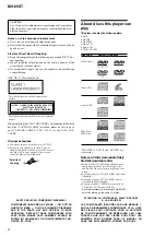
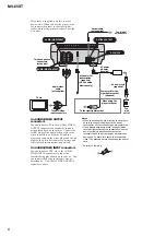
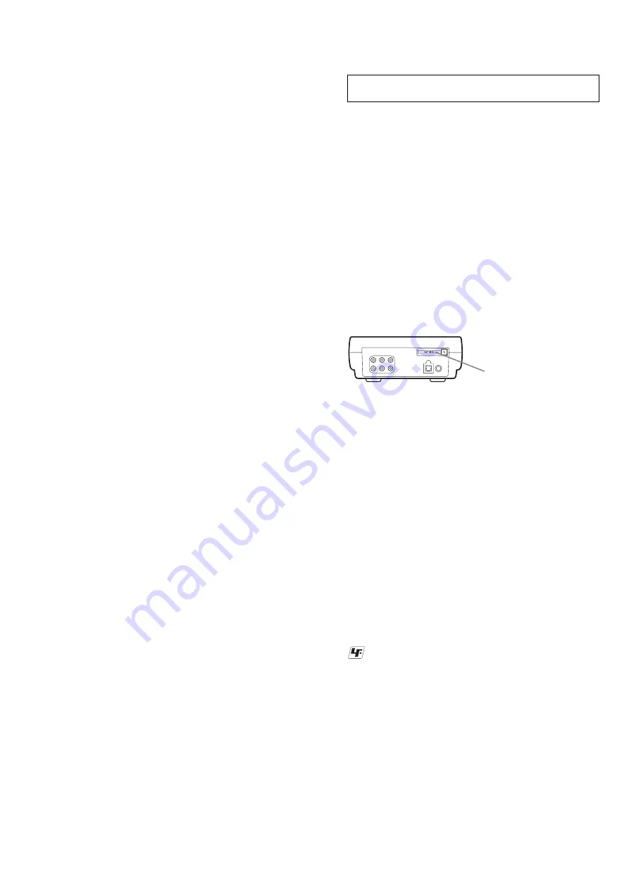
For E model NTSC type and PAL type.
The type of an NTSC system and the type of a PAL system exist in
E model.
Please refer to the following figure about how to recognize.
NTSC: NTSC TYPE
PAL: PAL TYPE
– BACK VIEW –
SECTION 1
SERVICING NOTES