background image

3

SECTION  1

GENERAL

This section is extracted from
instruction manual.

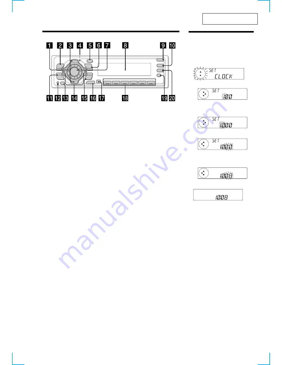
Location of controls

Refer to the pages listed for details.

1

Volume control dial  19

2

MENU button  8, 10, 12, 13, 14, 15, 16,
18, 19, 21, 24

3

DISC/PRST +/– (cursor up/down) buttons
8, 10, 12, 13, 14, 15, 16, 18, 19, 20, 21, 24

During CD/MD playback:

Disc change  10, 13

During radio reception:

Preset stations select  16

4

Z

 (eject) button (located on the front

side of the unit behind the front panel)
9

5

DSPL/PTY (display mode change/
programme type) button  9, 10, 12, 17,
20

6

LIST button  12

List-up

  13

7

SOURCE (TUNER/CD/MD) button
8, 9, 10, 13, 15, 16, 19

8

Display window

9

OPEN button  7, 9, 26

q;

D-BASS button  25

qa

SOUND button  23

qs

Reset button (located on the front side
of the unit behind the front panel)  7

qd

OFF button

*

  7, 8, 9

qf

SEEK/AMS –/+ (cursor left/right) buttons
8, 10, 12, 14, 16, 18, 19, 21, 23, 24

Automatic Music Sensor 

 10, 14

Manual Search 

 10

Seek  

15, 16, 18

qg

ENTER button  8, 10, 12, 13, 14, 15, 16,
18, 19, 20, 21, 24

qh

MODE button  19
During CD or MD playback:

CD/MD unit select  9, 13

During radio reception:

BAND select  15, 16

qj

Receptor for the card remote
commander

qk

Number buttons
During radio reception:

Preset number select  15, 16, 18, 19

During CD/MD playback:

(1)

REP  11

(2)

SHUF  11

ql

AF button  17, 18, 19

w;

TA button  18, 19

*

Warning when installing in a car
without ACC (accessory) position on
the ignition key switch

Be sure to press 

(OFF)

 on the unit for two

seconds to turn off the clock display after
turning off the engine.

When you press 

(OFF)

 only momentarily,

the clock display does not turn off and this

causes battery wear.

MDX-C6500RX/C6500R
/C6400R

D I SC

+

PR

S

T

+

-

D IS C

PR

ST

- -

LIST

DSPL

AF

OFF

PTY

ENTER

MENU

SOUND

1

2

3

4

5

6

SOURCE

-SEEK/AMS

REP

SHUF

TA

OPEN

D-BASS

MODE

Setting the clock

The clock uses a 24-hour digital indication.

Example: To set the clock to 10:08

1

Press 

(MENU)

, then press either side of

(DISC/PRST)

 repeatedly until “CLOCK”

appears.

1

Press 

(ENTER)

.

The hour indication flashes.

2

Press either side of 

(DISC/PRST)

 to set

the hour.

3

Press the (+) side of 

(SEEK/AMS)

.

The minute indication flashes.

4

Press either side of 

(DISC/PRST)

 to set

the minute.

2

  Press 

(ENTER)

.

The clock starts.

After the clock setting is completed, the
display returns to normal play mode.

Tip
You can set the clock automatically with the RDS
feature (see page 17).

Note
In the initial setting, the clock indication appears
while the unit is turned off.
When the D.INFO mode is set to ON, the time is
always displayed (page 24).

Summary of Contents for MDX-C6400R

Page 1: ...ediate frequency 10 7 MHz 450 kHz Sensitivity MW 30 µV LW 40 µV Power amplifier section Outputs Speaker outputs sure seal connectors Speaker impedance 4 8 ohms Maximum power output 50 W 4 at 4 ohms General Outputs Audio outputs 1 Power aerial relay control lead Power amplifier control lead Telephone ATT control lead 2 Tone controls Bass 9 dB at 100 Hz Treble 9 dB at 10 kHz Power requirements 12 V ...

Page 2: ...r diode emission from right avove when checking it for adustment It is feared that you will lose your sight NOTES ON HANDLING THE OPTICAL PICK UP BLOCK KMS 241C J1NP The laser diode in the optical pick up block may suffer electro static break down easily When handling it perform soldering bridge to the laser tap on the flexible board Also perform m easures against electrostatic break down sufficie...

Page 3: ...ons During radio reception Preset number select 15 16 18 19 During CD MD playback 1 REP 11 2 SHUF 11 ql AF button 17 18 19 w TA button 18 19 Warning when installing in a car without ACC accessory position on the ignition key switch Be sure to press OFF on the unit for two seconds to turn off the clock display after turning off the engine When you press OFF only momentarily the clock display does n...

Page 4: ...4 ...

Page 5: ...5 ...

Page 6: ...6 ...

Page 7: ...7 ...

Page 8: ...8 ...

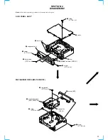
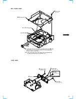
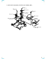
Page 9: ...er given MECHANISM DECK MG 164NZ 138 1 screw PTT2 6 5 2 cover 4 claw 3 screw PTT2 6 8 3 two screws PTT2 6 8 3 screw PTT2 6 8 5 sub panel ass y 4 two claws 6 flexible flat cable CNP811 1 screw PTT2 6 5 5 mechanism deck MG 164NZ 138 3 two screws PTT2 6 5 4 bracket MD 2 connector CN101 1 screw PTT2 6 5 ...

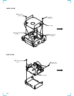
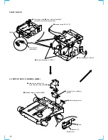
Page 10: ...10 SERVO BOARD MAIN BOARD 2 two screws BVTT2 4 1 sensor flexible board CN102 2 two screws BVTT2 4 1 flexible board CN103 3 servo board 1 three ground point screws 2 three screws PTT2 6 10 3 main board ...

Page 11: ...river etc disengage the Shaft MD Cover Guide from the slot in the MD Cover Assy Note Take care not to scratch the optiocal Pick up when pushing the Cassette Holder with a screwdriver etc shaft MD cover guide cassette holder A 1 three screws PTT2 6 10 2 two screws PTT2 6 12 1 screw PTT2 6 10 C6500R C6500RX 1 two screws PTT2 6 10 3 heat sink ...

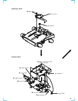
Page 12: ...rings FLOAT F 3 Pushing an arrow A part raise the float block up ward at the front to release a lock A float block lever lock R lever lock L 4 Remove the bracket LO in the direction of the arrow A bracket LO 1 Remove solders of motor M903 5 LO motor ass y loading M903 2 tension spring rack 3 claw A bottom view ...

Page 13: ...washer 2 lever LE ass y 3 roller GEAR E 1 2 type E stopring 1 5 2 type E stopring 1 5 3 lever lock L 2 type E stopring 1 5 2 type E stopring 1 5 4 Remove the holder ass y in the direction of the arrow 1 spring CHKG 1 spring CHKG 3 lever lock R ...

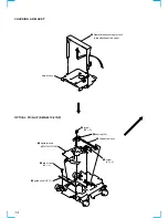
Page 14: ...C J1NP CHUCKING ARM ASS Y 1 Remove the chucking arm ass y in the direction of the arrow holder ass y 6 bearing SL 5 feed screw ass y 3 screw K2 3 2 guide shaft OPT L 1 two screws K2 3 7 optical pick up KMS 241C J1NP 4 screw B2 3 ...

Page 15: ...OR ASS Y SPINDLE M901 4 screw P1 7 1 8 5 bracket SL 9 two screws P1 7 1 8 0 bracket SP qa SP motor ass y spindle M901 7 screw B2 3 2 two screws 2 8 3 sensor board 1 Remove solders of motors M901 M902 8 base SL 6 SL motor ass y sled M902 ...

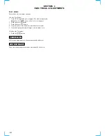
Page 16: ... if the clock is not displayed 2 Push the preset 4 button 3 Push the preset 5 button 4 Press the preset 1 button for more than two seconds 5 Then the display indicates all lights the test mode is set Release the Test mode 1 Push the OFF button MD SECTION MD section adjustments are done automatically in this set TUNER SECTION Tuner section adjustments are done automatically in this set ...

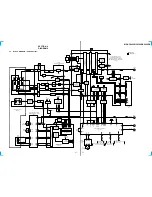
Page 17: ...ENCODER DECODER PLL FILTER 59 58 61 60 FILI PCO CLTV FILO 100 EFMO 23 ADDT IC301 1 2 15 TX COMPA RATOR 51 52 55 ASYO ASYI RFI ADIP DEMODULATOR DECODER 78 ADFG SPINDLE SERVO 79 F0CNT 94 93 SPFD SPRD SUBCODE PROCESSOR 24 SAMPLING RATE CONVERTER DIGITAL AUDIO INTERFACE 22 21 DIN DOUT DIGITAL SIGNAL PROCESSOR EFM ACIRC ENCODER DECODER SHOCK PROOF MEMORY CONTROLLER ATRAC ENCODER DECODER 2M BIT D RAM IC...

Page 18: ...INTERFACE REGISTER IIC BUS SLAVE TRANSCEIVER OSCILLATOR CLOCK X51 4 332MHz 4 8 5 OSCI OSCO SDA SCL DAVN 57 kHz BAND PASS FILTER CLOCKED COMPARATOR RDS RDBS DEMODULATOR DECODER SIGNAL QUALITY DECODER 16 18 19 MPX CIN 4 5 SC OUT MULTI PATH DETECTOR 20 2 LVIN MPTH 50 QUALITY 32 NS MASK BAND PASS FILTER IC90 Q90 NOISE DET DISCHARGE SWITCH DATA CLOCK DATA CLOCK Page 19 MPX Page 19 E AM Page 19 F S METE...

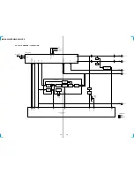
Page 19: ... D A CONVERTER IC101 INPUT INTERFACE DIGITAL FILTER NOISE SHAPER D A COMVERTER 4 DEMODULATOR 21 70 71 18 LEVEL 14 57 C6500R C6500RX C6500R C6500RX MUTING Q181 MUTING Q271 MUTING Q171 62 63 BATTERY OFF MUTE DRIVER Q621 C6500R C6500RX BACK UP B D622 D502 D302 X501 3 68MHz X502 32 768kHz RESET RESET EMPHASIS I H C INPUT MULTIPLEXER LOUDNESS MUTE MONO FADER MIXER OUTLF OUTLR R CH OUTPUT SELECTOR AM FM...

Page 20: ...TROL SWITCH Q633 FU601 COM 8V AUDIO CIRCUIT B 05 RST 3 BATT BATTERY SWITCH 10 BU IN UNISI 50 UNISO UNICKIO MDMON 10 77 3 19 UNICKO 17 UNISI 18 UNISO 86 HSTX 11 24 SIRCS 90 65 MD ON D301 D708 TH701 D702 D701 D662 LED810 LSW810 LED810 MD DISC SLOT VCC TUNER 5 6V RDS DECODER IC51 B TUNER 8 7V VCC 7 7 ACC REGULATOR Q631 12V REGULATOR Q361 3 3V REGULATOR IC401 Q401 5V REGULATOR Q362 B SWITCH Q402 403 3...

Page 21: ...te on Schematic Diagram All capacitors are in µF unless otherwise noted pF µµF 50 WV or less are not indicated except for electrolytics and tantalums All resistors are in Ω and 1 4 W or less unless otherwise specified indicates tolerance f internal component C panel designation U B Line Power voltage is dc 14 4V and fed with regulated dc power supply from ACC and BATT cords Voltages are taken with...

Page 22: ...101 IC503 IC502 IC401 IC305 L304 L303 L305 L306 Q401 L101 L102 D501 D401 K A R350 CN102 20 1 1 12 36 25 24 13 37 48 Q302 B C E L302 X501 X301 C106 C109 B C E K A C318 C319 C346 CHASSIS CHASSIS 05 OPTICAL PICK UP BLOCK KMS 241C CHASSIS 1 2 65 64 80 1 CN101 CN103 29 30 1 675 655 11 11 CHASSIS 1 654 693 11 SENSOR FLEXIBLE BOARD A MAIN BOARD CN301 SERVO BOARD COMPONENT SIDE 41 40 24 25 1 A 2 3 4 5 6 7...

Page 23: ... R333 R335 R512 R510 R540 R542 R520 R521 R359 Q402 B C E B C E Q403 C333 RB301 RB302 TH501 RB503 IC307 L501 L301 1 5 9 13 26 22 18 14 C361 C102 C202 C344 C351 1 675 655 11 11 SERVO BOARD CONDUCTOR SIDE C506 05 1 A 2 3 4 5 6 7 8 9 10 11 12 B C D E F G H I J K 4 7 PRINTED WIRING BOARD SERVO Board Conductor Side See page 21 for Circuit Boards Location Semiconductor Location Ref No Location IC307 C 10...

Page 24: ...Waveforms See page 36 for IC Block Diagrams Voltages and waveforms are dc with respect to ground under no signal conditions no mark MD PLAY Impossible to measure The components identified by mark 0 or dotted line with mark 0 are critical for safety Replace only with part number specified ...

Page 25: ...25 25 4 9 SCHEMATIC DIAGRAM SERVO Board 2 2 See page 31 for Waveforms See page 36 for IC Block Diagram Voltages and waveforms are dc with respect to ground under no signal conditions no mark MD PLAY Impossible to measure Page 29 ...

Page 26: ...I 7 D661 D 5 D662 D 5 D673 C 5 D674 C 5 D701 E 5 D702 C 4 D703 B 3 D704 B 2 D705 B 2 D706 B 2 D708 G 7 D710 D 4 IC51 I 12 IC90 G 11 IC151 D 10 IC501 I 5 IC652 J 3 IC701 C 3 Q1 G 11 Q111 E 12 Q131 F 12 Q171 B 11 Q181 B 11 Q250 H 2 Q271 C 11 Q281 C 11 Q363 I 3 Q551 J 6 Q571 D 5 Q621 C 10 Q622 C 9 Q633 J 2 Q651 I 8 Q652 I 8 Q661 D 5 Q701 D 5 Q704 G 7 Q705 C 4 Q706 D 4 4 10 PRINTED WIRING BOARD MAIN B...

Page 27: ... I 4 D676 I 4 D677 I 4 D709 G 5 IC611 A 7 IC671 F 1 Q90 G 11 Q121 E 12 Q361 H 1 Q362 G 1 Q631 J 2 5 4 8 7 6 2 1 3 FRONT VIEW 9 10 11 12 13 14 15 16 1 2 3 4 5 6 7 8 RL FL FR RL FR BATT GND BATT RR RL FL RL FL FR RR FL RL RR FR ANT REM AMP REM ACC ACC ANT REM GND ATT Semiconductor Location Ref No Location 4 11 PRINTED WIRING BOARD MAIN Board Conductor Side See page 21 for Circuit Boards Location Pag...

Page 28: ...X 28 28 4 12 SCHEMATIC DIAGRAM MAIN Board 1 3 See page 31 for Waveform See page 36 for IC Block Diagrams Voltages and waveforms are dc with respect to ground under no signal detuned conditions no mark FM MW LW Page 29 Page 30 ...

Page 29: ...29 29 Voltages and waveforms are dc with respect to ground under no signal detuned conditions no mark FM MW LW MD PLAY Impossible to measure 4 13 SCHEMATIC DIAGRAM MAIN Board 2 3 See page 31 for Waveforms Page 25 Page 28 Page 30 ...

Page 30: ...R C6500R C6500RX 30 30 4 14 SCHEMATIC DIAGRAM MAIN Board 3 3 See page 36 for IC Block Diagrams Voltages are dc with respect to ground under no signal detuned conditions no mark FM MD PLAY Page 28 Page 29 Page 33 ...

Page 31: ...lay Mode qd IC304 3 MD Play Mode qf IC304 7 MD Play Mode qg IC501 ea EXTAL 6 IC301 wh XBCK MD Play Mode 4 4 Vp p 88 ns 4 6 Vp p 354 ns Apporx 0 6 Vp p 3 8 Vp p 22 7 µs 4 4 Vp p 88 ns 3 4 Vp p 354 ns Apporx 1 5 Vp p 4 IC301 qh OSCI MD Play Mode 5 IC301 wg LRCK MD Play Mode 4 6 Vp p 44 3 ns 4 4 Vp p 22 7 µs Approx 0 5 Vp p Approx 2 Vp p 4 1 Vp p 44 3 ns 3 4 Vp p 44 3 ns 4 4 Vp p 44 3 ns 3 7 Vp p 101...

Page 32: ...MDX C6400R C6500R C6500RX 32 32 4 15 PRINTED WIRING BOARD SUB Board See page 21 for Circuit Boards Location Page 27 Page 34 ...

Page 33: ...MDX C6400R C6500R C6500RX 33 33 4 16 SCHEMATIC DIAGRAM SUB Board Page 30 Page 35 ...

Page 34: ... Boards Location Semiconductor Location Ref No Location IC951 C 5 LED901 A 2 LED902 C 2 LED903 C 3 LED904 A 3 LED910 B 12 LED911 B 12 LED912 A 12 LED913 A 5 LED914 B 5 LED915 B 5 Semiconductor Location Ref No Location D901 A 11 D902 B 10 D903 B 10 D904 B 10 D951 C 4 D952 B 6 IC901 B 8 Page 32 ...

Page 35: ...MDX C6400R C6500R C6500RX 35 35 4 18 SCHEMATIC DIAGRAM KEY Board See page 31 for Waveform Voltages and waveforms are dc with respect to ground under no signal detuned conditions no mark FM Page 33 ...

Page 36: ...19 NC 18 XTSL 17 OSCO 16 OSCI 15 TX 14 XINT 13 RECP 12 DQSY 11 SQSY 10 XRST 9 SENS 8 SRDT 7 XLAT 6 SCLK 5 SWDT 4 MNT3 3 MNT2 2 MNT1 1 MNT0 PWM GENERATOR AUTO SEQUENCER SERVO DSP CPU I F MONITOR CONTROL SPINDLE SERVO EACH BLOCK EACH BLOCK DIGITAL AUDIO I F SAMPLING RATE CONVERTER CLOCK GENERATOR SUBCODE PROCESSOR EACH BLOCK A D CONVERTER ANALOG MUX EFM ACIRC ENCODER DECODER PLL SHOCK RESISTANT MEMO...

Page 37: ...E PREDRIVE AMP INTERFACE AMP AMP AMP VDD PSB AMP 1 2 3 4 OUT1 VM VCC FIN 8 7 6 5 GND OUT2 VREF RIN CONTROL LOGIC TSD POWER SAVE DRIVER DRIVER IC307 MN41V4400TT 08S DATA BUS DQ3 DQ4 VSS 3 DQ2 2 A9 5 A0 9 A1 10 A2 11 A3 12 VCC 13 NC 6 NC 7 NC 8 DQ1 1 26 23 24 25 A8 NC NC NC 19 20 21 A6 A7 17 18 A4 A5 15 14 16 ROW DECODERS WORD DRIVERS MEMORY CELLS INTERNAL ADDRESS COUNTER TIMING GENERATOR TIMING GEN...

Page 38: ... POWER SUPPLY RESET TEST CONTROL OSCILLATOR CLOCK PAUSE DETECTOR MULTI PATH DETECTOR 57kHz 8th ORDER BAND PASS FILTER RDS RDBS DECODER RDS RDBS DEMODULATOR IIC BUS SLAVE TRANSCEIVER 17 18 CIN 19 LVIN 20 8 7 DATA CLOCK DATA CLOCK 4 4 5 9 10 3 4 5 IC671 BA4908 V3 OVER VOLTAGE PROTECT REGULATOR 1 2 3 4 5 6 7 8 9 10 12 11 NC TUNER8 7 ANT SW TUNER5 6 SW STB VDD5 6V AMP VCC ANT COM8 7V TUNER5 6V TUNER8 ...

Page 39: ...TOR D A CONVERTER PILOT CANCELATION PIL DET PLL AM FM NOISE BLANKER BEEP 80kHz LP 17 PULSE FORMER QUAL SUPPLY SECOND MAIN ACIN MONO FADER MONO FADER MONO FADER MONO FADER MONO FADER MONO FADER SUBWOOFER PHASE CONTROL MIXER OUTPUT SELECTOR FRONT REAR SW VDD SCL SDA GND SM QUAL MPOUT MPIN LEVEL MPX AMIF SEL SER FD1L FD1L FD1R FD1R FD2L FD2L FD2R FD2R AM ACINLF SWINR SWINL ACOUTR ACOUTL CREF MUX MD1 ...

Page 40: ...tic head on off output Not used fixed at L 16 OSCI I System clock signal 512Fs 22 5792 MHz input from the oscillator circuit 17 OSCO O System clock signal 512Fs 22 5792 MHz output terminal Not used open 18 XTSL I Input terminal for the system clock frequency setting L 45 1584 MHz H 22 5792 MHz fixed at H in this set 19 RVDD Power supply terminal 3 3V digital system 20 RVSS Ground terminal digital ...

Page 41: ...e CXA2523AR IC302 68 ADIO O A Monitor output of the A D converter input signal Not used open 69 AVDD Power supply terminal 3 3V analog system 70 ADRT I A A D converter operational range upper limit voltage input terminal fixed at H in this set 71 ADRB I A A D converter operational range lower limit voltage input terminal fixed at L in this set 72 AVSS Ground terminal analog system 73 SE I A Sled e...

Page 42: ... signal output to the BH6511FS IC303 93 SPRD O Spindle servo drive PWM signal output to the BH6511FS IC303 94 SPFD O Spindle servo drive PWM signal output to the BH6511FS IC303 95 FGIN I Not used fixed at L 96 TEST1 I 97 TEST2 I Input terminal for the test fixed at L 98 TEST3 I 99 DVSS Ground terminal digital system 100 EFMO O EFM signal output terminal when recording mode Not used open I A for an...

Page 43: ...l circuit BPF3T 24 VCC Power supply terminal 3 3V 25 WBLADJ I Center frequency setting terminal for the internal circuit BPF22 26 TE O Tracking error signal output to the CXD2652AR IC301 27 CSLED I Connected to the external capacitor for low pass filter of the sled error signal 28 SE O Sled error signal output to the CXD2652AR IC301 29 ADFM O FM signal output of the ADIP 30 ADIN I Receives a ADIP ...

Page 44: ... 4M bit external D RAM H 2M bit internal D RAM of CXD2652AR fixed at L in this set 24 25 NCO O Not used open 26 MNT0 I Focus OK signal input from the CXD2652AR IC301 H is input when focus is on L NG 27 MNT1 I Track jump detection signal input from the CXD2652AR IC301 28 MNT2 I Busy monitor signal input from the CXD2652AR IC301 29 MNT3 I Spindle servo lock status monitor signal input from the CXD26...

Page 45: ...he SONY bus interface IC600 and battery check circuit H battery on 61 BUS ON I SONY bus on off control signal input from the master controller IC700 L bus on 62 SQSY I Subcode Q sync SCOR input from the CXD2652AR IC301 L is input every 13 3 msec Almost all H is input 63 C SW I Inputs the disc loading start or disc eject completion detect switch detection signal L When start or eject completed of t...

Page 46: ... data input from the SONY bus interface IC701 18 UNISO O Serial data output to the SONY bus interface IC701 19 UNICKO O Serial clock signal output to the MD mechanism controller IC501 and SONY bus interface IC701 20 UNICKI I Serial clock signal input from the MD mechanism controller IC501 for SONY bus 21 CD MD I Setting terminal for the internal mechanism CD or MD L CD H MD fixed at H in this set ...

Page 47: ... muting on off control signal output terminal H muting on 59 AMPON O Standby on off control signal output to the power amplifier IC611 L standby mode H ampifier on 60 AMPATT O Power amplifier muting on off control signal output to the power amplifier IC611 L muting on 61 COLSW I Setting terminal for the illumination color L 2 color H 1 color fixed at H in this set 62 COLSEL I Setting terminal for ...

Page 48: ...ting terminal for the internal mechanism tape or CD L CD H tape fixed at L in this set 100 101 NCO O Not used open 102 AMTL IN I Auto metal detection signal input terminal L auto metal Not used open 103 AMS IN I Input terminal of whether a music is present or not is detected at auto music sensor L music is present H music is not present Not used open 104 REEL I Rotation detect signal input termina...

Page 49: ...alid at L input At normal mode dolby on off control signal output terminal dolby on at H output Not used this function open 117 TAPATT O Audio signal select control signal output terminal Not used open 118 NCO O Not used open 119 VSS Ground terminal 120 PW ON O Main system power supply on off control signal output to the BA4908 IC671 H power on ...

Page 50: ...ts Color Cabinet s Color Ref No Part No Description Remark Ref No Part No Description Remark 1 X 3378 458 1 PANEL ASSY SUB 2 X 3376 699 2 GEAR ASSY 3 3 030 909 02 DAMPER OIL 4 3 713 786 51 SCREW P 2X3 5 3 034 086 01 SPRING DOOR 6 3 033 750 02 DOOR MD 7 3 040 990 01 BUTTON EJECT Z 8 1 677 057 11 SUB BOARD 9 A 3294 867 A MAIN BOARD COMPLETE C6400R 9 A 3294 868 A MAIN BOARD COMPLETE C6500RX 9 A 3294 ...

Page 51: ...B VOL 59 3 040 997 01 PLATE LCD GROUND 60 1 694 660 11 CONDUCTIVE BOARD CONNECTION 61 3 041 371 01 SHEET REFLECTOR 62 3 040 993 01 PLATE LCD LIGHT GUIDE 63 3 040 992 01 HOLDER LCD 64 X 3378 398 1 PANEL ASSY FRONT BACK 65 3 935 151 01 SPRING OPEN 66 3 040 989 01 BUTTON OPEN 67 3 041 005 11 BUTTON D D BASS 68 3 041 006 01 BUTTON AF TA 69 X 3378 685 1 FRONT PANEL SV ASSY C6500R 69 X 3378 686 1 FRONT ...

Page 52: ...714 02 SPRING FLOAT F TENSION 104 3 921 111 01 SPRING FLOAT B TENSION 105 3 919 273 01 DAMPER OIL 106 X 3376 796 3 HOLDER ASSY 107 3 032 682 01 SPRING HOLDER 108 3 034 301 01 CUSHION EJ2 109 3 034 302 01 CUSHION EJ3 110 3 032 712 01 LEVER LOCK R 111 3 919 281 01 SPRING CHUCKING 112 X 3376 800 1 COVER ASSY MD 113 3 035 932 01 WASHER STOPPER 114 X 3376 797 3 LEVER LE ASSY 115 3 032 707 01 SPRING LEV...

Page 53: ...ark Ref No Part No Description Remark 161 X 3373 213 1 SCREW ASSY FEED 162 3 939 590 07 SCREW IB LOCK 163 3 010 091 01 SPRING SL FEED 164 3 919 293 01 SHAFT OPT S GUIDE 0165 8 583 065 03 OPTICAL PICK UP KMS 241C J1RP 166 3 920 537 01 SHAFT OPT L GUIDE M901 A 3301 407 A MOTOR ASSY SP SPINDLE M902 A 3291 190 A MOTOR ASSY SL SLED M903 A 3291 191 A MOTOR ASSY LO LOADING M902 M901 M903 7 7 8 9 9 8 157 ...

Page 54: ... 906 11 DISPLAY PANEL LIQUID CRYSTAL C6400R C6500R LCD901 1 803 906 31 DISPLAY PANEL LIQUID CRYSTAL C6500RX LED LED901 8 719 038 03 LED CL 190Y CD T ILLUMINATION AMBER LED901 8 719 038 07 LED CL 190PG CD T ILLUMINATION GREEN LED901 8 719 061 16 LED CL 190SR CD T ILLUMINATION RED LED902 8 719 038 03 LED CL 190Y CD T ILLUMINATION AMBER LED902 8 719 038 07 LED CL 190PG CD T ILLUMINATION GREEN LED902 ...

Page 55: ...AL CHIP 680 0 5 1 10W R903 1 216 647 11 METAL CHIP 680 0 5 1 10W R904 1 216 651 11 METAL CHIP 1K 0 5 1 10W R905 1 216 655 11 METAL CHIP 1 5K 0 5 1 10W R906 1 216 655 11 METAL CHIP 1 5K 0 5 1 10W R907 1 216 659 11 METAL CHIP 2 2K 0 5 1 10W R908 1 216 663 11 METAL CHIP 3 3K 0 5 1 10W R909 1 216 667 11 METAL CHIP 4 7K 0 5 1 10W R910 1 216 671 11 METAL CHIP 6 8K 0 5 1 10W R911 1 208 806 11 RES CHIP 10...

Page 56: ...1uF 10 25V C98 1 164 004 11 CERAMIC CHIP 0 1uF 10 25V C101 1 126 160 11 ELECT 1uF 20 50V C110 1 163 251 11 CERAMIC CHIP 100PF 5 50V C111 1 109 982 11 CERAMIC CHIP 1uF 10 10V C113 1 109 982 11 CERAMIC CHIP 1uF 10 10V C121 1 164 004 11 CERAMIC CHIP 0 1uF 10 25V C122 1 163 037 11 CERAMIC CHIP 0 022uF 10 25V C123 1 163 037 11 CERAMIC CHIP 0 022uF 10 25V C131 1 124 233 11 ELECT 10uF 20 16V C141 1 163 2...

Page 57: ...1 1 580 907 31 PLUG CONNECTOR BUS CONTROL IN JACK CNJ151 1 774 699 12 JACK PIN 4P BUS AUDIO IN AUDIO OUT C6400R CNJ151 1 774 700 11 JACK PIN 6P BUS AUDIO IN AUDIO OUT REAR FRONT C6500R C6500RX DIODE D1 8 719 073 01 DIODE MA111 TX D2 8 719 067 56 DIODE MA112 TX D90 8 719 073 01 DIODE MA111 TX D91 8 719 073 01 DIODE MA111 TX D92 8 719 976 99 DIODE UDZ TE 17 5 1B D131 8 719 422 12 DIODE UDZ TE 17 3 9...

Page 58: ... 729 920 21 TRANSISTOR DTC314TK T 146 Q281 8 729 920 21 TRANSISTOR DTC314TK T 146 Q361 8 729 019 00 TRANSISTOR 2SD2394 G Q362 8 729 019 00 TRANSISTOR 2SD2394 G Q363 8 729 921 25 TRANSISTOR FMC2 T148 Q551 8 729 921 25 TRANSISTOR FMC2 T148 Q571 8 729 120 28 TRANSISTOR 2SC2412K T 146 QR C6500R C6500RX Q621 8 729 027 23 TRANSISTOR DTA114EKA T146 Q622 8 729 021 94 FET 2SK1657 T1B Q631 8 729 423 99 TRAN...

Page 59: ... 10W R545 1 216 097 00 RES CHIP 100K 5 1 10W R546 1 216 097 00 RES CHIP 100K 5 1 10W R547 1 216 097 00 RES CHIP 100K 5 1 10W R551 1 249 409 11 CARBON 220 5 1 4W C6400R C6500R R551 1 249 413 11 CARBON 470 5 1 4W C6500RX R552 1 216 025 00 RES CHIP 100 5 1 10W R553 1 216 025 00 RES CHIP 100 5 1 10W R554 1 216 025 00 RES CHIP 100 5 1 10W R555 1 216 025 00 RES CHIP 100 5 1 10W R556 1 216 025 00 RES CHI...

Page 60: ... 1 109 982 11 CERAMIC CHIP 1uF 10 10V C328 1 162 966 11 CERAMIC CHIP 0 0022uF 10 50V C329 1 164 227 11 CERAMIC CHIP 0 022uF 10 25V C330 1 162 970 11 CERAMIC CHIP 0 01uF 10 25V C331 1 107 826 11 CERAMIC CHIP 0 1uF 10 16V C333 1 107 826 11 CERAMIC CHIP 0 1uF 10 16V C334 1 164 004 11 CERAMIC CHIP 0 1uF 10 25V C335 1 164 004 11 CERAMIC CHIP 0 1uF 10 25V C336 1 162 970 11 CERAMIC CHIP 0 01uF 10 25V C33...

Page 61: ... 1 16W R327 1 216 821 11 METAL CHIP 1K 5 1 16W R328 1 216 811 11 METAL CHIP 150 5 1 16W R329 1 216 819 11 METAL CHIP 680 5 1 16W R330 1 216 853 11 METAL CHIP 470K 5 1 16W R331 1 216 809 11 METAL CHIP 100 5 1 16W R332 1 216 809 11 METAL CHIP 100 5 1 16W R333 1 216 819 11 METAL CHIP 680 5 1 16W R334 1 216 809 11 METAL CHIP 100 5 1 16W R335 1 216 815 11 METAL CHIP 330 5 1 16W R336 1 216 853 11 METAL ...

Page 62: ...00R SWITCH LSW810 1 771 609 11 SWITCH TACTILE WITH LED Z C6400R C6500R LSW810 1 771 883 21 SWITCH TACTILE WITH LED Z C6500RX MISCELLANEOUS 17 1 776 527 51 CORD WITH CONNECTOR ISO POWER C6400R 17 1 776 527 61 CORD WITH CONNECTOR ISO POWER C6500R C6500RX 60 1 694 660 11 CONDUCTIVE BOARD CONNECTION 153 1 654 693 11 SENSOR FLEXIBLE BOARD 0165 8 583 065 03 OPTICAL PICK UP KMS 241C J1RP CNP811 1 792 195...

Page 63: ...07 POWER CORD 1 PARTS FOR INSTALLATION AND CONNECTION 501 1 465 459 21 ADAPTER ANTENNA 502 3 012 360 31 FRAME 503 3 040 979 01 COLLAR 504 3 233 644 01 SPRING FITTING 505 3 934 325 01 SCREW K 5X8 TAPPING 506 X 3366 405 1 SCREW ASSY EXP FITTING 507 1 776 527 51 CORD WITH CONNECTOR ISO POWER C6400R 507 1 776 527 61 CORD WITH CONNECTOR ISO POWER C6500R C6500RX 504 Ver 1 1 2001 05 ...

Page 64: ...icking the version at the upper right on the revised page allows you to jump to the next revised page Ver Date Description of Revision 1 2 2001 12 Change of Part No for TU1 RPC 01002 1 1 2001 05 Change of Part No for SPRING FITTING ECN CSA04727 1 0 2000 02 New MDX C6400R C6500R C6500RX ...

Reviews: