background image

13

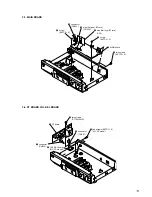
3-3. MAIN BOARD

3-4. PT BOARD, VOL-SEL BOARD

4

 two screws
(BVTP3 

×

 8)

6

screw
(BVTP3 

×

 8)

5

screw
(BVTP3 

×

 8)

3

connector
(CN902)

2

wire (flat type) (23core)
(CN400)

1

wire (flat type) (27core)
(CN1)

7

MAIN board

1

connector
(CN900)

2

connector
(CN951)

3

two screws
(PTTWH (M3))

5

two screws (BVTP3 

×

 8)

4

PT board

6

VOL-SEL board
(MY, SP model)

(MY, SP model)

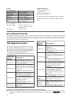
Summary of Contents for MDS-JE440 - Md Player

Page 1: ...ser diode Material GaAlAs Revolutions CLV 400 rpm to 900 rpm Error correction ACIRC Advanced Cross Interleave Reed Solomon Code Sampling frequency 44 1 kHz Coding ATRAC Adaptive TRansform Acoustic Coding ATRAC 3 Modulation system EFM Eight to Fourteen Modulation Number of channels 2 stereo channels Frequency response 5 to 20 000 Hz 0 3 dB Signal to noiseratio Over 96 dB during play Wow and flutter...

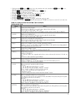
Page 2: ...d MD is dirty with smudges fingerprints etc scratched or substandard in quality Replace the disc and repeat the recording procedure C13 Read Error The deck could not read the TOC on the MD properly Take out the MD and insert it again C14 Toc Error The deck could not read the TOC on the MD properly Insert another disc If possible erase all the tracks on the MD page 32 C41 Cannot Copy The sound sour...

Page 3: ...cording and playback Displays r xx p yy xx is the number of errors during recording yy is the number of errors during playback This is displayed in hexadecimal from 00 to FF Displays the total number of errors Displays total xx This is displayed in hexadecimal from 00 to FF Displays the past ten errors Displays 0x ErrCd X is the history number The younger the number the more recent is the history ...

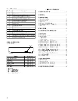
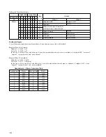
Page 4: ...ms 46 6 15 IC Pin Functions 48 7 EXPLODED VIEWS 7 1 Chassis Section 54 7 2 Front Panel Section 55 7 3 Mechanism Section 1 MDM 7A 56 7 4 Mechanism Section 2 MDM 7A 57 8 ELECTRICAL PARTS LIST 58 Table of Error Codes Error Code 10 12 20 21 22 23 24 30 31 40 41 42 43 50 51 Could not load Loading switches combined incorrectly Timed out without reading the top of PTOC Could read top of PTOC but detected...

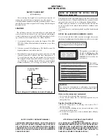
Page 5: ... TO SAFE OPERATION REPLACE THESE COMPONENTS WITH SONY PARTS WHOSE PART NUMBERS APPEAR AS SHOWN IN THIS MANUAL OR IN SUPPLEMENTS PUBLISHED BY SONY ATTENTION AU COMPOSANT AYANT RAPPORT À LA SÉCURITÉ LES COMPOSANTS IDENTIFÉS PAR UNE MARQUE 0 SUR LES DIAGRAMMES SCHÉMATIQUES ET LA LISTE DES PIÈCES SONT CRITIQUES POUR LA SÉCURITÉ DE FONCTIONNEMENT NE REMPLACER CES COMPOSANTS QUE PAR DES PIÈSES SONY DONT...

Page 6: ...ollows GND Ground I 3V For measuring IOP Check the deterioration of the optical pick up laser IOP For measuring IOP Check the deterioration of the optical pick up laser TE TRK error signal Traverse adjustment VC Reference level for checking the signal RF RF signal Check jitter FE Focus error signal I 3V Iop GND TE FE VC RF I 3V IOP GND TE FE VC RF 1 7 for MDM 7A I 3V CN105 IOP TE VC GND FE RF ...

Page 7: ... changed will blink 5 Input the Iop value written on the optical pick up To select the number Rotate the l AMS L knob To select the digit Press the l AMS L knob 6 When the YES button is pressed the display becomes Measu is an arbitrary number 7 As the adjustment results are recorded for the 6 value Leave it as it is and press the YES button 8 Complete will be displayed momentarily The value will b...

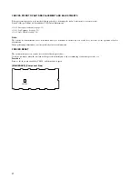
Page 8: ...e 24 Note The criteria for determination above is intended merely to determine if satisfactory or not and does not serve as the specified value for adjustments When performing adjustments use the specified values for adjustments FORCED RESET The system microprocessor can be reset in the following procedure Use these procedure when the unit cannot be operated normally due to the overrunning of the ...

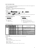
Page 9: ... plug from the outlet If the test mode cannot be exited refer to Forced Reset on page 8 Fig 1 Reading the Test Mode Display During recording and stop RTs c c Fluorescent display tube display Address Physical address on disc Hexadecimal Bit Binary Higher Bits Lower Bits 8 4 2 1 8 4 2 1 b7 b6 b5 b4 b3 b2 b1 b0 0 0 0 0 0 0 0 1 0 0 0 0 0 0 1 0 0 0 0 0 0 1 0 0 0 0 0 0 1 0 0 0 0 0 0 1 0 0 0 0 0 0 1 0 0 ...

Page 10: ...e than two causes they will be added Example When 84 is displayed Higher bit 8 1000 t b7 Lower bit 4 0100 t b2 In this case as b2 and b7 are 1 and others are 0 it can be determined that the retry cause is combined of emphasis OFF monaural original copyright exists and write allowed Example When 07 is displayed Higher bit 0 1000 t All 0 Lower bit 7 0111 t b0 b1 b2 In this case as b0 b1 and b2 are 1...

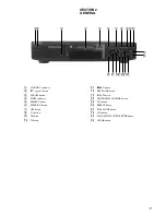
Page 11: ...button 6 MENU NO button 7 YES button 8 H button 9 S button q s button qa z REC button qs REC MODE button qd INPUT button qf LEVEL DISPLAY CHAR button qg J button qh REPEAT button qj PLAY MODE button qk j button ql l AMS L PUSH ENTER button w CLEAR button 12 3 4 5 6 7 8 9 0 qa ql w qf qg qh qj qs qd qk ...

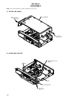
Page 12: ...226 3 2 FRONT PANEL SECTION Note Follow the disassembly procedure in the numerical order given 1 two screws CASE 3 TP2 2 case 408226 1 two screws CASE 3 TP2 1 wire flat type 17core CN490 2 five screws BVTP3 8 3 claw 4 front panel section 3 claw ...

Page 13: ... BVTP3 8 6 screw BVTP3 8 5 screw BVTP3 8 3 connector CN902 2 wire flat type 23core CN400 1 wire flat type 27core CN1 7 MAIN board 1 connector CN900 2 connector CN951 3 two screws PTTWH M3 5 two screws BVTP3 8 4 PT board 6 VOL SEL board MY SP model MY SP model ...

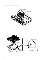
Page 14: ...tep screws BVTTWH M3 1 harness 4 mechanism deck 3 M102 M101 M103 S102 2Remove the solder Two portion 2Remove the solder Two portion 2Remove the solder Two portion 2Remove the solder Three portion 1connector CN104 5connector CN101 3two screws BTP 2 6 4BD board ...

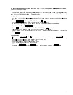
Page 15: ...tment EF MO ADJUS When pressing the z REC button 4 2 SETTING THE TEST MODE The following are two methods of entering the test mode Procedure 1 While pressing the AMS knob and x button connect the power plug to an outlet and release the AMS knob and x button When the test mode is set Check will be displayed Rotating the AMS knob switches between the following three groups y Check y Service y Develo...

Page 16: ...tc Continuous playback mode Continuous recording mode 4 5 SELECTING THE TEST MODE There are 25 types of test modes as shown below The groups can be switched by rotating the AMS knob After selecting the group to be used press the YES button After setting a certain group rotating the AMS knob switches between these modes Refer to Group in the table for details selected All adjustments and checks dur...

Page 17: ... palyback check 1 Entering the continuous recording mode 1 Set a recordable disc in the unit 2 Rotate the AMS knob and display CREC1 MODE C35 3 Press the YES button to change the display to CREC1 MID 4 When access completes the display changes to CREC1 and REC lights up Note The numbers displayed shows you the recording position addresses 2 Changing the parts to be recorded 1 When the YES button i...

Page 18: ...n CPLAY and CREC are started the display will forcibly be switched to the error rate display as the initial mode 1 Mode display Displays TEMP ADJUST CPLAY1MODE etc 2 Error rate display Displays the error rate in the following way C1 AD C1 Indicates the C1 error AD Indicates ADER 3 Address display The address is displayed as follows MO recordable disc CD playback only disc If the LEVEL DISPLAY CHAR...

Page 19: ...the disc loaded at step 2 will be ejected DISC IN will be displayed Load the check disc MD TDYS 1 5 When the disc is loaded in step 4 the check will automatically be resumed from 07 CHECK 6 After completing to test item 12 check OK or NG will be displayed If all items are OK CHECKALL OK will be displayed If any item is NG it will be displayed as NG xxxx When CHECK ALL OK is displayed it means that...

Page 20: ...ick up such as sound skipping are suspected follow the following check Check before replacement Other faults are suspected Check the threading mechanism etc Start NG NG NG OK OK OK Laser Power Check 5 6 2 See page 23 5 6 3 See page 23 5 6 4 See page 24 Iop Compare Auto Check Replace Optical pick up or MDM 7A ...

Page 21: ...ter turning off and then on the power initialize the EEPROM For details refer to 4 11 WHEN MEMORY NG IS DISPLAYED See page 19 Abbreviation OP Optical pick up 5 7 INITIAL SETTING OF ADJUSTMENT VALUE See page 26 5 9 TEMPERATURE COMPENSATION OFFSET ADJUSTMENT See page 26 5 10 LASER POWER ADJUSTMENT See page 26 5 12 TRAVERSE ADJUSTMENT See page 27 5 13 FOCUS BIAS ADJUSTMENT See page 28 5 16 AUTO GAIN ...

Page 22: ...and checks with in the order shown in the following table 2 Set the test mode when performing adjustments After completing the adjustments exit the test mode Perform the adjustments and checks in group S of the test mode 3 Perform the adjustments to be needed in the order shown 4 Use the following tools and measuring devices Check Disc MD TDYS 1 Parts No 4 963 646 01 Test Disk MDW 74 GA 1 Parts No...

Page 23: ...r reading Optical pick up displayed value 10 Optical pick up label 5 Press the MENU NO button and display LDPWR CHECK and stop the laser emission The MENU NO button is effective at all times to stop the laser emission For details of the method for checking this value refer to 5 8 Recording and Displaying Iop Information Note 1 After step 4 each time the YES button is pressed the display will be sw...

Page 24: ... 2 the check will start automatically 4 When XX CHECK is displayed the item corresponding to XX will be performed When 06 CHECK completes the disc loaded at step 2 will be ejected DISC IN will be displayed Load the check disc MD TDYS 1 5 When the disc is loaded the check will automatically be resumed from 07 CHECK 6 After completing to test item 12 check OK or NG will be displayed If all items are...

Page 25: ... 2 10 Press the MENU NO button to stop playback and press the A button and remove the disc 330 kΩ Oscilloscope 10pF BD board CN105 pin 4 TE CN105 pin 6 VC 5 6 7 Focus Bias Check Change the focus bias and check the focus tolerance amount Checking Procedure 1 Load a continuously recorded test disc MDW 74 GA 1 Refer to 5 5 Using the Continuously Recorded Disc 2 Rotate the AMS knob and display CPLAY1 ...

Page 26: ...ment 3 To end press the AMS button or MENU NO button to display Iop Read 5 9 TEMPERATURE COMPENSATION OFFSET ADJUTMENT Save the temperature data at that time in the non volatile memory as 25 C reference data Note 1 Usually do not perform this adjustment 2 Perform this adjustment in an ambient temperature of 22 C to 28 C Perform it immediately after the power is turned on when the internal temperat...

Page 27: ...er READ power Focus servo ON tracking servo OFF spindle S servo ON 6 Rotate the AMS knob so that the waveform of the oscilloscope becomes the specified value When the AMS knob is rotated the of EFB changes and the waveform changes In this adjustment waveform var ies at intervals of approx 2 Adjust the waveform so that the specified value is satisfied as much as possible Read power traverse adjustm...

Page 28: ...seen more clearly 5 13 FOCUS BIAS ADJUSTMENT Adjusting Procedure 1 Load a test disk MDW 74 GA 1 2 Rotate the AMS knob and display CPLAY1 MODE 3 Press the YES button and display CPLAY1 MID 4 Press the MENU NO button when C1 AD is displayed 5 Rotate the AMS knob and display FBIAS ADJUST 6 Press the YES button and display a The first four digits indicate the C1 error rate the two digits after indicat...

Page 29: ... 2 7 Press the YES button and display b Check that the C1 error is below 100 and ADER is below 2 8 Press the YES button and display a Check that the C1 error is below 100 and ADER is below 2 9 Press the MENU NO button next press the A button and remove the continuously recorded disc Note 1 If the C1 error and ADER are above other than the speci fied value at points a step 8 in the above or b step ...

Page 30: ...use the jig for checking the waveform Refer to Servicing Note on page 6 BD BOARD SIDE B D101 IC151 23 1 27 1 1 7 IC101 CN101 CN103 CN102 IC195 IC190 CN105 IC102 NOTE 5 17 ADJUSTING POINTS AND CONNECTING POINTS BD BOARD SIDE A ...

Page 31: ...ith aVOM Input impedance 10 MΩ Voltage variations may be noted due to normal produc tion tolerances Waveforms are taken with a oscilloscope Voltage variations may be noted due to normal produc tion tolerances Circled numbers refer to waveforms Signal path E PB j REC p PB DIGITAL OUT l REC DIGITAL IN Abbreviation CND Canadian model SP Singapore model MY Malaysia model HK Hong Kong model AUS Austral...

Page 32: ...3 A00 A09 XOE XWE XRAS XCAS OE WE RAS CAS D RAM IC153 DIN1 SYSTEM CONTROLLER IC1 1 2 HF MODULE ADDT DADT BCK LRCK Page 33 1024FS Page 33 Page 33 SWDT SCLK Page 33 LRCK REFLECT PROTECT LD LOW UNREG 5V 11 LIMIT IN OUT SW S101 LIMIT IN PLAY SW SIGNAL PATH PLAY ANALOG OUT PLAY DIGITAL OUT REC ANALOG IN REC DIGITAL IN S103 OUT SW S104 PLAY SW REC P S105 REC POSITION XBCKI LRCKI S102 REFLECT PROTECT DET...

Page 33: ...NTERFACE CONTROLLER CLOCK GENERATOR CLOCK DIVIDER CONTROL REGISTER INTERFACE BICK LRCK 5V A D D A CONVERTER IC500 B SYS 3 3V DADT BCK LRCK AINL AINR XTI DATA FL CLK FL CS FL JOG0 GND SW JOG1 P DOWN l AMS L PUSH ENTER S713 S701 706 711 712 S714 716 721 724 S726 731 A B SWDT SCLK CDTI CCLK CS PD SIRCS OSCI C769 R769 OSCO MIX AMP IC601 1 2 MIX AMP IC601 2 2 OSC IC550 LOW PASS FILTER IC260 1 2 LOW PAS...

Page 34: ...6 IC151 wk XBCK 7 IC151 o FS4 8 IC171 3 1 3Vp p 0 2Vp p 1 6Vp p 3 1Vp p 45 158 MHz 3 2Vp p 44 1 kHz 3 8Vp p 2 8224 MHz 1 0Vp p 45 158MHz 3 2Vp p 176 4kHz 1 IC1 ws XIN 2 IC550 2 3 5 3 IC500 9 XTI 4 IC500 qa LRCK 5 IC500 qs BICK 2 3Vp p 10 MHz 2 6Vp p 45 158 MHz 1 1Vp p 45 158 MHz 3 2Vp p 44 1 kHz 3 2Vp p 2 8224 MHz 1 IC760 yg OSCI 1 6Vp p 480 ns ...

Page 35: ...1 A 1 Q101 B 1 Q131 C 1 Q132 B 1 Q133 B 1 Q134 C 1 Semiconductor Location Ref No Location D181 D 3 D183 D 3 IC101 A 3 IC102 B 3 IC141 C 1 IC151 C 2 IC153 C 3 IC171 D 2 Semiconductor Location Ref No Location IC181 D 3 IC190 D 1 IC195 D 2 Q121 B 3 Q122 B 3 Q181 D 3 Q182 D 3 ...

Page 36: ...MDS JE440 36 36 6 4 SCHEMATIC DIAGRAM BD SECTION 1 2 See page 34 for Waveforms See page 46 for IC Block Diagrams See page 48 for IC Pin Functions See page 35 for Printed Wiring Board PIN FUNCTION ...

Page 37: ...MDS JE440 37 37 6 5 SCHEMATIC DIAGRAM BD SECTION 2 2 See page 34 for Waveforms See page 46 for IC Block Diagrams See page 49 for IC Pin Functions See page 35 for Printed Wiring Board PIN FUNCTION ...

Page 38: ... 6 PRINTED WIRING BOARD MAIN SECTION SIDE A Ref No Location D461 C 1 D462 C 1 D471 C 1 D472 D 1 D476 C 1 D477 C 1 D481 B 1 Semiconductor Location Ref No Location IC400 D 1 IC440 B 2 IC480 A 1 IC611 E 5 Q356 A 6 Q910 B 1 ...

Page 39: ...56 C 1 D255 C 1 D256 C 1 D401 B 7 D402 B 7 D403 B 7 D404 B 7 D412 B 6 Semiconductor Location Ref No Location D421 C 6 D422 C 6 D431 B 7 D432 B 7 D482 B 7 IC1 B 4 IC2 B 3 IC160 C 2 IC260 D 2 Ref No Location IC350 C 1 IC500 B 2 IC550 A 2 IC600 D 4 Q180 D 2 Q281 D 2 Q380 D 3 Q440 B 6 Q444 B 6 ...

Page 40: ...MDS JE440 40 40 6 8 SCHEMATIC DIAGRAM MAIN SECTION 1 3 See page 34 for Waveforms See page 52 for IC Pin Functions PIN FUNCTION ...

Page 41: ...MDS JE440 41 41 6 9 SCHEMATIC DIAGRAM MAIN SECTION 2 3 See page 34 for Waveforms See page 47 for IC Block Diagrams ...

Page 42: ...MDS JE440 42 42 6 10 SCHEMATIC DIAGRAM MAIN SECTION 3 3 See page 47 for IC Block Diagrams ...

Page 43: ...MDS JE440 43 43 6 11 PRINTED WIRING BOARD POWER SECTION ...

Page 44: ...MDS JE440 44 44 6 12 PRINTED WIRING BOARD DISPLAY SECTION ...

Page 45: ...MDS JE440 45 45 6 13 SCHEMATIC DIAGRAM DISPLAY SECTION See page 34 for Waveforms ...

Page 46: ... 56 BIAS 55 AVDD 54 ASYI 53 ASYO 52 MVCI 51 D3 68 VC 67 AUX1 66 FE 65 ABCD 64 BOTM 63 PEAK 50 D2 49 D0 48 D1 47 XWE 46 XRAS 45 A09 44 XCAS 43 XOE 42 DVSS 41 A11 40 A08 39 A07 38 A06 37 A05 36 A04 35 A10 34 A00 33 A01 32 A02 31 A03 30 DVDD 28 XBCK 29 FS256 26 DADT 27 LRCK 24 XBCKI 25 ADDT 23 LRCKI 22 DATAI 21 DOUT 20 DIN1 19 DIN0 18 XTSL 17 OSCO 16 OSCI 15 TX 14 XINT 13 RECP 12 DQSY 11 SQSY 10 XRST...

Page 47: ...OVERHEAT PROTECTION REFERENCE VOLTAGE GND ON OFF IN REFERENCE VOLTAGE OUT 3 4 1 VCOM AINR AINL 2 1 3 VREF 4 TEST 7 XTAI 9 XTALE 10 XTAO 8 SDTI 14 LRCK 11 BICK 12 SDTO 13 AGND 5 VA 6 A D CONVERTER BLOCK D A CONVERTER BLOCK CLOCK GENERATOR DIVIDER AUDIO INTERFACE CONTROLLER CDTI 15 CIF 18 CLKO 21 AOUTL 26 AOUTL 25 DGND 24 VD 23 VT 22 AOUTR 28 AOUTR 27 PD 19 M S 20 CS 17 CCLK 16 CONTROL REGISTER INTE...

Page 48: ...requency setting pin for the internal circuit BPF22 Tracking error signal output to the CXD2662R External capacitor connection pin for the sled error signal LPF Sled error signal output to the CXD2662R FM signal output of ADIP ADIP signal comparator input ADFM is connected with AC coupling External capacitor connection pin for AGC of ADIP ADIP duplex signal output to the CXD2662R I3 signal tempera...

Page 49: ...eset Subcode Q sync SCOR output to the system control L is output every 13 3 msec Almost all H is output Digital In U bit CD format or MD format subcode Q sync SCOR output to the system control Laser power switching input from the system control H Recording L Playback Interrupt status output to the system control Recording data output enable input from the system control System clock input 512Fs 2...

Page 50: ...the CXA2523AR Light amount signal input from the CXA2523AR Focus error signal input from the CXA2523AR Auxiliary A D input Middle point voltage 1 5V input from the CXA2523AR Monitor output of the A D converter input signal Not used 3V power supply Analog A D converter operational range upper limit voltage input Fixed at H A D converter operational range lower limit voltage input Fixed at L Ground ...

Page 51: ...king servo drive PWM output 3V power supply Digital Focus servo drive PWM output Focus servo drive PWM output 176 4 kHz clock signal output X tal Not used Sled servo drive PWM output Sled servo drive PWM output Spindle servo drive PWM output Spindle servo drive PWM output Test input Fixed at L Ground Digital EFM output when recording Abbreviation EFM Eight to Fourteen Modulation ...

Page 52: ...aser ON OFF control output H Laser ON 30 LIMIT IN I Detection input from the limit switch L Sled limit In H Sled limit Out 31 A1 OUT O A1 Control output 32 XINIT I Interrupt status input from CXD2662R 33 BEEP O Beep output 34 LRCKI I LR clock input 35 WR PWR O Write power ON OFF output L OFF H ON 36 IIC CLK I O IIC serial clock input output 37 IIC DATA I O IIC serial data input output 38 SWDT O Wr...

Page 53: ...gnal to the Flash ROM 91 VCC Power supply 3 3V 92 A8 O Address bus signal output to Flash ROM 93 VCC Power supply 3 3V 94 to 101 A7 to A0 LB O Address bus signal output to Flash ROM 102 to 113 D15 to D4 I O Data bus signal input output to the Flash ROM 114 K B CLK CTRL O Keyboard clock ON OFF signal output L OFF H ON 115 IIC BUSY O IIC cable connect check L Active 116 K B DATA O Keyboard data outp...

Page 54: ...21 ADAPTOR CONVERSION SP MY 017 1 770 019 11 ADAPTOR CONVERSION PLUG 3P UK HK 18 1 569 972 21 SOCKET SHORT 2P 19 9 910 999 31 RIVET DIA 3 NYLON SECTION 7 EXPLODED VIEWS NOTE XX X mean standardized parts so they may have some differences from the original one Items marked are not stocked since they are seldom required for routine service Some delay should be anticipated when ordering these items Th...

Page 55: ...20 01 SCREW 2 6X8 BVTP 58 4 228 625 01 BUTTON SUB A 59 4 977 593 11 RING DIA 50 ORNAMENTAL AEP UK CIS SP MY HK AUS 60 4 212 590 22 HOLDER FL 61 4 949 935 21 CUSHION FL 62 1 677 825 11 KEY SW BOARD 63 1 792 813 11 WIRE FLAT TYPE 15 CORE 64 A 4725 163 A DISPLAY BOARD COMPLETE US CND 64 A 4725 167 A DISPLAY BOARD COMPLETE AEP UK CIS HK AUS 64 A 4725 171 A DISPLAY BOARD COMPLETE SP MY 65 X 4952 926 1 ...

Page 56: ... 01 BELT LOADING 205 3 372 761 01 SCREW M1 7 TAPPING 206 4 227 002 01 GEAR PULLEY 207 4 226 999 01 LEVER HEAD 208 X 4952 665 1 SPRING SHT ASSY LEAF 209 4 228 923 01 LOCK HOLDER 210 4 229 533 01 SPRING STOPPER TORSION 211 4 227 012 01 SPRING HOLDER TENSION 212 4 227 019 01 PLATE HOLDER RETAINER 213 4 227 013 01 SPRING EJ TENSION 214 4 226 995 01 SLIDER EJ 215 4 226 996 01 LIMITTER EJ 216 4 226 997 ...

Page 57: ...COMPLETE 252 4 908 618 21 SCREW BTP 2X6 253 3 372 761 01 SCREW M1 7 TAPPING 254 4 226 993 01 RACK 255 4 227 014 01 SPRING RACK COMPRESSION 256 4 226 992 01 BASE SL 257 1 678 514 11 FLEXIBLE BOARD 0258 A 4672 541 A OPTICAL PICK UP KMS 260B J1N 259 4 988 560 01 SCREW P 1 7X6 260 4 996 265 01 SHAFT MAIN 261 4 226 989 01 CHASSIS 262 4 211 036 01 SCREW 1 7X2 5 PWH 263 4 226 990 01 BASE BU A 264 4 227 0...

Page 58: ...968 11 CERAMIC CHIP 0 0047uF 10 50V C166 1 125 891 11 CERAMIC CHIP 0 47uF 10 10V C167 1 164 245 11 CERAMIC CHIP 0 015uF 10 25V C169 1 164 156 11 CERAMIC CHIP 0 1uF 25V C171 1 164 156 11 CERAMIC CHIP 0 1uF 25V C172 1 164 156 11 CERAMIC CHIP 0 1uF 25V C180 1 117 370 11 CERAMIC CHIP 10uF 10V C181 1 126 206 11 ELECT CHIP 100uF 20 6 3V C182 1 163 038 91 CERAMIC CHIP 0 1uF 25V C183 1 164 156 11 CERAMIC ...

Page 59: ...1 RES CHIP 10K 5 1 16W R114 1 216 827 11 METAL CHIP 3 3K 5 1 16W R115 1 216 833 91 RES CHIP 10K 5 1 16W R116 1 216 839 11 METAL CHIP 33K 5 1 16W R117 1 216 837 11 METAL CHIP 22K 5 1 16W R118 1 218 855 11 METAL CHIP 2 2K 0 5 1 16W R119 1 218 863 11 METAL CHIP 4 7K 0 5 1 16W R120 1 218 889 11 METAL CHIP 56K 0 5 1 16W R121 1 218 863 11 METAL CHIP 4 7K 0 5 1 16W R122 1 218 855 11 METAL CHIP 2 2K 0 5 1...

Page 60: ...4W R712 1 249 421 11 CARBON 2 2K 5 1 4W F R713 1 247 843 11 CARBON 3 3K 5 1 4W R714 1 249 425 11 CARBON 4 7K 5 1 4W F R715 1 249 429 11 CARBON 10K 5 1 4W R716 1 249 435 11 CARBON 33K 5 1 4W R722 1 249 421 11 CARBON 2 2K 5 1 4W F R723 1 247 843 11 CARBON 3 3K 5 1 4W R724 1 249 425 11 CARBON 4 7K 5 1 4W F R760 1 247 807 31 CARBON 100 5 1 4W R761 1 247 807 31 CARBON 100 5 1 4W R762 1 247 807 31 CARBO...

Page 61: ...25V C408 1 104 665 11 ELECT 100uF 20 10V C410 1 162 964 11 CERAMIC CHIP 0 001uF 10 50V C411 1 164 156 11 CERAMIC CHIP 0 1uF 25V C412 1 126 963 11 ELECT 4 7uF 20 50V C413 1 162 964 11 CERAMIC CHIP 0 001uF 10 50V C431 1 104 663 11 ELECT 33uF 20 25V C443 1 162 970 11 CERAMIC CHIP 0 01uF 10 25V C447 1 126 933 11 ELECT 100uF 20 16V C461 1 126 939 11 ELECT 10000uF 20 16V C471 1 126 935 11 ELECT 470uF 20...

Page 62: ...50 1 216 864 11 METAL CHIP 0 5 1 16W R51 1 216 833 91 RES CHIP 10K 5 1 16W R52 1 216 833 91 RES CHIP 10K 5 1 16W R54 1 216 833 91 RES CHIP 10K 5 1 16W R67 1 216 833 91 RES CHIP 10K 5 1 16W R68 1 216 833 91 RES CHIP 10K 5 1 16W R69 1 216 833 91 RES CHIP 10K 5 1 16W R70 1 216 833 91 RES CHIP 10K 5 1 16W R90 1 216 845 11 METAL CHIP 100K 5 1 16W R114 1 216 845 11 METAL CHIP 100K 5 1 16W R115 1 216 833...

Page 63: ...TAL CHIP 47K 5 1 16W R1016 1 216 864 11 METAL CHIP 0 5 1 16W COMPOSITION CIRCUIT BLOCK RB102 1 236 908 11 NETWORK RESISTOR CHIP 10K RB106 1 236 908 11 NETWORK RESISTOR CHIP 10K RB110 1 236 908 11 NETWORK RESISTOR CHIP 10K RB119 1 236 908 11 NETWORK RESISTOR CHIP 10K VIBRATOR X22 1 781 174 21 VIBRATOR CERAMIC 10MHz X550 1 781 998 11 VIBRATOR CRYSTAL 45 1584MHz 1 677 826 11 PT BOARD CAPACITOR 0C900 ...

Page 64: ...AL PLUG AUDIO 60cm 1 776 263 51 CORD CONNECTION AUDIO 100cm 4 229 412 11 MANUAL INSTRUCTION SPANISH AEP 4 229 412 21 MANUAL INSTRUCTION SWEDISH DANISH FINNISH AEP 4 229 412 31 MANUAL INSTRUCTION ITALIAN AEP 4 229 412 41 MANUAL INSTRUCTION PORTUGUESE AEP 4 229 587 11 MANUAL INSTRUCTION ENGLISH US CND UK CIS SP MY AUS HK 4 229 587 21 MANUAL INSTRUCTION FRENCH GERMAN DUTCH CND AEP SP MY 4 229 587 31 ...

Reviews: