
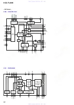


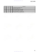


109
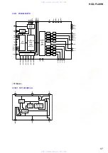
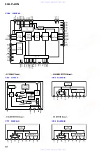
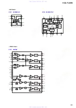
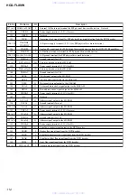
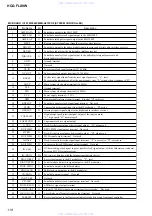
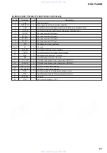
HCD-FLX9W
Pin No.
Pin Name
I/O
Description
167
XTAL
I
33.8688 MHz clock signal input terminal
168
VSS
—
Ground terminal (digital system)
169
XTA2
O
System clock output terminal (33.8688 MHz)
170
XTA1
I
System clock input terminal (33.8688 MHz)
171
VDD
—
Power supply terminal (+3.3V) (digital system)
172 to 176
D0 to D4
I/O
Two-way data bus with the mechanism controller
www. xiaoyu163. com
QQ 376315150
9
9
2
8
9
4
2
9
8
TEL 13942296513
9
9
2
8
9
4
2
9
8
0
5
1
5
1
3
6
7
3
Q
Q
TEL 13942296513 QQ 376315150 892498299
TEL 13942296513 QQ 376315150 892498299


