


92
HCD-SC5/SC6/SC8
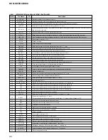
• IC901
µ
PD703033BYGF-M40-3BA-A (SYSTEM CONTROLLER)
Pin No.
1
2
3
4
5
6
7
8
9
10
11
12
13
14
15
16
17
18
19
20
21
22
23
24
25
26
27
28
29
30
31
32
33
34
35
36
37
38
39
40
41
42
43
44
45
46
47
48
I/O
O
O
I/O
O
I/O
I
O
O
—
—
O
O
O
O
I
O
I
I
I
O
—
I
O
O
I
O
—
O
O
O
O
O
O
I
I
O
—
O
I
—
—
O
O
I
O
O
O
O
Pin Name
DAMP-DATA
DAMP-CLK
I2C-DATA
CQ-RST
I2C-CLK
DSP-DO
DIG-DI
DIG-CLK
EVDD
EVSS
P-PWM
DSP-RST
DSP-PM
DSP-CS
DSP-HACN
DSP-BST
DSP-GP9
DIR-ZERO
DIR-ERR
DIR-CE
VPP
DIR-XST
DIR-AD
DIR-XMODE
DIRDO
DAMP-RST
GP12
DAMP-MUTEN
CS1
CS2
CS3
DAC-CS
AD-RST
RESET
XT1
XT2
REGC
X2
X1
VSS
VDD
CLKOUT
DIP-RST
DIP-OCP
ST-POWER
HP-MUTE
AU-MUTE
VIDEO-MUTE
Description
Serial data output to the stream processors
Serial data transfer clock signal output to the stream processors
Communication data bus with the DVD system processor and mechanism controller
Reset signal output to the DVD system processor “L”: reset
Communication data reading clock signal input or transfer clock signal output with the DVD system processor
and mechanism controller
Write data input from the audio digital signal processor
Read data output to the digital audio interface IC, audio digital signal processor and D/A converter
Clock signal output to the digital audio interface IC, audio digital signal processor and D/A converter
Power supply terminal (+5V)
Ground terminal
PWM voltage control signal output
Reset signal output to the audio digital signal processor “L”: reset
PLL reset signal output to the audio digital signal processor “L”: reset
Chip select signal output to the audio digital signal processor
Acknowledge signal input from to the audio digital signal processor
Boot strap signal output to the audio digital signal processor
Decode signal input from to the audio digital signal processor
Audio serial data input from the digital audio interface IC
PLL lock error and data error flag input from the digital audio interface IC
Chip enable signal output to the digital audio interface IC
Power supply terminal (for programming) Not used
Source clock switching monitor input from the digital audio interface IC
Muting signal output
System reset signal output to the digital audio interface IC “L”: reset
Write data input from the digital audio interface IC
Reset signal output to the stream processors “L”: reset
Not used (fixed at “L”)
Muting on/off control signal output to the stream processors “H”: muting on
Chip select signal output to the stream processor (for front L-ch and R-ch)
Chip select signal output to the stream processor (for center and woofer)
Chip select signal output to the stream processor (for rear L-ch and R-ch)
Chip select signal output to the D/A converter
Reset signal output to the A/D converter and D/A converter “L”: reset
System reset signal input “L”: reset
For several hundreds msec. after the power supply rises, “L” is input, then it changes to “H”
Sub system clock input terminal Not used (open)
Sub system clock output terminal Not used (open)
Capacitance connection terminal
Main system clock output terminal (20 MHz)
Main system clock input terminal (20 MHz)
Ground terminal
Power supply terminal (+5V)
Clock signal output terminal Not used (open)
Reset signal output to the power drivers “L”: reset
Protect signal input from the over load detection circuit
System power on/off control signal output “H”: power on
Headphone muting on/off control signal output “L”: muting on
Audio line muting on/off control signal output “L”: muting on
Video muting signal output
Summary of Contents for HCD-SC5
Page 125: ...125 HCD SC5 SC6 SC8 MEMO ...


