background image

2

HCD-LF1

Notes on chip component replacement

Never reuse a disconnected chip component.

Notice that the minus side of a tantalum capacitor may be
damaged by heat.

Flexible Circuit Board Repairing

Keep the temperature of the soldering iron around 270 

°

C

during repairing.

Do not touch the soldering iron on the same conductor of the
circuit board (within 3 times).

Be careful not to apply force on the conductor when soldering
or unsoldering.

UNLEADED SOLDER

Boards requiring use of unleaded solder are printed with the lead-
free mark (LF) indicating the solder contains no lead.
(Caution: Some printed circuit boards may not come printed with

the lead free mark due to their particular size)

: LEAD FREE MARK

Unleaded solder has the following characteristics.

Unleaded solder melts at a temperature about 40 

°

C higher

than ordinary solder.
Ordinary soldering irons can be used but the iron tip has to be
applied to the solder joint for a slightly longer time.
Soldering irons using a temperature regulator should be set to
about 350 

°

C.

Caution: The printed pattern (copper foil) may peel away if

the heated tip is applied for too long, so be careful!

Strong viscosity
Unleaded solder is more viscou-s (sticky, less prone to flow)
than ordinary solder so use caution not to let solder bridges
occur such as on IC pins, etc.

Usable with ordinary solder
It is best to use only unleaded solder but unleaded solder may
also be added to ordinary solder.

SAFETY-RELATED  COMPONENT  WARNING!!

COMPONENTS  IDENTIFIED  BY  MARK  

0

  OR  DOTTED  LINE

WITH  MARK  

0

  ON  THE  SCHEMATIC  DIAGRAMS  AND  IN

THE  PARTS  LIST  ARE  CRITICAL  TO  SAFE  OPERATION.
REPLACE  THESE  COMPONENTS  WITH  SONY  PARTS  WHOSE
PART  NUMBERS  APPEAR  AS  SHOWN  IN  THIS  MANUAL  OR
IN  SUPPLEMENTS  PUBLISHED  BY  SONY.

ATTENTION  AU  COMPOSANT  AYANT  RAPPORT

À  LA  SÉCURITÉ!

LES  COMPOSANTS  IDENTIFIÉS  PAR  UNE  MARQUE  

0

 SUR

LES  DIAGRAMMES  SCHÉMATIQUES  ET  LA  LISTE  DES
PIÈCES  SONT  CRITIQUES  POUR  LA  SÉCURITÉ  DE
FONCTIONNEMENT.  NE  REMPLACER  CES  COM-  POSANTS
QUE  PAR  DES  PIÈCES  SONY  DONT  LES  NUMÉROS  SONT
DONNÉS  DANS  CE  MANUEL  OU  DANS  LES  SUPPLÉMENTS
PUBLIÉS  PAR  SONY.

CAUTION

Use of controls or adjustments or performance of procedures
other than those specified herein may result in hazardous radiation
exposure.

Laser component in this product is capable of emitting radiation
exceeding the limit for Class 1.

This appliance is classified as a
CLASS 1 LASER product.
The CLASS 1 LASER
PRODUCT MARKING is
located on the rear exterior.

DVD player :
HCD-LF1

DVD player : HCD-LF1

Sub woofer :
SA-WSLF1

Sub woofer : SA-WSLF1

Front speaker :
SS-TSLF1(R)
SS-TSLF1L(L)

Front speaker : SS-TSLF1(R)

SS-TSLF1L(L)

Center speaker :
SS-CTLF1

Center speaker : 
SS-CTLF1

Surround speaker :
SS-TSLF1W(R)
SA-TSLF1(L)

Surround speaker : SS-TSLF1W(R)

SA-TSLF1(L)

Remote 
commander :
RM-SP320

Remote commander :
RM-SP320

Units required for

operation

check

Unit. 
need to 
checking

a

a

a

a

a

a

a

a

a

a

a

a

a

a

a

a

a

*

1

*

1

*

2

*

1  Only the defective unit.  

*

2  Either one of them.

Units with 

a

 mark: The units that are required for the system operation check during repair service

However, there can be a case that some units of the system need to not be brought into repair shop depending on the unit. that became defective. 

• The units that are required for the system operation check during repair service

Summary of Contents for HCD-LF1

Page 1: ...ol are trademarks of Dolby Laboratories Manufactured under license from Digital Theater Systems Inc DTS DTS ES and DTS Digital Surround are trademarks of Digital Theater Systems Inc Super Audio CD DVD system Laser Semiconductor laser Super Audio CD DVD λ 650 nm CD λ 780 nm Emission duration continuous Signal format system North America Latin America NTSC Other regions NTSC PAL Frequency response a...

Page 2: ... 0 ON THE SCHEMATIC DIAGRAMS AND IN THE PARTS LIST ARE CRITICAL TO SAFE OPERATION REPLACE THESE COMPONENTS WITH SONY PARTS WHOSE PART NUMBERS APPEAR AS SHOWN IN THIS MANUAL OR IN SUPPLEMENTS PUBLISHED BY SONY ATTENTION AU COMPOSANT AYANT RAPPORT À LA SÉCURITÉ LES COMPOSANTS IDENTIFIÉS PAR UNE MARQUE 0 SUR LES DIAGRAMMES SCHÉMATIQUES ET LA LISTE DES PIÈCES SONT CRITIQUES POUR LA SÉCURITÉ DE FONCTIO...

Page 3: ...nted Wiring Board DMB07 Section Side B 42 6 8 Schematic Diagram DMB07 Section 1 10 43 6 9 Schematic Diagram DMB07 Section 2 10 44 6 10 Schematic Diagram DMB07 Section 3 10 45 6 11 Schematic Diagram DMB07 Section 4 10 46 6 12 Schematic Diagram DMB07 Section 5 10 47 6 13 Schematic Diagram DMB07 Section 6 10 48 6 14 Schematic Diagram DMB07 Section 7 10 49 6 15 Schematic Diagram DMB07 Section 8 10 50 ...

Page 4: ...rating procedure in this manual Example MENU NO R The MENU NO button of remote commander NOTE 2 Incorrect operations may be performed if the test mode is not entered properly In this case press the 1 button to turn the power off and retry to enter the test mode DISC TRAY LOCK The disc tray lock function for the antitheft of an demonstration disc in the store is equipped Procedure 1 Press the 1 but...

Page 5: ...L404 CL414 CL405 CL415 CL416 CL400 CL411 CL401 CL410 CL406 CL412 When the TOUCH KEY BOARD is replaced wire the TOUCH KEY BOARD securely to the TOUCH PAD A BOARD and TOUCH PAD B BOARD as shown in the figure NOTE The performance of the main unit can be connected with the remote controller even if the panel is not connected ...

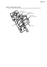
Page 6: ...ARD and the MECHANISM DECK with the extension cable and inspect the MECHANISM DECK CAUTION 2 REPLACING THE CONNECTING CORD When replacing the connecting cord fix it at the position in the figure so that the copper conductor of the cord and the steel plate contact GND adequately copper conductor of the cord connecting cord ...

Page 7: ...D extension cable J 2501 199 A 25P L300 extension cable J 2501 225 A 9P L300 extension cable J 2501 243 A 17P L300 DMB07 BOARD I O BOARD Connect the I O BOARD and the DMB07 BOARD by using the three extension cables and inspect the DMB07 BOARD ...

Page 8: ...ont Panel Top Panel A DISC indicator B Touch Panel Sensor 41 C Front panel display 104 D DOLBY DIGITAL indicator E DTS indicator F DOLBY PRO LOGIC II indicator G D C S indicator Lights up when activated H 1 power switch standby indicator 39 I Disc slot 39 J Z eject 39 VOL FUNCTION ...

Page 9: ... 62 63 J DSGX 66 K DVD SETUP 34 71 85 L SUBTITLE 68 M AUDIO 60 N ANGLE 67 O Number buttons 43 43 48 53 67 69 71 74 76 P ENTER Q TUNER MENU 79 81 R TV 1 on standby 74 S 1 standby 34 39 80 T SONY TV DIRECT 76 U TUNER BAND 79 80 81 V FUNCTION 39 78 80 81 W m M SLOW TUNING 47 52 79 80 X x stop 40 42 43 69 80 Y X pause 40 Z MUTING 40 wj DVD MENU ALBUM 43 45 46 wk VOL 40 80 wl O RETURN 43 45 46 48 53 69...

Page 10: ... MECHANISM DECK CDM80AT DVBU29T Page 13 3 12 CHASSIS TOP Page 16 3 15 DRIVER BOARD Page 18 3 8 DMB07 BOARD Page 14 3 9 DISPLAY BOARD Page 14 3 5 DLED BOARD Page 12 3 10 I O BOARD Page 15 3 11 DVD POW BOARD Page 15 3 16 RF BOARD Page 19 3 18 BASE UNIT Page 20 3 13 LEVER LOADING R L Page 17 3 14 DISC STOP LEVER DISC SENSOR LEVER Page 18 3 17 OPTICAL PICK UP DBU 3 Page 19 3 19 LEVER BU LOCK Page 20 3...

Page 11: ...r rear 4 stand section 2 four claws 1 two screws HEX 4 10 3 3 COVER MAIN CDM q four screws BVTP 3 8 qa cover CDM 1 two covers SH 9 four covers SH 8 cover MAIN 2 two screws BVTP 3 8 3 two screws 6 four claws 4 six claws 5 hook 7 cover SYS ...

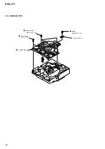
Page 12: ... DLED BOARD 4 four screws BVTP 2 6 8 1 screw BVTP 3 8 5 six screws BVTP 3 8 8 chassis section 3 side panel CDM 6 four dowels 7 wire flat type 18core CN401 2 screw BV3 3 CR 1 hook 3 two dowels 2 indicator DISC 5 DLED board 4 connector 3p ...

Page 13: ...eon assy 1 two screws BVTP 2 6 8 4 two screws BVTP 2 6 8 8 two screws BVTP 2 6 8 7 bracket escutcheon 3 connector 2p 2 connector 4p 9 STBY KEY board q EJECT KEY board 5 two dowels 6 two hooks 1 four screws BVTP 3 8 2 wire flat type 29core 3 connector 7p CN701 4 mechanism deck CDM80AT DVBU29T ...

Page 14: ... 13core CN101 2 wire flat type 17core CN105 4 wire flat type 25core CN107 5 wire flat type 29core CN501 6 connector 13p CN102 9 connector 2p CN402 8 connector 2p CN401 q heat sink DMB 5 wire flat type 12 core CN451 6 DISPLAY board 1 three screws BVTP 3 8 3 screw BVTP 3 8 2 indicator FUNC 4 clamp L35 ...

Page 15: ...ector 12p CN203 3 connector 8p CN202 4 connector 2p CN103 9 I O board 5 connector 7p CN102 1 four screws BVTP 3 8 7 wire flat type 12 core CN303 9 wire flat type 18 core CN304 2 connector 9p CN301 8 connector 8p CN901 4 connector 4p CN902 5 connector 7p CN305 6 connector 14p CN302 1 four screws BVTP 3 8 q DVD POW board 3 connector 2p CN910 ...

Page 16: ...16 HCD LF1 3 12 CHASSIS TOP 1 screw BVTP 2 6 8 4 three screws BVTP 2 6 8 3 two screws P 2 10 5 chassis top 2 lever CL UP2 ...

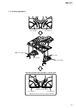
Page 17: ... R Align the horizontal position lever loading L Install the both levers so that they move symmetrically 2 two hooks 4 two hooks 3 lever loading L 5 lever loading R spr T loading L spr T loading R 1 1 PRECAUTION DURING LEVER LOADING R L INSTALLATION ...

Page 18: ...p lever so that the both holes are aligned hole 1 gear cap 3 two claws 5 two hooks 6 disc stop lever disc stop lever 4 disc sensor lever PRECAUTION DURING DISC STOP LEVER INSTALLATION 2 gear IDL L 3 Remove soldering from the two points 2 three screws BVTP 2 6 8 5 DRIVER board 4 motor pully assy 1 belt MOT ...

Page 19: ... RF BOARD 3 17 OPTICAL PICK UP DBU 3 4 RF board 2 wire flat type CN003 3 wire flat type CN001 1 claw 1 two step screws M 2 step screw M 3 two insulators RB 4 insulator 6 optical pick up DBU 3 5 tension coil spring H 1 ...

Page 20: ...3 19 LEVER BU LOCK 4 floating screw PTPWHM 2 6 5 floating screw PTPWHM 2 6 3 holder down spring 6 base unit 1 screw BVTP 2 6 8 2 lever CL UP2 5 three hooks 4 6 lever BU lock 1 gear cap 2 gear BU lock 3 floating screw PTPWHM 2 6 ...

Page 21: ...AR IDL B 1 washer 3 1 0 4 2 close lever spring 4 shaft disc stop 5 close lever 3 claw 3 gear puley 2 claw 9 DIR lever 5 gear IDL A q gear IDL B 1 DIR spring 8 stopper 6 Loosen the screw 7 Hold the release lever and change the direction 4 gear cap ...

Page 22: ...22 HCD LF1 3 22 GEAR IDL C 6 claw 1 gear IDL F 5 gear loading lever 2 two claws 4 three hooks 3 gear IDL D 7 gear IDL C ...

Page 23: ...e optical pick up to the position durable to vibration Use this mode when returning the set to the customer after repair Procedure 1 Press the 1 button to turn the set on 2 While the power is ON excluding the mode of Power ON Animation mode press the FUNCTION R button to set the function DVD 3 Remove the disc 4 Touch the Sensor on Touch Panel and press the A button simultaneously for several secon...

Page 24: ...ress the ENTER R button while the message Repeat Limit Command Out is being displayed The message Limit Off is displayed 12 DVD Service Procedure 1 Press the TEST MODE key S301 inside the product or the RETURN O R button 2 The message DVD Service is displayed 3 Press the ENTER R button while the message DVD Service is being displayed The message DVD Service On is displayed 4 Press the ENTER R butt...

Page 25: ...Revision x xx OPERATING TEST MODE 0 SYSCON DIAGNOSIS The same contents as board detail check by serial interface can be checked from the remote commander operation On the Test Mode Menu screen press 0 R key on the remote commander and the following Check Menu will be displayed Syscon Diagnosis Check Menu 0 Quit 1 All 2 Version 3 EEPROM 4 GPIO 5 SD Bus 6 Video 0 0 Quit Quit the Syscon Diagnosis and...

Page 26: ...c check memory SL 3 Wait 300 msec 4 Set disc type SL 5 LD on 6 Spindle start 7 Wait 1 sec 8 Focus servo on 0 9 Auto track offset adjust 10 CLVA on 11 Wait 500 msec 12 Tracking on 13 Wait 1 sec 14 Sled on 15 Check CLV on 16 Auto LFO adjust 17 Auto focus offset adjust 18 Auto tilt position adjust 19 Auto focus gain adjust 20 Auto focus offset adjust Drive Auto Adjustment Adjustment Menu 0 ALL 1 DVD ...

Page 27: ...fset adjust 10 CLVA on 2 DRIVE MANUAL OPERATION Note This mode is used for design and not used in service fundamentally On the Test Mode Menu screen press the 2 R key on the remote commander and the Operation Menu will be displayed For the manual operation each servo on off control and adjustment can be executed manually In using the manual operation menu take care of the following points These co...

Page 28: ...the usual trace mode becomes active In the trace mode DVD sector address or CD time code is displayed This is not displayed where the spindle is not locked The spindle could run overriding the control if the spindle system is faulty or RF is not present In such a case do not operate CLVA Servo Control 1 LD off R Sled FWD 2 Focus off L Sled REV 3 SPDL off U Sled Reset 4 CLVA off D Sled Limit 5 Trk ...

Page 29: ...ed in the EEPROM If CLV has been applied the jitter is displayed for reference for the adjustment Track Layer Jump 1 1Tj FWD 2 1Tj REV 3 500Tj Fine FWD 4 500Tj Fine REV 5 10kTj Dirc FWD 6 10kTj Dirc REV 7 20kTj Dirc FWD 8 20kTj Dirc REV 0 All Servo Off Exit RETURN Non EEPROM Write Adjust 1 Focus Offset 2 Focus Gain 3 Trk Offset Coarse 4 Trk Offset Fine 5 Trk Gain 6 EQ Boost 0 All Servo Off Exit RE...

Page 30: ...x xx xx Select 1 9 Scroll UP DOWN 1 Latest EMG Exit RETURN EEPROM Data 2 2 CDRW DVDRW Focus Gain xx xx Trk Gain xx xx Focus Offset xx xx Trk Offset xx xx EQ Boost xx xx Next UP Default CLR Exit RET 2 7 Disc Check Memory On this screen measure the mirror time of chucked disc and write to the EEPROM 2 8 Error Rate Display On this screen measure and display the error rate UC Incorrect value CR Correc...

Page 31: ... xx 2 aa bb cc xx xx xx xx xx 3 aa bb cc xx xx xx xx xx 4 aa bb cc xx xx xx xx xx 5 aa bb cc xx xx xx xx xx 6 aa bb cc xx xx xx xx xx 7 aa bb cc xx xx xx xx xx 8 aa bb cc xx xx xx xx xx Scroll UP DOWN 1 Latest Err Exit RETURN aa Initialization is completed or not FF Complete other number Not complete bb Operating status of mechanism deck at an error occurred lod sq jcp 00 Initializing 10 to 15 Ope...

Page 32: ...e servo circuit RF amplifier IC001 DSP IC509 motor driver IC501 EEPROM IC903 so on are replaced re adjusting the servo circuit is necessary Select ALL at 1 DRIVE AUTO ADJUSTMENT Refer to page 26 in TEST MODE and adjust DVD SL single layer CD and DVD DL dual layer TEST DISC LIST Use the following test disc on test mode TDV 520CSO DVD SL PART No J 2501 236 A LUV P01 CD PART No 4 999 032 01 TDV 540C ...

Page 33: ...OMPONENT VIDEO q R G B Abbreviation AUS Australian model CND Canadian model E41 Chilean and peruvian models EA Saudi Arabia model HK Hong Kong model KR Korea model MX Mexican model RU Russian model SP Singapore model TW Taiwan model For Printed Wiring Boards Note X parts extracted from the component side a Through hole f internal component Pattern from the side which enables seeing The other layer...

Page 34: ...75 13 GFS GFS_CD 71 3 MUTE MUTE_CD 59 7 SENS SENS_CD 9 76 SQSO SQSO 52 SCLK_CD 72 4 DATA DATA_CD 49 63 MD2 71 XTAI DOCTR ISBTEST 3 77 SQCK 69 XTSL CDSP2 10 85 XRD XRD 17 58 GFS_DVD GFS 107 45 109 SCK_DSD 4 XRST_2753 AEP0 64 JIT 77 SACD DVD 84 XWR XWR 18 12 XCS_DVD XCS 19 25 XRST_1882 XRST 164 22 INT0_DVD XINT0 20 23 INT1_DVD XINT1 21 SQCK 54 2 XRST XDRST 98 6 CLOK CLOK_CD 50 5 XLAT LAT_CD 27 FOK_C...

Page 35: ...47 48 50 51 53 54 56 HA1 HA3 HAD0 HAD15 ADDRESS BUS DATA ADDRESS BUS DATA ADDRESS BUS 22 19 14 11 3 2 207 206 HAD0 HAD15 HA1 HA3 HAD0 HAD15 HA1 HA2 HAD0 HAD15 HA1 HA3 HA4 HA22 12 CE WE 14 OE 1 A0 A20 195 HCS0 WEH UDS 27 HREAD ML MDI MC ML MDI MC 25 DQ0 DQ15 56 MCLK CE WE OE IC203 128Mbit SD RAM 68 CLK DQ0 DQ31 A0 A11 MA0 MA11 MD0 MD31 42 33 45 46 49 MCS0 20 CS 53 MWE 17 WE 51 MRAS 19 RAS 52 MCAS 1...

Page 36: ...1 24 27 32 20 19 D FIL INIT D FIL SELEXT 139 136 134 131 162 159 157 154 152 151 149 148 A0 A11 141 DCLK 66 DSAR 40 DSIFR 69 DSAC 41 DSICT 71 DSALFE 42 DSISW 74 DSALS 43 DSISL 76 DSARS 44 DSISR 60 BCKAO 38 DSBCK 13 EXCKO1 27 MCK 4 SELEXT 20 PLRCK 19 PBCK 17 MCKOUT 23 POFLR 22 POCSW 21 POSLR AV0 AV7 K L 164 115 XSRQ XSRQ H 11 MCKI 768FS E J N D A TESTI ISBTEST XRST_DSD DATA1 DATA3 DATA2 LRCK ZIVA B...

Page 37: ...P SECTION S CB R Y G C CUBS TO SA WSLF1 SYSTEM CONNECTOR FLG401 FLUORESCENT INDICATOR TUBE VF1 28 29 D464 VF2 32 33 16 FL DATA 17 FL CLK 14 FL LAT 15 FL BK 11 LED 0 Q464 LED DRIVER Q003 Q005 SWITCH Q306 Q901 REG CONT INVERTER 12V D C S D463 12 LED 1 Q463 LED DRIVER PRO LOGIC D462 18 LED 2 Q462 LED DRIVER DTS D461 19 LED 3 Q461 LED DRIVER DIGITAL D472 20 LED 4 Q472 LED DRIVER DISC D471 22 STBY LED ...

Page 38: ...C003 R022 R023 R013 R011 R017 R015 R026 R027 R028 R029 R031 R 0 2 4 R 0 2 5 R 0 3 5 R 0 2 0 R 0 1 9 R041 L002 L001 D002 D001 R006 R010 R001 R021 R016 R014 R012 R018 CN001 CN003 R033 R046 R047 R034 R 0 9 1 Q001 Q002 R009 R008 R007 R005 R004 R003 SIDE A RF BOARD SIDE B RF BOARD IC001 IC003 DMB07 BOARD CN501 Page 41 A E E OPTICAL PICK UP BLOCK DBU 3 1 684 822 12 12 1 684 822 12 12 1 16 17 32 48 33 64...

Page 39: ...006 R029 R028 R027 JL002 JL001 C032 C034 C049 C009 C035 CN003 CN001 CN002 C025 C006 C013 R005 R009 R035 R019 R020 C041 R001 Q001 Q002 C008 R041 JL004 C030 C026 1000p R091 560k 0 5 R033 100k C050 0 0033 C052 0 1 R046 10k R047 33k 0 47 C051 0 47 470 0 033 0 033 680p 0 1 0 100 6 3V 470 33 33 10 16V 1SS355TE 17 470 100 6 3V 1000p 33 33 10 16V 1SS355TE 17 220 100 820 2200p 2200p 2200p 0 0 0 0 0 0 0 0 1...

Page 40: ...7 for IC Block Diagram IC701 B DVD POW BOARD CN305 Page 53 M701 LOADING TRIGGER DISC IN OUT CHUKING 1 9 M 1 2 A B C 3 4 D701 R702 R701 C705 C711 S702 S703 S701 CN701 No mark DVD STOP 7V B DVD POW BOARD 1 2 CN305 Page 54 IC B D IC701 CN701 R702 R701 C711 C705 D701 S703 S701 S702 M701 BA6956AN 7P CT L 100 680 10 50V 0 01 MTZJ T 77 4 7C TRIGGER DISC IN OUT CHUKING LOADING ...

Page 41: ... C926 C927 R962 C592 R747 FB105 C202 R748 CN501 D901 FL501 FL502 FL901 IC503 IC509 IC901 R758 L103 R760 R504 C266 C265 C263 R506 R510 R511 R523 C261 R599 R593 C253 C252 R588 R586 R584 C925 C392 C248 R940 R942 R572 R943 R568 R567 C246 R566 R565 R564 R563 R562 CN102 R561 R560 R559 R558 C245 C242 C241 C239 R970 C227 R551 R550 C214 R545 R536 C547 R213 C283 C279 C278 C277 C291 X901 R299 R263 CN107 R936...

Page 42: ...506 C504 C503 C525 C527 IC203 C529 R742 C570 R743 C589 C513 R744 R745 C906 C908 C909 C910 C913 C918 R746 IC907 C203 FL908 IC501 IC903 R750 Q901 R699 R698 R694 R503 C272 C271 C270 C269 C268 C267 R935 C262 R512 R513 R516 R517 R519 R520 R521 R524 R525 C260 C257 C256 C255 C254 R591 R589 R587 R581 R580 R579 R573 C251 C250 C249 C247 R9980 C244 C243 R9981 C240 C238 C237 C236 C235 C234 C233 R9998 R9999 C2...

Page 43: ...1k 1k 1k 1k 1k 0 1 1k 1k 0 10 16V 0 0022 10 220p 10 0 220p 10 33k 10k 100k 0 47 100 4V 10 0 1 0 01 10 29P 0 022 0 0033 0 1 0 0015 100p 3 3k 0 1 1k 0 100p 1M 470k 10 0 01 10k CXD3068Q 1M 0 1 0 0 0 0 1 0 1 10 B1 B2 B3 B6 B8 B9 B10 B11 C2 C3 C4 C5 C7 C8 C9 C10 D1 D2 D3 D4 D5 C1 PI TE FE FE TE RFAC RFAC MIRR DATA_RF WFCK GSCOR XRST_CD DATA XLAT CLOK SENS SCLK COUT MIRR SCOR RF_AC MDP MUTE_CD C2PO LDON...

Page 44: ...k 33k 33k 0 0015 8 2k 1k NJM3404AV TE2 10 0 01 100 4V 0 1 0 0015 100k 100k 100k 10k 100k 0 01 10 10 0 01 10 0 01 10 0 01 0 01 0 01 22k 8 2k 0 047 0 47 2 2k 47k 22k 1M 0 0 0 01 0 01 0 01 0 01 0 01 0 10k 0 100p 0 100k 4V 0 0047 10 NJM3404AV TE2 0 0015 10k 0 1 8k 470k 0 01 1k 100 22 100 0 1 0 1 10k 100p 10k 33k 22 TMC57929PGF RDP B1 B2 B3 B6 B8 B9 B10 B11 E1 E2 E3 SIGNAL_BUS ANALOG_BUS WPK SD7 SDEF S...

Page 45: ...0 10k 10k 0 01 0 01 0 01 0 01 0 01 100 4V 0 01 0 01 0 01 22 22 22 22 22 22 22 0 01 0 01 0 01 0 01 0 01 22 A1 A2 D3V SAMBA_SIGNAL_BUS SAMBA_CTRL_BUS TCK TMS TRST ANALOG_BUS WPK TDI_SACD DGND RF_AC AV0 AV1 AV2 AV3 AV4 AV5 AV6 AV7 SA4 SA5 SA6 SA7 SA8 SA9 DCLK DCKE WAVRB DSBC DSFL DSFR DSSW DSSL DSSR XMSLAT MSCK MSDATI SHRRDY XRST_DSD SHRMUT DSD_MSCKI ISBTEST XSRQ_SAMBA XSHD SDEF MSDATO XDCK XSAK SA0 ...

Page 46: ... C821 R806 C847 FL814 C845 C850 C846 FL816 C825 C824 R813 R858 IC802 0 0 0 0 0 100 0 01 0 01 0 01 10k 100 0 01 100 0 01 0 01 100 4V 100 4V 0 01 0 01 0 0 A1 A2 D FIL_CTRL_BUS ZIVA_5 1CH_BUS D3V DGND DSBC DSFL DSFR DSCT DSSW DSSL DSSR D FIL_SELEXT D FIL_INIT FLR A CSW A SLR A LRCK A BCK A MCK A DATA3 DATA2 XCK1 DATA1 LRCK1 BCK1 DSMCK2 DIGITAL AUDIO PROCESSOR CXD9742Q 0 22µH DATA 0 PCM_5 1CH_BUS_A DM...

Page 47: ...k 150k 150k 10k 10k 10k 100k 100k 10k 56k 56k 22 16V 0 01 220 4V 10 100 6 3V 1SS355TE 17 0 220 4V 13P 12k 0 01 8 2k FAN8035L C2 C3 C4 C5 C7 C8 C9 C10 C1 VGND D3V DGND D5V AUDIO_DGND AUDIO_AGND AUDIO_5V V5V A3V 2 DGND D3V D3V DGND D3V MUTE_2D TFDR TRDR FFDR FRDR TSD M SP_ON SPIN FJMP2 FJMP1 SLEDA SLEDA SLEDB SLEDB SPDL SPDL TRK TRK FCS FCS DSAVE SLEDCTRL SLEDA SLEDB SLED SPFG M 12V MGND D 5V V 5V D...

Page 48: ...1G32DCKR BR24L16F WE2 33000p SM8707GV G E2 100 10k 10k SN74AHC2G74HDCUR 22 10k 22 CXP973064 245R 9P 10K D1 D2 D3 E1 D4 E2 E3 D5 ZIVA_CTRL_BUS SAMBA_CTRL_BUS D_FIL_CTRL_BUS VIDEO_SW V MUTE A0 A1 A2 A3 A4 A5 A6 A7 XINIT0 XINIT1 D0 D1 D2 D3 D4 D5 D6 D7 XCS1882 XHRD XHWR CLK_RF DATA_RF SENS XLAT TXD RXD MD2 PI JIT TE FJMP1 FJMP2 SLEDA SLEDB LOCK FOK SCLK GFS_CD SP_ON SPFG SLED MUTE_2D MUTE_CD GFS_DVD ...

Page 49: ...APWR SN74LV573APWR 0 01 0 01 0 01 0 01 4 7k 4 7k 0 0 0 47k DTC114TE TL F3 F4 F5 F6 ZIVA_CTRL_BUS SIGNAL_BUS SAMBA_SIGNAL_BUS D3V SD7 SD6 SD5 SD4 SD3 SD2 SD1 SD0 XSAK SDEF XDCK XSHD AV7 AV6 AV5 AV4 AV3 AV2 AV1 AV0 XSAK SDEF XSHD XSRQ XSRQ_SAMBA XDCK XSRQ_ZIVA SACD DVD A B Y GND VCC ST SL Y 7 10 LATCH INVERTER LATCH LEVEL SHIFT LATCH R9982 R9983 0 R9985 0 0 R9984 0 Page 50 Page 45 Page 44 Page 48 Pa...

Page 50: ...01 17P 1 0 33 0 0 100 100 0 R219 0 0 100 100 0 01 0 01 0 01 0 01 100p 1SS355TE 17 ZIVA5X C1F 4 7k 0 01 0 01 0 01 0 01 0 01 100 1k 1k 0 01 820 0 10k 75 75 75 75 75 F4 G2 G3 G4 G5 G6 G7 G8 G9 F3 F6 F5 A3V 2 DGND D5V D3V VGND V5V ZIVA_5 1CH_BUS TRST TDI_SACD TMS TCK MWE DRVCLK DRVTX DRVRX DRVRDY DRVIRQ RST_SPC MCLK I2C_SIO I2C_SCL CN202 4P RXD TXD GND D5V FOR CHECK 1 2 3 4 MDQM0 MDQM1 SYS_RST CS_SPC ...

Page 51: ...HAD0 HAD1 HAD2 HAD3 HAD4 HAD5 HAD6 HAD7 HAD8 HAD9 HAD10 HAD11 HAD12 HAD13 HAD14 HAD15 HA1 HA2 HA3 HA4 HA5 HA6 HA7 HA8 HA9 HA10 HA11 HA12 HA13 HA14 HA15 HA16 HA17 HA18 HA19 HA20 MA11 HA21 MD0 MD1 MD2 MD3 MD4 MD5 MD6 MD7 MD8 MD9 MD10 MD11 MD12 MD13 MD14 MD15 MD16 MD17 MD18 MD19 MD20 MD21 MD22 MD23 MD24 MD25 MD26 MD27 MD28 MD29 MD30 MD31 HAD0 HAD1 HAD2 HAD3 HAD4 HAD5 HAD6 HAD7 HA11 HA10 HA9 HA8 HA7 H...

Page 52: ... 10W 220 1 10W 220 1 10W 220 1 10W 100 6 3V 220 1 10W 0 01 0 01 0 01 0 01 0 01 0 01 100p 100p 0 1 0 1 0 1 0UH 0 01 PCM1609KPTR D A CONVERTER 3 3V REGULATOR 220 1 10W 0 01 10 1 10W 1SS355TE 1 7 1SS355TE 1 7 1SS355TE 1 7 22 1 10W 1SS355TE 17 1SS355TE 17 0 1 0 DAC_CTRL_BUS DGND D3V AUDIO_5V AUDIO_AGND AUDIO_DGND PCM_5 1CH_BUS A MDI MC ML DMX A MCK A FLR A SLR A CSW A BCK A LRCK A CN107 25P BA33BC0FP ...

Page 53: ...44 FB345 FB337 FB335 FB339 FB352 FB354 FB356 FB348 FB360 FB314 FB317 FB319 FB321 FB323 D931 R379 R380 R381 R378 C300 D302 D303 D301 R351 D313 D311 D315 FB305 FB306 FB307 FB308 FB309 FB310 FB311 FB312 FB329 FB324 R307 R306 R308 FB325 FB326 FB327 FB328 FB330 FB331 FB332 FB333 R313 R314 R311 R312 R309 R310 R315 R316 R337 R336 R327 R328 R329 R382 R383 R384 R366 R367 R374 R375 R305 R303 R390 R391 R398 ...

Page 54: ...9 D315 IC302 D316 R376 R395 CN303 CN300 CN304 C318 R331 R329 R330 R328 R327 CN305 R336 R300 C310 R346 CN301 CN302 R322 R325 R317 R335 R316 R315 R314 R313 R312 R311 R310 R309 R308 R307 R306 R304 S301 IC303 IC301 EPT301 X301 10k 2SC2712 47k 47k 0 22 MUN2211T1 100 100 100 0 0 0 0 0 MMDL914T1 0 0 0 0 0 0 0 0 0 0 3 3k 100 16V 100 16V 0 XX 100 100 100 100 100 100 2SC2712 2SC2712 470k 47k 0 1 0 01 B 3 3k...

Page 55: ...0JF MUN2213 100 11EQS04 MUN2213 SI 8033S 100 16V 1000 16V 100 16V 0 2012 0 0 0 001 50V B 1000 16V 22 10V 100 6 3V 0 1 2012 B 0 1 2012 B 10EDB40 0 1 2012 B 1000 16V 0 001 50V B 1000 16V 0 1 2012 B 1000 16V 180 2012 0 001 50V B 1000 16V 1000 16V 100 6 3V 0 1 2012 B 0 1 2012 B 0 1 2012 B 2 4k 2012 100 16V 3 3k 2012 10EDB40 0 1 2012 B 22 10V 0 1 B 3225 4PIN PH 11EQS04 180 560 11EQS04 8PIN PH L 2P PH L...

Page 56: ...G401 C457 C456 C458 C459 C455 C469 C451 R465 R466 R467 R468 R469 R460 R459 R458 R457 R456 R455 R452 R454 R453 R451 C460 C461 C454 D455 FB460 FB451 FB452 FB453 FB454 FB455 FB456 FB457 FB458 FB459 L452 L451 T451 Q451 Q452 C452 Q461 1 2 A B C D 3 4 5 6 7 8 9 10 11 12 53 Semiconductor Location Ref No Location D451 B 2 D452 B 2 D453 B 2 D454 B 2 D455 B 10 D461 B 6 D462 B 6 D463 C 6 D464 D 6 Q451 B 11 Q...

Page 57: ...R457 R456 R455 R459 R453 R454 T451 FB451 FB452 FB453 FB454 FB455 FB456 FB457 FB458 FB459 FB460 2SD1624 T TD 2SD1624 T TD 1 0k 2012 MMDL914T1 MMDL914T1 MMDL914T1 MMDL914T1 10k 2012 NSCW100 330 0 NSCW100 330 NSCW100 330 NSCW100 330 MUN2213T1 MUN2213T1 MUN2213T1 MUN2213T1 47k 47k 47k 0 2012 0 033 200V 47 16V 0 1 100V B 47 63V MM3Z6V2ST1 0 1 B 100p CH 100p CH 100p CH 12PIN FFC S 1MM 0 1 B 0 1 B 0 1 B ...

Page 58: ...R425 R426 C413 C410 C411 R408 C403 C402 R405 R 4 1 3 R 4 1 0 R 4 1 1 R 4 1 2 R 4 2 2 R 4 2 1 R 4 2 0 R 4 2 3 C 4 1 4 C 4 1 5 C 4 1 6 C 4 0 5 R 4 0 9 C 4 0 7 C 4 0 6 J W 4 0 2 R 4 0 2 X 4 0 1 R 4 4 1 R 4 4 0 R 4 3 9 R 4 3 7 R 4 3 5 R 4 0 1 R 4 0 6 R 4 0 4 R 4 3 3 R 4 3 2 R 4 3 1 R 4 0 7 R 4 3 6 R 4 3 8 C412 CN401 L 4 0 1 CN402 C 4 0 4 CN310 S402 R471 C471 CN311 D471 S 4 0 1 C N 3 0 9 R472 C472 Q 4 ...

Page 59: ...N311 C471 CN309 CN310 CN402 CN401 R407 R402 R401 R408 C402 C412 C411 R421 R422 CL400 CL401 CL402 CL403 CL404 CL405 CL406 CL410 CL411 CL412 CL413 CL414 CL415 CL416 X401 IC402 2 2k 2 2k 2 2k 2 2k 4 7k 4 7k 4 7k 4 7k 4 7k 4 7k 2 2k 4 7k 100 100 10k 10k 10k EJECT STANDBY NSCW100 MUN2211T1 0 1 B 0 1 3225 100 6 3V 10 16V 330 QT1100 1 10V B 1 10V B 10k 0 1 B 100 0 3216 100 100 100 100 100 1k 0 068 0 068 ...

Page 60: ...R 2 0 5 D 9 0 2 D 9 0 1 F B 2 0 1 F B 2 0 2 F B 2 0 3 F B 2 0 4 Q 0 0 4 Q 0 0 5 Q 0 0 3 R 0 6 6 R 0 6 7 R 1 7 6 R 1 2 6 R 1 6 6 R 1 1 6 R 1 5 6 R 1 0 6 R 1 0 7 R 1 0 8 R 1 1 7 R 1 6 7 R 1 2 7 R 1 7 7 R 1 5 7 R 1 5 8 F B 1 0 1 J W 1 0 5 J W 1 0 2 J W 1 0 1 J W 1 0 3 D 1 0 1 D 1 0 2 C N 1 0 1 R 1 7 1 R 1 7 2 R 1 7 3 R 1 7 5 R 1 2 1 R 1 2 2 R 1 2 3 R 1 2 5 R 1 6 1 R 1 6 2 R 1 6 3 R 1 6 5 R 1 1 1 R 1 ...

Page 61: ...N203 R208 R207 R206 R205 R204 C212 C211 C210 C215 C216 C217 C218 JW203 R202 R210 C001 C106 IC901 IC902 C146 C145 C148 C147 C150 C149 C156 C107 JW106 R108 R158 C203 10 16V 10 16V 10 16V 10 16V 100 16V 10 16V 10 16V 100 16V 10 16V 10 16V 10 16V 10 16V 10 16V 10 16V 10 16V 10 16V 10 16V 1 50V 1 50V 1 50V 100 6 3V 100 16V 0 0 0 0 0 0UH MM1623BFBE DTC124EKA T146 4 7k 4 7k 100k 4 7k 4 7k 100k 4 7k 4 7k ...

Page 62: ... ns 5 6 Vp p 1 V DIV 10 ns DIV 0 IC901 r XTAL 50 ns 3 8 Vp p 1 V DIV 20 ns DIV qa IC207 zcz VDAC_0 H 1 5 Vp p 500 mV DIV 20 µs DIV qs IC207 zx VDAC_1 H 1 2 Vp p 500 mV DIV 20 µs DIV qd IC207 zxb VDAC_2 AEP UK RU H 1 1 Vp p 500 mV DIV 20 µs DIV qd IC207 zxb VDAC_2 EXCEPT AEP UK RU H 1 3 Vp p 500 mV DIV 20 µs DIV qf IC207 zxx VDAC_3 AEP UK RU H 1 1 Vp p 500 mV DIV 20 µs DIV qf IC207 zxx VDAC_3 EXCEP...

Page 63: ...41 48 47 46 45 GCA OFFSET CANSEL 5 FROM S PORT GCA 40 GCA OFFSET CANSEL 6 FROM S PORT 3 FROM S PORT GCA GCA CEFDB CP CN LOW IMPEDANCE CD DVD SUB GCA MUX GCA LPF GCA LPF 39 38 37 36 OFFSET CANSEL PEAK BOTTOM HOLD BOTTOM ENVELOPE INPUT BUFFER 5 FROM S PORT GCA LPF V25 2 TE RST 35 34 33 FOR SERVO OUTPUT PH TOP HOLD GCA SEL LINKEN MUX HOLDEN COMPA RATOR INTERNAL FDGHG HYSTERESISTER OFFSET FROM S PORT ...

Page 64: ...19 20 21 22 23 24 25 26 27 28 29 30 31 32 33 34 35 36 37 38 39 40 80 79 78 77 76 75 74 73 72 71 70 69 68 67 66 65 64 63 62 61 OPERATIONAL AMPLIFIER ANALOG SWITCH A D CONVERTER FOCUS PWM GENERATOR TRACKING PWM GENERATOR SLED PWM GENERATOR FOCUS SERVO DSP TRACKING SERVO DSP SLED SERVO DSP ASYMMETRY CORRECTOR DIGITAL PLL CLOCK GENERATOR 60 NC A9 A8 A7 A6 A5 A4 VSS NC NC A0 A1 A2 A3 VDD VDD DQ1 DQ2 DQ...

Page 65: ...PUT BUFFERS INPUT BUFFERS SENSE AMPLIFIER COLUMN DECODERS MEMORY CELLS WORD DRIVERS ROW DECODERS COLUMN ADDRESS BUFFERS UDQM 35 CLK 34 CKE 33 NC 37 NC 38 41 I O CONTROLLER PROGRAMING REGISTER 16 WE 15 17 CS 18 LDQM 14 ROW ADDRESS BUFFERS INTERNAL COLUMN ADDRESS COUNTOR LATENCY BURST CONTROLLER INTERNAL ROW ADDRESS COUNTOR TIMING REGISTER BANK CONTROLLER 8 VCC 7 WP 6 SCL 5 SDA 1 A0 2 A1 3 A2 4 GND ...

Page 66: ...27 TEST3 TOUT2 10 26 TOUT1 VDDL 11 VSS 12 25 FIR FILTER DOWN SAMPLING UNIT CLOCK GENERATOR TIMING CONTROL ROM 24 bit 720 word INT EXT DATA SELECT INT EXT CLOCK SELECT PCM MUTE TEST CONTROL PCM I F 1 OE 2 1D C1 1D 19 1Q 20 VCC 3 2D C1 1D 18 2Q 4 3D C1 1D 17 3Q 5 4D C1 1D 16 4Q 6 5D C1 1D 15 5Q 7 6D C1 1D 14 6Q 8 7D C1 1D 13 7Q 9 8D 10 GND C1 1D 12 8Q 11 LE 1 VDD1 2 VSS1 3 MO1 4 MO2 5 VDD2 6 VSS2 7 ...

Page 67: ...AGND5 VCC5 AGND6 VOUT8 AGND4 VCC4 AGND3 VCC3 13 14 15 16 17 18 19 20 21 22 23 24 ML MC MDI MDO ZERO8 DATA4 ZERO7 NC VCC1 AGND1 VCC2 AGND2 36 35 34 33 32 31 30 29 28 27 26 25 200Ω 75Ω DRIVER 75Ω DRIVER 75Ω DRIVER 75Ω DRIVER 6 75MHz LPF 6 75MHz LPF 6 75MHz LPF 13 5MHz LPF 6 75MHz 6dB 6dB 6dB 6dB 6dB 6dB LPF 75Ω DRIVER 13 5MHz LPF 6 75MHz 6dB LPF 75Ω DRIVER 13 5MHz LPF 6 75MHz 6dB LPF BIAS CLAMP CLAM...

Page 68: ...ignal input terminal 29 GND Ground terminal 30 VDD Power supply terminal 1 8V 31 GND25 Ground terminal 32 VDD25 Power supply terminal 3 3V 33 to 42 MA9 to MA0 O Address signal output to the SD RAM 43 GND25 Ground terminal 44 VDD25 Power supply terminal 3 3V 45 46 MA10 MA11 O Address signal output to the SD RAM 47 48 BA1 BA0 O Bank select signal output to the SD RAM 49 MCS0 O Chip select signal out...

Page 69: ...ta latch pulse signal output terminal 116 HIRQ2 I Busy signal input from the EEPROM 117 VDAC_4B Ground terminal 118 VDAC_VDD4 Power supply terminal 3 3V 119 VDAC_4 O Component video signal output to the video amplifier 120 VDAC_3B Ground terminal 121 VDAC_VDD3 Power supply terminal 3 3V 122 VDAC_3 O Component video signal output to the video amplifier 123 VDAC_2B Ground terminal 124 VDAC_VDD2 Powe...

Page 70: ...ect signal output to the EEPROM 163 RXD1 I Serial data input terminal for check jig 164 TXD1 O Serial data output terminal for check jig 165 WRITE_CTRL O Write control signal output to the EEPROM ZIVA_E2P 166 GNDP Ground terminal 167 VDDP Power supply terminal 3 3V 168 to 171 SDDATA7 to SDDATA4 I Stream data signal input from the DVD decoder 172 GND Ground terminal 173 VDD Power supply terminal 1 ...

Page 71: ...input terminal for JTAG Not used 200 TMS I Mode selection signal input terminal for JTAG 201 TCK I Clock signal input terminal for JTAG 202 RESET I System reset signal input from the system controller L reset 203 BUS CLK O Not used 204 GND Ground terminal 205 VDD Power supply terminal 1 8V 206 HA3 O Address signal output to the programmable ROM 207 HA2 O Address signal output to the programmable R...

Page 72: ...ystem processor and DSD decoder 27 HDB6 O Stream data signal output to the DVD system processor and DSD decoder 28 VDDS Power supply terminal 5V 29 HDB9 O Not used 30 HDB5 O Stream data signal output to the DVD system processor and DSD decoder 31 HDBA O Not used 32 HDB4 O Stream data signal output to the DVD system processor and DSD decoder 33 VSS Ground terminal 34 HDBB O Not used 35 HDB3 O Strea...

Page 73: ...dress signal output to the D RAM 90 VSS Ground terminal 91 MA9 O Address signal output to the D RAM 92 MNT1 O EEPROM ready signal output to the mechanism controller 93 MNT2 O Not used 94 XOE O Output enable signal output to the D RAM 95 XCAS O Column address strobe signal output to the D RAM 96 97 MDB8 MDB9 I O Two way data bus with the D RAM 98 VSS Ground terminal 99 MDBA I O Two way data bus wit...

Page 74: ...minal of internal CLV circuit 143 VDD Power supply terminal 3 3V 144 MDPOUT O Phase error output of internal CLV circuit 145 DFCT I Defect signal input from the DSP 146 GSCOR I Guard subcode sync S0 S1 detection signal input from the DSP 147 EXCK O Subcode serial data reading clock signal output to the DSP 148 SBIN I Subcode serial data input from the DSP 149 VSS Ground terminal 150 SCOR I Subcode...

Page 75: ...scription 169 XTA2 O System clock 33 8688 MHz output terminal 170 XTA1 I System clock 33 8688 MHz input from the clock generator 171 VDD Power supply terminal 3 3V 172 to 176 D0 to D4 I O Two way data bus with the mechanism controller ...

Page 76: ...t terminal for JTAG 28 VSCA1 Ground terminal for core 29 TDO O Data output terminal for JTAG Not used 30 TMS I Mode selection signal input terminal for JTAG 31 TRST I Reset signal input terminal for JTAG 32 to 34 TEST1 to TEST3 I Input terminal for the test normally fixed at L 35 VDCA1 Power supply terminal 2 5V for core 36 UBIT O Monitor terminal relative to DST Not used 37 XBIT O Monitor termina...

Page 77: ...l 3 3V For DSD data output 78 79 IOUT0 IOUT1 I O Two way data bus terminal Not used 80 VSCB0 Ground terminal for core 81 82 IOUT2 IOUT3 I O Two way data bus terminal Not used 83 VDCB0 Power supply terminal 2 5V for core 84 85 IOUT4 IOUT5 I O Two way data bus terminal Not used 86 VSIOB0 Ground terminal for I O 87 IANCO O Transmission information data output terminal Not used 88 IFULL I Data transmi...

Page 78: ...l output to the D RAM 143 XWE O Write enable signal output to the D RAM 144 XCAS O Column address strobe signal output to the D RAM 145 XRAS O Row address strobe signal output to the D RAM 146 VDIOA3 Power supply terminal 3 3V for I O 147 NC O Not used 148 149 A11 A10 O Address signal output to the D RAM 150 VSCA3 Ground terminal for core 151 152 A9 A8 O Address signal output to the D RAM 153 VDCA...

Page 79: ...nal output to the CD DVD SACD RF amplifier 29 MIRR I Mirror signal input from the CD DVD SACD RF amplifier and DSP 30 COUT_CD I Numbers of track counted signal input from the DSP 31 INLIM I Detection signal input from limit in switch The optical pick up is inner position when H 32 CS_ZIVA O Chip select signal output terminal 33 SI_ZIVA I Serial data input from the DVD system processor 34 SO_ZIVA O...

Page 80: ...gnal output to the DSP 73 TSD M O Thermal shut down signal output to the motor coil driver 74 FOK_CD I Focus OK signal input from the DSP 75 LOCK_CD I GFS is sampled by 460 Hz H input when GFS is H 76 LDSEL O Laser diode selection signal output terminal 77 SACD DVD O SACD DVD selection signal output terminal L DVD L SACD 78 I2C_SIO I O Two way I2C data bus with the DVD system processor and system ...

Page 81: ...dicator Tube 17 FL CLK O Fl clk data output to Fluorescent Indicator Tube 18 LED2 O LED2 drive signal output 19 LED3 O LED3 drive signal output 20 LED4 O LED4 drive signal output 21 IC VPP Not used 22 STBY LED O Standby LED drive signal output 23 NC Not used 24 NC Not used 25 NC Not used 26 DF INIT O Df init signal output to Digital Audio Proccer 27 DF SEL O Df sel signal output to Digital Audio P...

Page 82: ...Not used 67 NC Not used 68 NC Not used 69 CDM CHK SW I Chucking detection switch signal input 70 CDM OUT SW I Trigger detection switch signal input 71 CDM TRD SW I Loading out detection switch signal input 72 CDM FIN O Motor drive signal output 73 CDM RIN O Motor drive signal output 74 AVDD Power Supply 5V 75 AVSS Ground terminal 76 AVREF I Reference voltage input terminal 77 D POW SENS O Not used...

Page 83: ...in No Pin Name I O Description 95 V SW O Mute signal output to the Video Amp 96 V MUTE O RCS signal output to the Video Amp 98 NC Not used 98 NC Not used 99 AMPMCOM Not used 100 UCOM DI Ucom data input to Subwoofer ...

Page 84: ...xican model RU Russian model SP Singapore model TW Taiwan model Ref No Part No Description Remark 7 1 STAND SECTION Ref No Part No Description Remark The components identified by mark 0 or dotted line with mark 0 are critical for safety Replace only with part number specified Les composants identifiés par une marque 0 sont critiques pour la sécurité Ne les remplacer que par une pièce portant le nu...

Page 85: ... BOARD COMPLETE 65 2 148 307 01 COVER SH 66 2 108 338 01 PANEL CDM SIDE 67 2 102 732 01 PANEL CDM BACK AEP UK 67 2 102 732 11 PANEL CDM BACK US CND 67 2 102 732 31 PANEL CDM BACK HK SP 67 2 102 732 41 PANEL CDM BACK RU 67 2 102 732 51 PANEL CDM BACK EA 67 2 102 732 71 PANEL CDM BACK MX 67 2 102 732 81 PANEL CDM BACK TW 68 2 102 733 31 PANEL MAIN BACK US CND 68 2 102 733 41 PANEL MAIN BACK EXCEPT U...

Page 86: ...No Part No Description Remark 108 A 1065 870 A DVD POW BOARD COMPLETE SP HK KR TW 108 A 1073 690 A DVD POW BOARD COMPLETE RU 108 A 1082 495 A DVD POW BOARD COMPLETE EA 108 A 1082 558 A DVD POW BOARD COMPLETE MX E41 108 A 1105 773 A DVD POW BOARD COMPLETE AUS 109 1 829 822 11 WIRE FLAT TYPE 18 CORE 110 A 1065 359 A DISPLAY BOARD COMPLETE 111 1 829 823 11 WIRE FLAT TYPE 12 CORE 112 2 102 742 01 INDI...

Page 87: ...G 402 4 248 723 01 SPR E HOLDER DOWN 403 4 245 653 01 BELT MOT 404 4 245 662 01 PULLEY GEAR 405 4 245 646 01 GEAR IDL F 406 4 245 644 01 GEAR IDL D 407 4 245 645 01 GEAR IDL E 408 4 246 203 01 LEVER RELEASE 409 4 245 630 01 LEVER SW 410 4 951 620 01 SCREW 2 6X8 BVTP 411 4 245 639 01 LEVER CL UP2 412 1 688 337 11 DRIVER BOARD M701 X 2021 530 1 MOTOR PULLEY ASSY LOADING 9 7 685 106 19 SCREW P 2X10 T...

Page 88: ... 648 01 GEAR IDL H 457 4 245 655 01 CHASSIS TOP 458 4 245 631 01 SPT T LOADING R 459 4 245 650 01 GEAR IDL J 460 4 245 651 01 GEAR IDL L 461 4 245 640 01 GEAR CAP 462 4 245 626 01 CAP CLAMPER DBU 1 463 4 245 638 01 LEVER CL UP1 464 4 985 672 01 SCREW PTPWHM2 6 FLOATING 465 4 245 636 01 SPR T CL DOWN 466 4 245 658 01 LEVER DISC STOP 467 4 245 659 01 LEVER DISC SENSOR 468 4 245 632 01 SPR T LOADING ...

Page 89: ...B 505 4 245 814 01 LEVER DIR FIRST 506 4 245 633 01 SPR E DIR BACK 507 4 245 660 01 LEVER DIR 508 4 245 641 01 GEAR IDL A 509 4 245 640 01 GEAR CAP 510 4 245 628 01 LEVER BU LOCK 511 4 248 206 01 WASHER 3 1 0 4 512 4 245 624 01 LEVER CLOSE 513 4 245 635 01 SPR E LEVER CLOSE 514 4 245 629 01 GEAR BU LOCK 515 4 245 644 01 GEAR IDL D 516 4 985 672 01 SCREW PTPWHM2 6 FLOATING Ref No Part No Descriptio...

Page 90: ... DBU 3 606 X 2021 529 1 HOLDER BU ASSY 607 3 053 847 41 INSULATOR 608 2 102 418 01 SPRING H 1 TENSION COIL Ref No Part No Description Remark Ref No Part No Description Remark The components identified by mark 0 or dotted line with mark 0 are critical for safety Replace only with part number specified Les composants identifiés par une marque 0 sont critiques pour la sécurité Ne les remplacer que pa...

Page 91: ...1 CERAMIC CHIP 0 1uF 10 100V C465 1 107 826 11 CERAMIC CHIP 0 1uF 10 16V C466 1 107 826 11 CERAMIC CHIP 0 1uF 10 16V C467 1 107 826 11 CERAMIC CHIP 0 1uF 10 16V C468 1 107 826 11 CERAMIC CHIP 0 1uF 10 16V C469 1 126 514 11 ELECT 22uF 20 16V CONNECTOR CN451 1 784 371 21 CONNECTOR FFC FPC 12P DIODE D451 8 719 081 97 DIODE MMDL914T1 D452 8 719 081 97 DIODE MMDL914T1 D453 8 719 081 97 DIODE MMDL914T1 ...

Page 92: ...F 10 16V C245 1 164 943 11 CERAMIC CHIP 0 01uF 10 16V C246 1 164 943 11 CERAMIC CHIP 0 01uF 10 16V C247 1 164 943 11 CERAMIC CHIP 0 01uF 10 16V C248 1 164 943 11 CERAMIC CHIP 0 01uF 10 16V C249 1 164 943 11 CERAMIC CHIP 0 01uF 10 16V C250 1 164 943 11 CERAMIC CHIP 0 01uF 10 16V C251 1 164 943 11 CERAMIC CHIP 0 01uF 10 16V C252 1 164 943 11 CERAMIC CHIP 0 01uF 10 16V C253 1 164 943 11 CERAMIC CHIP ...

Page 93: ...20 4V C559 1 125 777 11 CERAMIC CHIP 0 1uF 10 10V C560 1 164 938 11 CERAMIC CHIP 0 0015uF 10 50V C561 1 107 820 11 CERAMIC CHIP 0 1uF 16V C563 1 164 874 11 CERAMIC CHIP 100PF 5 50V C565 1 125 777 11 CERAMIC CHIP 0 1uF 10 10V C567 1 164 943 11 CERAMIC CHIP 0 01uF 10 16V C568 1 117 370 11 CERAMIC CHIP 10uF 10V C569 1 107 820 11 CERAMIC CHIP 0 1uF 16V C570 1 117 370 11 CERAMIC CHIP 10uF 10V C573 1 16...

Page 94: ... 20 4V C860 1 164 943 11 CERAMIC CHIP 0 01uF 10 16V C861 1 164 943 11 CERAMIC CHIP 0 01uF 10 16V C863 1 218 990 11 SHORT CHIP 0 C865 1 164 943 11 CERAMIC CHIP 0 01uF 10 16V C866 1 164 943 11 CERAMIC CHIP 0 01uF 10 16V C867 1 164 943 11 CERAMIC CHIP 0 01uF 10 16V C870 1 127 772 81 CERAMIC CHIP 33000PF 10 10V C871 1 164 943 11 CERAMIC CHIP 0 01uF 10 16V C895 1 117 370 11 CERAMIC CHIP 10uF 10V C896 1...

Page 95: ... G E2 IC907 8 759 583 47 IC uPC2933T E2 JUMPER RESISTOR JW392 1 216 864 11 SHORT CHIP 0 COIL RESISTOR L103 1 216 296 11 SHORT CHIP 0 L501 1 216 296 11 SHORT CHIP 0 L704 1 412 031 11 INDUCTOR 47uH L824 1 410 985 42 INDUCTOR 0 22uH L901 1 412 031 11 INDUCTOR 47uH TRANSISTOR Q201 8 729 929 26 TRANSISTOR DTC114TE Q202 8 729 929 26 TRANSISTOR DTC114TE Q901 8 729 929 26 TRANSISTOR DTC114TE RESISTOR R10 ...

Page 96: ... 833 11 METAL CHIP 10K 5 1 10W R524 1 216 833 11 METAL CHIP 10K 5 1 10W R525 1 216 833 11 METAL CHIP 10K 5 1 10W R527 1 216 825 11 METAL CHIP 2 2K 5 1 10W R529 1 216 839 11 METAL CHIP 33K 5 1 10W R530 1 216 842 11 METAL CHIP 56K 5 1 10W R533 1 216 839 11 METAL CHIP 33K 5 1 10W R534 1 216 842 11 METAL CHIP 56K 5 1 10W R536 1 216 833 11 METAL CHIP 10K 5 1 10W R537 1 216 843 11 METAL CHIP 68K 5 1 10W...

Page 97: ... 216 801 11 METAL CHIP 22 5 1 10W R824 1 216 025 11 RES CHIP 100 5 1 10W R825 1 216 295 91 SHORT CHIP 0 R826 1 216 801 11 METAL CHIP 22 5 1 10W R827 1 216 809 11 METAL CHIP 100 5 1 10W R828 1 216 829 11 METAL CHIP 4 7K 5 1 10W R829 1 216 809 11 METAL CHIP 100 5 1 10W R830 1 216 829 11 METAL CHIP 4 7K 5 1 10W R831 1 216 839 11 METAL CHIP 33K 5 1 10W R832 1 216 864 11 SHORT CHIP 0 R839 1 216 829 11 ...

Page 98: ...5 831 A DVD POW BOARD COMPLETE US CND A 1065 870 A DVD POW BOARD COMPLETE SP HK KR TW A 1073 690 A DVD POW BOARD COMPLETE RU A 1082 495 A DVD POW BOARD COMPLETE EA A 1082 558 A DVD POW BOARD COMPLETE MX E41 A 1105 773 A DVD POW BOARD COMPLETE AUS 7 685 646 79 SCREW BVTP 3X8 TYPE2 IT 3 CAPACITOR C300 1 104 905 11 CAPACITOR 0 22F 5 5V C301 1 117 681 11 ELECT CHIP 100uF 20 16V C302 1 117 681 11 ELECT...

Page 99: ...HORT CHIP 0 FB312 1 216 864 11 SHORT CHIP 0 FB313 1 216 864 11 SHORT CHIP 0 FB314 1 216 864 11 SHORT CHIP 0 FB315 1 216 864 11 SHORT CHIP 0 FB316 1 216 864 11 SHORT CHIP 0 FB317 1 216 864 11 SHORT CHIP 0 FB318 1 216 864 11 SHORT CHIP 0 FB319 1 216 864 11 SHORT CHIP 0 FB320 1 216 864 11 SHORT CHIP 0 FB321 1 216 864 11 SHORT CHIP 0 FB322 1 216 864 11 SHORT CHIP 0 FB323 1 216 864 11 SHORT CHIP 0 FB32...

Page 100: ... CHIP 10K 5 1 10W R338 1 216 809 11 METAL CHIP 100 5 1 10W R339 1 216 809 11 METAL CHIP 100 5 1 10W R340 1 216 809 11 METAL CHIP 100 5 1 10W R341 1 216 821 11 METAL CHIP 1K 5 1 10W R342 1 216 833 11 METAL CHIP 10K 5 1 10W R343 1 216 833 11 METAL CHIP 10K 5 1 10W R344 1 216 833 11 METAL CHIP 10K 5 1 10W R346 1 216 864 11 SHORT CHIP 0 R347 1 216 809 11 METAL CHIP 100 5 1 10W R348 1 216 809 11 METAL ...

Page 101: ...MISTOR A 1065 367 A I O BOARD COMPLETE AEP UK RU A 1065 833 A I O BOARD COMPLETE EXCEPT AEP UK RU CAPACITOR C001 1 107 826 11 CERAMIC CHIP 0 1uF 10 16V C101 1 124 779 00 ELECT CHIP 10uF 20 16V C102 1 162 953 11 CERAMIC CHIP 100PF 5 50V C103 1 162 957 11 CERAMIC CHIP 220PF 5 50V C104 1 124 779 00 ELECT CHIP 10uF 20 16V C105 1 107 726 91 CERAMIC CHIP 0 01uF 10 16V C106 1 117 681 11 ELECT CHIP 100uF ...

Page 102: ...5TE 17 D902 8 719 988 61 DIODE 1SS355TE 17 D941 8 719 053 18 DIODE 1SR154 400TE 25 RESISTOR FB101 1 216 864 11 SHORT CHIP 0 FB201 1 216 864 11 SHORT CHIP 0 FB202 1 216 864 11 SHORT CHIP 0 FB203 1 216 864 11 SHORT CHIP 0 FB204 1 216 864 11 SHORT CHIP 0 FILTER FL201 1 234 177 21 FILTER CHIP EMI IC IC101 8 759 572 38 IC NJM2140R IC102 8 759 572 38 IC NJM2140R IC103 8 759 572 38 IC NJM2140R IC201 6 70...

Page 103: ...017 1 162 966 11 CERAMIC CHIP 0 0022uF 10 50V C018 1 164 172 11 CERAMIC CHIP 0 0056uF 10 25V C019 1 164 172 11 CERAMIC CHIP 0 0056uF 10 25V C020 1 162 919 11 CERAMIC CHIP 22PF 5 50V C021 1 162 919 11 CERAMIC CHIP 22PF 5 50V C022 1 162 919 11 CERAMIC CHIP 22PF 5 50V C023 1 162 919 11 CERAMIC CHIP 22PF 5 50V C024 1 162 970 11 CERAMIC CHIP 0 01uF 10 25V C025 1 107 826 11 CERAMIC CHIP 0 1uF 10 16V C02...

Page 104: ...10 563 11 CERAMIC CHIP 0 068uF 10 16V C412 1 107 826 11 CERAMIC CHIP 0 1uF 10 16V C413 1 165 176 11 CERAMIC CHIP 0 047uF 10 16V C414 1 165 176 11 CERAMIC CHIP 0 047uF 10 16V C415 1 110 563 11 CERAMIC CHIP 0 068uF 10 16V C416 1 110 563 11 CERAMIC CHIP 0 068uF 10 16V CONNECTOR CN401 1 793 990 11 FFC CONNECTOR FPC LIF NON ZIF 18P CN402 1 779 806 21 CONNECTOR 8P IC IC401 6 706 759 01 IC QT1100 IC402 6...

Page 105: ...6 A 1066 311 A STAND ASSY EXCEPT KR 6 A 1092 692 A STAND ASSY KR 60 X 2022 359 1 ESCUTCHEON ASSY 102 1 829 825 11 WIRE FLAT TYPE 17 CORE 103 1 829 824 11 WIRE FLAT TYPE 9 CORE 104 1 829 826 11 WIRE FLAT TYPE 25 CORE 106 1 829 827 11 WIRE FLAT TYPE 29 CORE 107 1 829 383 11 CABLE SYSTEM EXCEPT US CND 107 1 830 201 11 CABLE FOR SYSTEM U CA US CND 109 1 829 822 11 WIRE FLAT TYPE 18 CORE 111 1 829 823 ...

Page 106: ...ing the version at the upper right on the revised page allows you to jump to the next revised page Ver Date Description of Revision 1 0 2004 08 New 1 1 2004 10 Addition of special jig J 2501 272 A for checking RF signal waveform SPM 04109 1 2 2006 09 Addition of Australian model and Taiwan model ...

Reviews: