74
HCD-GNZ55D
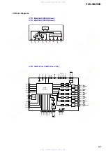
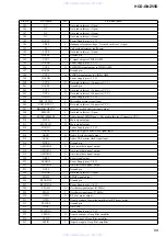
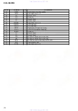
IC403 BH2210FV-E2 (SIGNAL IN/OUT CONTROL) (MAIN BOARD (2/4))
Pin No.
Pin Name
I/O
Pin Description
1
CTLIO
I
IN/OUT control port (Fixed at “H” in this set.)
2
RESET
I
Reset signal input
3
CLK
I
Serial data clock signal input
4
LATCH
I
Serial data latch signal input
5
TC-MUTE
O
Tape playback muting on/off control signal output “H”: muting on
6
NO USE
O
Not used. (Open)
7
REC MUTE
O
Recording muting on/off control signal output “L”: muting on
8
NO USE
O
Not used. (Open)
9
SM-NSP-MUTING
O
S master processor IC PWM 50% duty muting on/off control signal output
“L”: muting on
10
SM-SOFT-MUTING
O
S master processor IC soft muting on/off control signal output “L”: muting on
11
SM-PG-MUTE
O
S master processor IC PWM muting on/off control signal output “L”: muting on
12
SM-INIT
O
Initialization signal to the S master processor IC
13
LATCHO
O
Serial data latch output signal Not used. (Open)
14
CLKO
O
Serial data clock signal output Not used. (Open)
15
DO1
O
Serial data signal output 1 Not used. (Open)
16
DI2
I
Serial data signal input 2 Not used. (Connect to ground.)
17
A-TRIG
O
Deck A side trigger plunger drive signal output “H”: plunger on
18
CAMP-CNT
O
Capstan motor drive signal output
19
B-TRIG
O
Deck B side trigger plunger drive signal output “H”: plunger on
20
REC BIAS
O
Recording bias on/off control signal output “H”: bias on
21
TC RELAY
O
Recording/playback selection signal output “H”: recording, “L”: playback
22
ADC RESET
O
Power down control signal to analog to digital converter “L”: power down
23
NO USE
O
Not used. (Open)
24
FAN CTRL
O
Fan driving signal output “L”: fan on Not used in this set. (Open)
25
DO2
O
Not used. (Open)
26
DI1
I
Serial data signal input
27
VSS
—
Ground pin
28
VDD
—
Power supply pin (+3 V)
www. xiaoyu163. com
QQ 376315150
9
9
2
8
9
4
2
9
8
TEL 13942296513
9
9
2
8
9
4
2
9
8
0
5
1
5
1
3
6
7
3
Q
Q
TEL 13942296513 QQ 376315150 892498299
TEL 13942296513 QQ 376315150 892498299


