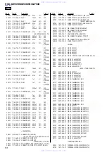


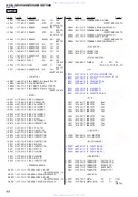


2
HCD-DZ555K/DZ556KB/DZ750K
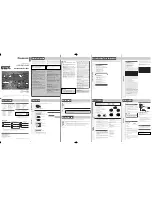
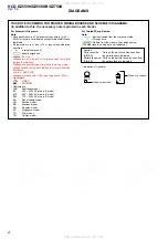
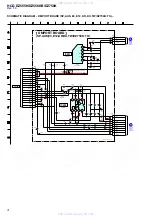
DIAGRAMS
For Schematic Diagrams.
Note:
• All capacitors are in
µ
F unless otherwise noted. (p: pF)
50 WV or less are not indicated except for electrolytics and
tantalums.
• All resistors are in
Ω
and
1
/
4
W or less unless otherwise
specified.
•
f
: internal component.
•
C
: panel designation.
THIS NOTE IS COMMON FOR PRINTED WIRING BOARDS AND SCHEMATIC DIAGRAMS.
(In addition to this, the necessary note is printed in each block.)
•
A
: B+ Line.
• Voltages are dc with respect to ground under no-signal
(detuned) conditions.
• Voltages are dc with respect to ground in service mode.
Voltage variations may be noted due to normal production
tolerances.
no mark : DVD STOP
• Voltages are taken with VOM (Input impedance 10 M
Ω
).
• Signal path.
L
: VIDEO
f
: AUDIO IN
• Abbreviation
AUS
: Australian model
E3
: 220 – 240V AC area in E model
E12
: 220 – 240V AC area in E model
E32
: 110 – 240V AC area in E model
EA
: Saudi Arabia model
KR
: Korean model
MX
: Mexican model
RU
: Russian model
SP
: Singapore model
TH
: Thai model
TW
: Taiwan model
For Printed Wiring Boards.
Note:
•
X
: parts extracted from the component side.
•
a
: Through hole.
•
: Pattern from the side which enables seeing.
(The other layers' patterns are not indicated.)
• Indication of transistor.
Caution:
Parts face side: Parts on the parts face side seen from
(SIDE A) the parts face are indicated.
Pattern face side: Parts on the pattern face side seen from
(SIDE B) the pattern face are indicated.
C
B
These are omitted.
E
Q
C E
B
These are omitted
www. xiaoyu163. com
QQ 376315150
9
9
2
8
9
4
2
9
8
TEL 13942296513
9
9
2
8
9
4
2
9
8
0
5
1
5
1
3
6
7
3
Q
Q
TEL 13942296513 QQ 376315150 892498299
TEL 13942296513 QQ 376315150 892498299