


– 66 –
KF-60DX100
K
RM-Y910
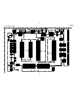
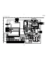
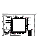
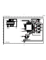
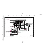
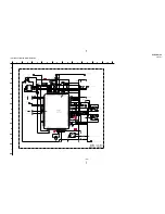
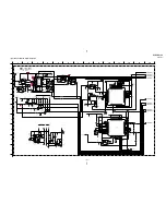
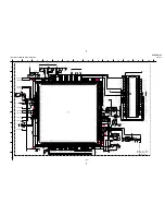
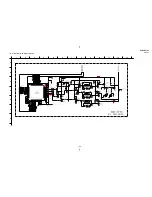
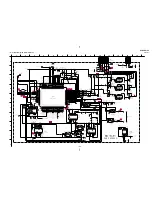
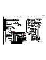
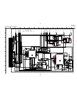
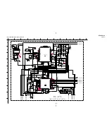
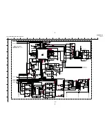
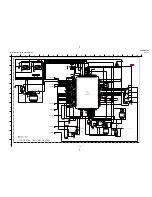
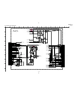
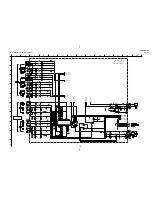
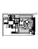
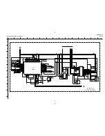
(13) Schematic Diagram of BC (1/3) Board
1
2
3
4
5
6
7
8
9
10
11
12
13
14
15
A
B
C
D
E
F
G
H
I
J
VIDEO
C
Y
Y/B-Y/R-Y
R/G/B
8
9
R/G/B
0
0
0
0
0
0
0
0
0
0
0
0
0
B
G
7
6
5
4
0
0
2.0
2.5
2.6
1.9
2.4
3.0
5.1
5.1
0.4
4.5
4.4
2.9
3.3
0
0
0
R
VIDEO
Y
B-Y
R-Y
R
G
B
3
2
1
3.6
3.6
3.6
2.5
3.2
2.9
3.0
2.6
2.3
1.9
1.7
1.9
4.9
4.5
4.5
2.9
2.5
0.5
2.1
3.4
0.5
0
1.3
2.0
2.1
Y
Y
C
2.1
1.5
3.1
3.7
3.1
3.7
0.1
2.5
1.5
2.1
1.9
1.3
0.5
0.4
1.3
1.9
Y/B-Y/R-Y
Y/B-Y/R-Y
VIDEO
Y
C
Y
R-Y
B-Y
B-Y
R-Y
Y
Y
C
Y/B-Y/R-Y
0
0
0.5
0.4
0.5
0
0
0.4
0.5
0.4
10
11
0.5
0.5
0.5
0.5
0.5
5.1
0.5
BUFFER
BUFFER
BUFFER
BUFFER
BUFFER
BUFFER
EXT R
EXT G
EXT B
YCBCRSW
R IN
G IN
B IN
SVCC
Y IN
CB IN
CR IN
APED
EXT Y
EXT CB
EXT CR
CLAMP
XTAL
APCFIL
SGND
FSC
Y CLAMP
CVCC
Y IN
C IN
MON OUT
ADRS
SDA
SCL
CGND
HVCC
Y1IN
TEST
AFCFIL
Y2IN
C1 IN
HGND
VTIM
SEL OUT
SYNC IN
SCP
HTIM
YSYM
YOUT
CBOUT
CROUT
TO BC(3/3)
CN1924
TO BC(3/3)
TO BC(1/3)
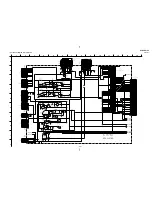
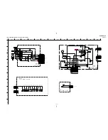
BUFF
INV
BUFF
BUFF
SW
BUFF
INV
BUFF
PD6
PD7
PC0
PC1
PC2
PC3
PC4
PC5
PC6
PC7
PF0
PF1
PF2
HP
VP
VSS
XTL
EXTL
CVSS
RST
PD5
PD4
PD3
PD2
PD1
PD0
PA4
PA3
bit3
bit2
bit1
PA5
LFC2
LFC1
VIN
CVDD
CAP
R
PB6
PB5
PB4
PB3
PB2
PB1
PB0
YS
XLC
EXLC
VDD
VDD
VSS
VSS
SDA
SCL
YM
PF7
PE0
PE1
PE2
PF3
PF5
G
B
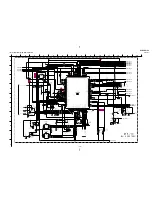
I
BUFF
BUFF
INH
GND
GND
HD-M
HD-S
VD-M
VD-S
VD-O2
V
CC
NC
NC
NC
NC
HD-O2
SEL1
SEL2
BUFF
TO BC(3/3)
TO BC(1/3)
SYNC_SEL
GND
GND
INH
CC
V
HD1
2151H
VD1
VD0 VS
2151V
SEL2
SEL1
NC
NC
NC
NC
B-SS844.<U/C>-BC.-P1-05
(SUB YCT,CCD,V-CHIP)
(SUB)
(SUB)
9Ch
66h
9V
9V
GND
FSC
BLOCK-M
BLOCK-S
GND
SUB C
GND
SUB Y
D1-CR
GND
D1-CB
GND
D1-Y
GND
D2-CR
GND
D2-CB
GND
D2-Y
DRC SEL2
DRC SEL1
5V
5V
RST
GND
GND
GND
CR
GND
CB
HD
VD
GND
GND
MID VD
MID HD
GND
SEL CB OUT
GND
SEL CR OUT
GND
SEL Y OUT
MAIN C
MAIN Y
YUV SW
SUB G
SUB YS
Y
M-FSC
GND
SCL1
SDA1
S-HD
S-VD
GND
GND
GND
GND
GND
GND
BC(1/3)
TO A(2/3)BOARD
MILD CONT
NC
VD0 HS
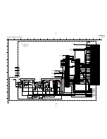
1
2
3
4
5
6
7
8
9
10 11 12
13
14
15
16
17
18
19
20
21
22
23
24
25
26
27
28
29
30
31
32
33
34
35
36
37
38
39
40
41
42
43
44
45
46
47
48
1
2
3
4
5
6
7
8
9
10
11
12
13
14
15
16
1
2
3
4
5
1
2
3
4
5
6
7
8
9
10
11
12
13
14
15
16
17
18
19
20
21
22
23
24
25
26
27
28
29
30
31
32
33
34
35
36
37
38
39
40
41
42
43
44
45
46
47
48
49
50
51
52
53
54
55
56
57
58
59
60
61
62
63
64
A1
A2
A3
A4
A5
A6
A7
A8
A9
A10
A11
A12
A13
A14
A15
A16
A17
A18
A19
A20
A21
A22
A23
A24
A25
A26
A27
A28
A29
A30
A31
A32
C1
C2
C3
C4
C5
C6
C7
C8
C9
C10
C11
C12
C13
C14
C15
C16
C17
C18
C19
C20
C21
C22
C23
C24
C25
C26
C27
C28
C29
C30
C31
C32
1
2
3
4
5
6
7
8
9
10
11
12
13
14
15
16
R3197
R3199
R3222
R3223
R3224
R3225
R3226
R3227
R3228
R3229
R3230
R3231
R3232
R3233
R3234
R3235
R3236
R3237
R3238
R3239
R3240
R3241
R3242
R3243
R3244
R3245
R3246
R3247
R3248
R3249
R3250
R3251
R3252
R3253
R3254
R3256
R3257
R3258
R3259
R3260
R3261
R3262
R3263
R3264
R3265
R3266
R3267
R3268
R3269
R3270
R3271
R3272
R3273
R3274
C3106
C3120
C3121
C3122
C3123
C3124
C3125
C3126
C3127
C3128
C3129
C3130
C3131
C3132
C3133
C3134
C3135
C3136
C3137
C3138
C3139
C3140
C3141
C3142
C3143
C3144
C3145
C3146
C3147
C3149
C3150
C3151
C3152
C3154
C3155
C3156
C3157
C3158
C3159
IC3009
IC3010
Q3053
Q3054
Q3055
Q3056
Q3057
Q3058
Q3059
Q3060
Q3061
Q3062
Q3063
Q3064
Q3065
Q3066
Q3067
Q3068
X3006
L3011
L3016
L3017
L3018
L3019
L3020
L3021
L3022
CN3001
D3003
D3004
IC3012
Q3078
R3296
R3297
R3298
R3139
IC3014
IC3005
R3304
R3255
C3148
C3153
X3005
CXA2103Q
YCT-SUB
15k 1/16W :CHIP
0.1
25V
F:CHIP
47
1/16W
:CHIP
47
1/16W
:CHIP
10k
1/16W
:CHIP
0.47
10V
B:CHIP
0.01
16V
B:CHIP
0.47
10V
B:CHIP
0.1
25V
F:CHIP
0.47 10V B:CHIP
0.01
16V
B:CHIP
0.47
10V
B:CHIP
1k
1/16W
:CHIP
0
:CHIP
1M
1/16W
:CHIP
220
1/16W
:CHIP
1k
1/16W
:CHIP
47
1/16W
:CHIP
47
1/16W
:CHIP
470
1/16W
:CHIP
10uH
:CHIP
0.1
25V
F:CHIP
10uH
:LAV35
#
CH:CHIP
0.1
25V
F:CHIP
100
1/16W
:CHIP
10uH
:CHIP
470
1/16W
:CHIP
100
1/16W
:CHIP
#
#
1/16W
:CHIP
4.7
0.1
25V
F:CHIP
10k
1/16W
:CHIP
1000p
25V
CH:CHIP
10k
1/16W
:CHIP
220p
CH:CHIP
0
:CHIP
220 1/16W
:CHIP
220
1/16W
:CHIP
220
1/16W
:CHIP
10uH
:CHIP
470
10V
10uH
:CHIP
CXP85840A-039Q
SUB-CCD V-CHIP
0.1
16V
B:CHIP
1000p
B:CHIP
0.0047
B:CHIP
15p
CH:CHIP
47
16V
2.2k
1/16W
:CHIP
2.2k
1/16W
:CHIP
2.2k
1/16W
:CHIP
330
1/16W
:CHIP
330
1/16W
:CHIP
330
1/16W
:CHIP
10
100
1/16W
:CHIP
100 1/16W :CHIP
#
F:CHIP
10uH
:CHIP
#
1/16W
:CHIP
#
1/16W
:CHIP
4.7k
1/16W
:CHIP
1.5k
1/16W
:CHIP
100
1/16W
:CHIP
1.5k
1/16W
:CHIP
4.7k
1/16W
:CHIP
1.5k
1/16W
:RN-CP
1.5k
1/16W
:RN-CP
12MHz
0
:CHIP
0
:CHIP
0.47
10V
B:CHIP
10k
1/16W
:CHIP
10k
1/16W
:CHIP
10k
1/16W
:CHIP
10k
1/16W
:CHIP
10k
1/16W
:CHIP
100
1/16W
:CHIP
#
1/16W
:CHIP
0
:CHIP
15p
CH:CHIP
100
1/16W
:CHIP
1k
1/16W
:CHIP
100
1/16W
:CHIP
0.1
16V
B:CHIP
0.1
16V
B:CHIP
0.1
16V
B:CHIP
1k
1/16W
:CHIP
10k
1/16W
:CHIP
# CH:CHIP
# CH:CHIP
0.1
16V
B:CHIP
12p
CH:CHIP
0.47
10V
B:CHIP
470p
CH:CHIP
0.1
16V
B:CHIP
0.1
16V
B:CHIP
0.1
16V
B:CHIP
47
16V
100
16V
10uH
:CHIP
10uH
:CHIP
64P
2SC2412K
2SC2412K
2SC2412K
2SC2412K
2SC2412K
2SC2412K
2SC2412K
2SC2412K
2SC2412K
2SC2412K
2SC2412K
2SC2412K
2SC2412K
2SA1037AK
2SA1037AK
MA113
MA113
SN74LV4053APWR
2SA1037K
100k
1/16W
:CHIP
470
1/16W
:CHIP
100 1/16W :CHIP
47
1/16W
:CHIP
TC7SH08FU
SN74LV4053APWR
DRC_SYNC_SEL
#
:CHIP
3.9k
1/16W
:CHIP
4.7
470u
10V
3.58MHz
BLOCK-S
5V
5V
5V
5V
5V
9V
5V
D COMP
9V
9V
MILD CONT
SEL 2
SEL 2
MILD CONT
YS
B
G
YS
R
G
B
S-HD
DAT1
CLK1
DAT1
CLK1
SUB-C
SUB-Y
R
S-VD
D2-Y
D2-CB
D2-CR
D1-Y
D1-CB
D1-CR
SUB G
SUB YS
SUB G
SUB-C
SUB-Y
SUB YS
CLK1
DAT1
S-VD
S-HD
S-VD
S-HD
Y
CR
CB
HD2
VD2
SEL CB
SEL CR
SEL Y
MAIN Y
MAIN C
VD3
HD3
VD3
HD3
HD2
CR
CB
Y
VD2
TO BC1/3,BC2/3_1
TO BC1/3,BC2/3_2
TO BC1/3,BC3/3_3
TO BC1/3,BC2/3_4
TO BC1/3,BC2/3_5
TO BC1/3,BC2/3_6
TO BC1/3,BC2/3_7
TO BC1/3,BC2/3_9
TO BC1/3,BC2/3_8
TO BC1/3,BC2/3_10
TO BC1/3,BC2/3_11
TO BC1/3,BC2/3_12
TO BC1/3,BC3/3_13
TO BC1/3,BC3/3_14
TO BC1/3,BC3/3_15
TO BC1/3,BC3/3_16
TO BC1/3,BC3/3_17
TO BC1/3,BC3/3_19
TO BC1/3,BC3/3_18
Summary of Contents for GRAND WEGA KF 60DX100
Page 88: ... 87 KF 60DX100 RM Y910 H2 USER CONTROL H2 BOARD Component Side H2 BOARD Conductor Side ...
Page 138: ......
Page 228: ......


