background image

DVP-S320

4-27

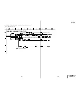
4-28

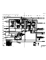
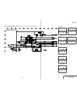
MB-82 (ARP)  SCHEMATIC  DIAGRAM

• See page 4-15 for printed wiring board.

– Ref. No.: MB-82 board; 1,000 series –

ARP

MB-82 (5/10)

• Waveforms

1

IC303 

 (DVD play)

500 mV/DIV

100 ns/DIV

1.6 Vp-p

2

IC303 

 (CD play)

500 mV/DIV

200 ns/DIV

1.6 Vp-p

Summary of Contents for DVP-S320

Page 1: ...MICROFILM SERVICE MANUAL Singapore Model CD DVD PLAYER DVP S320 RMT D109E SPECIFICATIONS Continued on next page ...

Page 2: ...tments or performance of procedures other than those specified herein may result in hazardous ra diation exposure SAFETY CHECK OUT 1 Check the area of your repair for unsoldered or poorly sol dered connections Check the entire board surface for solder splashes and bridges 2 Check the interboard wiring to ensure that no wires are pinched or contact high wattage resistors 3 Look for unauthorized rep...

Page 3: ...ic Diagram 4 21 MB 82 SERVO DSP Schematic Diagram 4 23 MB 82 DRIVE Schematic Diagram 4 25 MB 82 ARP Schematic Diagram 4 27 MB 82 SYSTEM CONTROL Schematic Diagram 4 29 MB 82 HGA Schematic Diagram 4 31 MB 82 CLOCK GENERATOR Schematic Diagram 4 33 MB 82 DAC Schematic Diagram 4 35 MB 82 BIAS Schematic Diagram 4 37 AU 208 Printed Wiring Board 4 39 AU 208 Schematic Diagram 4 41 FL 97 Printed Wiring Boar...

Page 4: ... shown below Set Case Page 2 1 Power Block Page 2 1 AU 208 Board Page 2 1 Mechanism Deck Page 2 2 Front Panel Page 2 2 Tray Cover Page 2 2 Optical Pick up Page 2 3 TK 51 Board Page 2 3 Belt Page 2 3 Loading Motor M001 MS 46 Board Page 2 3 Tray Page 2 2 MB 82 Board Page 2 1 ...

Page 5: ...See Fig 1 2 Open the side of case See Fig 1 3 Remove the case as lift straight See Fig 1 Fig 1 3 DISC REMOVAL PROCEDURE at POWER OFF 1 Insert a tapering driver into the aperture of the unit bottom and move the lever of chuck cam in the direction of the arrow A See Fig 2 2 Draw out the tray in the direction of the arrow B and remove a disc See Fig 2 Fig 2 Two screws Three screws Case Two screws Lev...

Page 6: ...1 1 SECTION 1 GENERAL This section is extracted from instruction manual 3 867 036 11 DVP S320 ...

Page 7: ...1 2 ...

Page 8: ...1 3 ...

Page 9: ...1 4 ...

Page 10: ...1 5 ...

Page 11: ...1 6 ...

Page 12: ...1 7 ...

Page 13: ...1 8 ...

Page 14: ...1 9 ...

Page 15: ...1 10 ...

Page 16: ...1 11 ...

Page 17: ...1 12 ...

Page 18: ...1 13 ...

Page 19: ...1 14 1 14 E ...

Page 20: ... S320 4 Case 3 Two screws 2 Two screws 1 Three screws 2 Two flat cables CN002 003 5 Flat cable CN006 7 MB 82 board 6 Four screws B3 3 Connector CN001 1 Connector CN011 4 Flat cable CN005 1 Connector CN101 2 Three connectors CN201 202 203 3 Four screws B3 4 Power block 5 Four screws B3 4 Four screws B3 2 Connector CN401 6 Harness FG 55 1 Connector CN201 3 Flat cable CN301 7 AU 208 board ...

Page 21: ...it bottom and move the lever of chuck cam in the direction of the arrow A 3 Two claws B A 2 Flat cable CN006 1 Connector CN203 3 Two screws B3 7 Claw 6 Claw 8 Front panel 4 Boss 5 Boss 2 Two flat cables CN003 004 3 Screw B3 4 Mechanism deck 1 Connector CN001 2 Chuck ass y 4 Remove the tray in the direction of the arrow B 3 Move the lever of chuck cam in the direction of the arrow A 1 Two screws BT...

Page 22: ...Remove the base unit holder in the direction of the arrow A 2 Two claws 1 Two flexible board CN001 002 5 Optical pick up 4 Three step screws A 2 Two screws B2 6 4 1 Belt 9 TK 51 board 8 Claw 7 Claw 6 Flexible board CN001 5 Flexible board CN002 3 Three claws 4 Loading motor M001 MS 46 board ...

Page 23: ...2 4 2 11 INTERNAL VIEW DC motor loading 1 541 632 11 Optical pick up KHM 220AAA J1RP 8 820 081 03 ...

Page 24: ...2 5 2 12 CIRCUIT BOARDS LOCATION 2 5 E Power Block HS 030SH SWITCHING REGULATOR TK 51 RF SERVO AU 208 AUDIO MB 82 SIGNAL PROCESS SERVO FL 97 FUNCTION SWITCH MS 46 LOADING FR 146 IR POWER SWITCH ...

Page 25: ...G COIL TILT MOTOR DRIVE IC601 HGA Serial BUS CURSOR UNIT SW REG 12V EVER5V 3 3V 5V A 12V M 12V 3 3V 5V 12V 12V EVER5V SWITCH SWITCH ND201 IC201 IF CON IC701 IC202 IC802 SPINDLE SLED LOADING MOTOR DRIVE CDDOUT CDDATA CDBCK CDLRCK IC303 ARP2 SD 0 7 RF IC401 AV DECODER IC304 16M DRAM IC402 403 16M SDRAM IC204 1M SRAM IC201 4K EEP ROM IC206 16M FLASH IC902 AUDIO 2CH DAC SPDIF Parallel BUS VIDEO V VIDE...

Page 26: ... DAB 2 3 GIO 1 2 PWM 0 2 TRD TILT MUTE FGMODE FCD TLTA TLTB 117 ı 120 122 ı 125 74 81 84 93 96 15 ı 18 13 14 2 3 23 26 FOCUS COIL DRIVE TILT MOTOR DRIVE Q802 803 GAIN CONTROL TRD FCD TLTA TLTB 7 9 20 IC801 IC701 IC702 1 2 11 ı 14 15 16 17 18 SPINDLE MOTOR DRIVE LOADING MOTOR DRIVE SLED MOTOR DRIVE SLDA SLDB STVC 3 3V 2 5VC 2VC 1 6VC 5V 20 26 23 IC802 3 1 IC702 2 2 3 3V 7 5 IC803 1 2 IC803 2 2 14 1...

Page 27: ...6 139 141 144 146 147 134 135 137 138 140 141 143 144 146 147 149 150 152 153 155 156 105 108 110 113 115 118 120 123 125 127 129 132 148 150 152 63 68 70 71 HA 0 21 HD 0 15 IC402 403 16M SDRAM DDT 0 15 DAD 0 11 107 ı 110 29 ı 32 47 ı 51 91 93 ı 96 97 98 100 ı 105 SD 0 7 SD 0 7 DT 0 7 I SDCK SDEF XSHD XSAK XSRQ CDDOUT CDDATA CDBCK CDLRCK 38 ı 43 45 46 166 167 193 194 196 198 ı 202 168 170 172 178 ...

Page 28: ... 4A 2A 1A 4Y 2Y 1Y SC1 SO1 SC1 SO1 CS0L SC0 SO0 SI0 XFRRST IFSI0 XFRRST XIFINT LDMP DMP LDMM DMM OCSW1 OCSW2 CKSW1 FCSON SPDLSTOP SPGAIN XDRVMUTE LDMP DMP LDMM DMM OCSW1 OCSW2 CKSW1 94 93 92 91 64 63 88 XDACRST MA MUTE MA MUTE 26 49 126 133 146 154 PLL IC001 IC003 IC004 N27MHGA RF SERVO SEE PAGE 3 4 SIGNAL PROCESS VIDEO SEE PAGE 3 5 RST CS2 CS3 CE CS WE RD WR0 WR1 PF7 CS4 CS1 CS0 MD ML XT1 05 SCKO...

Page 29: ...SO1 SC1 SO1 SC1 XDACS0 BCK LRCK ACH12 SYSTEM CONTROL SEE PAGE 3 7 8 XDACRST 384FSDA 05 AU 208 BOARD 2 2 SEE PAGE 4 41 15 11 13 10 19 9 7 LPF 6dB 5 7 3 1 14 18 16 19 10 20 22 1 Q435 436 MUTE Q301 Q305 Q303 304 MUTE CONTROL DIGITAL OUT Q341 BUFFER D IN IC431 IC505 J505 J502 L AUDIO OUT1 OPTICAL COAXIAL R L AUDIO OUT2 R CN005 CN301 A MUTE MA MUTE A MUTE MA MUTE SPDIF SPDIF AUDIOLT AUDIORT ZFLT ZFRT I...

Page 30: ... SOUT1 SIN1 SBUSY1 SRDY1 FRRST N V MUTE A MUTE N X IN X OUT IFSC0 SYSTEM CONTROL SEE PAGE 3 8 SIGNAL PROCESS VIDEO SEE PAGE 3 5 AUDIO SEE PAGE 3 9 IFSI0 IFSO0 XVIFCS XIFINT XFRRST V MUTE A MUTE 6 4 5 3 2 8 9 1 6 4 5 3 2 15 15 8 9 1 4 CN201 6 7 3 70 6 9 31 32 71 72 76 78 8 11 12 77 10 AN1 AN0 5 3 3V 3 3V 5V CN203 LEFT RIGHT UP DOWN ENTER DIG1 13 SEG1 17 DVD MENU S215 RETURN S216 PREV S217 NEXT S218...

Page 31: ...8 CN201 F1 F2 VEE EVER5V PCONT CN202 9 12 3 3V PCONT 05 10 5 8 CN002 9 12 10 5 Q201 30V REG IC202 ND201 Q001 002 T001 DC DC CONVERTER IC201 IC051 15 PCONT EVER5V 12V 15 CN001 5 1 2 4 B301 12V 12V 5V EVER5V 3 3V 6 1 2 7 5 CN001 5V 3 3V V3 3V CN006 A 12V A 5V S12V 3 3V A 12V M 12V 5V 3 3V 2 1 IC301 8V REG IC302 9V REG IC321 IC505 EVER5V 3 3V IC404 3 3 REG IC904 A 5V REG IC801 IC802 IC401 IC203 IC702...

Page 32: ...V or less are not indicated except for electrolytics and tantalums All variable and adjustable resistors have characteristic curve B unless otherwise noted 2 nonflammable resistor 5 fusible resistor C panel designation internal component C adjustment for repair U B Line V B Line Circled numbers refer to waveforms Voltages are dc between measurement point Readings are taken with a color bar signals...

Page 33: ...DVP S320 FRAME 1 2 4 3 4 4 4 1 FRAME SCHEMATIC DIAGRAM FRAME 1 SCHEMATIC DIAGRAM ...

Page 34: ...DVP S320 4 5 4 6 FRAME 2 SCHEMATIC DIAGRAM FRAME 2 2 ...

Page 35: ...part isn t mounted in this model is printed on this diagram TK51 BOARD SIDE A CN001 B 2 CN002 C 2 CN003 D 2 CN004 D 3 D003 B 2 IC001 C 1 Q001 A 2 Q002 D 1 Power Block HS 030SH SWITCHING REGULATOR TK 51 RF SERVO AU 208 AUDIO MB 82 SIGNAL PROCESS SERVO FL 97 FUNCTION SWITCH MS 46 LOADING FR 146 IR POWER SWITCH CN003 1 672 677 12 TK 51 BOARD SIDE A 12 A B C D 1 2 3 05 C E B C E B ...

Page 36: ...1 ª CD play 200 mV DIV 20 ms DIV 448 mVp p 5 IC001 ª DVD play 500 mV DIV 50 ms DIV 1 3 Vp p 6 IC001 ª CD play 500 mV DIV 200 ms DIV 1 7 Vp p 7 IC001 º DVD play 100 mV DIV 50 ms DIV 180 mVp p 8 IC001 º CD play 500 mV DIV 50 ms DIV 860 mVp p 9 IC001 DVD play 500 mV DIV 100 ns DIV 1 5 Vp p º IC001 CD play 500 mV DIV 500 ns DIV 1 5 Vp p RF SERVO TK 51 1 672 677 12 TK 51 BOARD SIDE B 12 05 ...

Page 37: ...IAGRAM See page 4 7 for printed wiring board and page 4 10 for waveforms Ref No TK 51 board 2 000 series RF SERVO TK 51 Note The components identified by mark or dotted line with mark are critical for safety Replace only with part number specified ...

Page 38: ...es that the part isn t mounted in this model is printed on this diagram LOADING MS 46 05 1 675 146 11 MS 46 BOARD 11 CHUCK SENSOR LOADING MOTOR S001 TRAY SENSOR CN001 S001 Power Block HS 030SH SWITCHING REGULATOR TK 51 RF SERVO AU 208 AUDIO MB 82 SIGNAL PROCESS SERVO FL 97 FUNCTION SWITCH MS 46 LOADING FR 146 IR POWER SWITCH ...

Page 39: ...202 A 5 IC206 A 6 IC302 D 3 IC303 C 4 IC401 C 2 IC601 A 4 IC701 C 5 IC904 A 1 Q801 C 5 Q802 C 6 Q803 C 6 There are few cases that the part isn t mounted in this model is printed on this diagram SIGNAL PROCESS SERVO MB 82 1 672 676 23 MB 82 BOARD SIDE A 23 A B C D 1 2 3 4 5 6 05 B C E B C E A K K A A K A K K C B E K A A 5 4 1 2 3 Power Block HS 030SH SWITCHING REGULATOR TK 51 RF SERVO AU 208 AUDIO ...

Page 40: ...2 MB 82 BOARD SIDE B D701 C 2 D806 C 2 IC005 A 6 IC201 A 3 IC203 A 3 IC204 B 2 IC207 A 2 IC304 C 3 IC402 C 5 IC403 C 5 IC404 D 5 IC702 B 1 IC801 C 2 IC802 C 1 IC803 C 1 IC902 A 6 1 672 676 23 MB 82 BOARD SIDE B 23 A B C D 1 2 3 4 5 6 05 1 2 3 5 4 ...

Page 41: ...DVP S320 4 19 4 20 MB 82 AV DECODER SCHEMATIC DIAGRAM See page 4 15 for printed wiring board Ref No MB 82 board 1 000 series AV DECODER MB 82 1 10 ...

Page 42: ...VP S320 4 21 4 22 MB 82 SDRAM SCHEMATIC DIAGRAM See page 4 15 for printed wiring board Ref No MB 82 board 1 000 series SDRAM MB 82 2 10 Waveforms 1 IC401 1 1 Vp p H 2 IC401 816 mVp p H 3 IC401 1 2 Vp p H ...

Page 43: ...rinted wiring board Ref No MB 82 board 1 000 series Waveforms 1 IC701 ª DVD play 500 mV DIV 50 ms DIV 1 4 Vp p 2 IC701 ª CD play 500 mV DIV 200 mV DIV 1 7 Vp p 3 IC701 DVD play 100 mV DIV 5 ms DIV 180 mVp p 4 IC701 CD play 500 mV DIV 50 ms DIV 860 mVp p SERVO DSP MB 82 3 10 ...

Page 44: ...DVP S320 4 25 4 26 MB 82 DRIVE SCHEMATIC DIAGRAM See page 4 15 for printed wiring board Ref No MB 82 board 1 000 series DRIVE MB 82 4 10 ...

Page 45: ...MB 82 ARP SCHEMATIC DIAGRAM See page 4 15 for printed wiring board Ref No MB 82 board 1 000 series ARP MB 82 5 10 Waveforms 1 IC303 DVD play 500 mV DIV 100 ns DIV 1 6 Vp p 2 IC303 ª CD play 500 mV DIV 200 ns DIV 1 6 Vp p ...

Page 46: ...0 4 29 4 30 SYSTEM CONTROL MB 82 6 10 MB 82 SYSTEM CONTROL SCHEMATIC DIAGRAM See page 4 15 for printed wiring board Ref No MB 82 board 1 000 series Waveforms 1 IC202 2 4 Vp p 12 5 MHz 2 IC202 5 4 Vp p 25 3 MHz ...

Page 47: ...DVP S320 4 31 4 32 MB 82 HGA SCHEMATIC DIAGRAM See page 4 15 for printed wiring board Ref No MB 82 board 1 000 series HGA MB 82 7 10 ...

Page 48: ... board 1 000 series CLOCK GENERATOR MB 82 8 10 Waveforms 1 IC004 2 7 4 2 Vp p 26 9 MHz 2 IC003 7 DVD 6 2 Vp p 37 0 MHz CD 5 Vp p 33 6 MHz 3 IC001 6 4 2 Vp p 27 0 MHz 4 IC001 4 6 Vp p 33 8 MHz 5 IC001 DVD 5 8 Vp p 36 5 MHz CD 5 1 Vp p 33 8 MHz 6 IC001 DVD play 4 2 Vp p 25 3 MHz 7 IC001 CD play 4 7 Vp p 22 5 MHz ...

Page 49: ...DVP S320 4 35 4 36 MB 82 DAC SCHEMATIC DIAGRAM See page 4 15 for printed wiring board Ref No MB 82 board 1 000 series DAC MB 82 9 10 ...

Page 50: ...DVP S320 4 37 4 38 MB 82 BIAS SCHEMATIC DIAGRAM See page 4 15 for printed wiring board Ref No MB 82 board 1 000 series BIAS MB 82 10 10 ...

Page 51: ...6 D432 B 6 IC301 C 11 IC302 A 11 IC321 B 4 IC431 B 7 IC505 A 1 Q301 B 5 Q303 A 11 Q304 B 2 Q305 B 5 Q321 B 5 Q322 B 5 Q341 A 1 Q435 C 6 Q436 B 6 AUDIO VIDEO BUFFER AU 208 There are few cases that the part isn t mounted in this model is printed on this diagram Waveforms 1 IC321 2 1 1 Vp p H 2 IC321 4 1 2 Vp p H Power Block HS 030SH SWITCHING REGULATOR TK 51 RF SERVO AU 208 AUDIO MB 82 SIGNAL PROCES...

Page 52: ...DVP S320 4 41 4 42 AUDIO VIDEO BUFFER AU 208 AU 208 AUDIO VIDEO BUFFER SCHEMATIC DIAGRAM Ref No AU 208 board 2 000 series ...

Page 53: ... 10 Q201 B 1 There are few cases that the part isn t mounted in this model is printed on this diagram 1 672 260 13 FL 97 BOARD 13 A B C 1 2 3 4 5 6 7 8 9 10 11 12 13 FLUORESCENT INDICATOR TUBE NEXT OPEN CLOSE 1 3 4 5 17 S218 PREV S217 1 TITLE DVD MENU RETURN 1 9 05 Power Block HS 030SH SWITCHING REGULATOR TK 51 RF SERVO AU 208 AUDIO MB 82 SIGNAL PROCESS SERVO FL 97 FUNCTION SWITCH MS 46 LOADING FR...

Page 54: ...DVP S320 4 45 4 46 FL 97 FUNCTION SWITCH SCHEMATIC DIAGRAM Ref No FL 97 board 2 000 series FUNCTION SWITCH FL 97 1 2 ...

Page 55: ...DVP S320 4 47 4 48 FL 97 IF CON SCHEMATIC DIAGRAM See page 4 43 for printed wiring board Ref No FL 97 board 2 000 series Waveform 1 IC201 3 9 Vp p 4 MHz IF CON FL 97 2 2 ...

Page 56: ...odel is printed on this diagram FR 146 BOARD CN001 B 3 CN002 A 5 D001 A 4 D002 A 4 D003 B 4 D004 A 4 D071 A 1 IC051 A 1 Q001 A 3 Q002 A 3 IR POWER SWITCH FR 146 05 1 672 261 13 FR 146 BOARD 13 ON STANDBY 3 2 1 A B 1 2 3 4 Power Block HS 030SH SWITCHING REGULATOR TK 51 RF SERVO AU 208 AUDIO MB 82 SIGNAL PROCESS SERVO FL 97 FUNCTION SWITCH MS 46 LOADING FR 146 IR POWER SWITCH ...

Page 57: ... 2 D183 C 2 D184 C 2 D185 C 3 D211 B 1 D212 B 2 D311 A 2 D401 C 1 D402 C 1 D511 B 2 D611 B 2 IC301 A 2 IC401 C 1 Q101 B 3 Q102 A 3 Q103 B 3 Q131 A 2 Q181 C 2 Q182 C 3 Q183 C 2 SWITCHING REGULATOR HS 030SH There are few cases that the part isn t mounted in this model is printed on this diagram Power Block HS 030SH SWITCHING REGULATOR TK 51 RF SERVO AU 208 AUDIO MB 82 SIGNAL PROCESS SERVO FL 97 FUNC...

Page 58: ...5k R401 68 D401 11EQS04 C401 100uF 35V D402 RD7 5ESB1 C107 330pF 250V C103 330pF 250V C104 330pF 250V D211 S2L20U L211 10uH C211 330uF 35V C213 47uF 35V D311 21DQ04 D611 D3S4M L311 10uH L611 39uH C611 560uF 35V C311 330uF 35V D511 S2L20U R301 68 C511 1000uF 25V D212 RD24FB2 L511 10uH C313 47uF 35V C512 47uF 35V P311 2 0A 60V P611 1 5A 60V P211 500mA 60V R304 1 5k R305 SHORT R306 1 5k R303 1k C301 ...

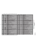
Page 59: ... signal to DAC L and R 100 PB4 O DVD CD select H 44 1kHz L 48kHz 5 1 SYSTEM CONTROL PIN FUNCTION MB 82 BOARD IC202 Pin No Pin name I O Function 1 PB5 O Analog filter gain control 2 PB6 O VES gain control H VES 3 PB7 O Rear CH boost control H rear boost 4 VCC3 Power supply 5 CLK O CPU clock out 25 MHz 6 CS5 O Not used 7 CS4 O Chip select signal for ARP SERVO DSP and HGA 8 CS3 O Chip select signal f...

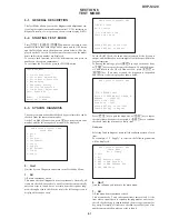
Page 60: ...t at a certain item that requires judg ment through a visual check to the result the following screen is displayed for the key entry Syscon Diagnosis Diag All Check No 2 Version 2 3 ROM Check Sum Check Sum xxxx Press NEXT Key to Continue Press PREV Key to Repeat _ For the ROM Check the check sum calculated by the Syscon is output and therefore you must compare it with the specified value for confi...

Page 61: ...aution Do not conduct this test with a mechanical deck connected The maximum voltage is applied to the Servo Driver IC IC801 IC802 If mechanical deck is connected the mo tor and optics could be damaged Disconnect mechanical deck following the output message then enter specified 4 or 5 digit number from the remote commander and press the ENTER The test is conducted only when the input data accord C...

Page 62: ...e data stored in ROM are copied to all areas of RAM IC304 connected to the ARP IC303 through the bus then they are read and checked if they ac cord If the detail check was selected initially the data are written to all areas and read then the same test is conducted once again with the data where all bits are inverted between 1 and 0 If discord is detected faulty address written data and read data ...

Page 63: ... 2 ARP 1930 8 3 Test Tone Error Codes List 00 Error not detected 01 RAM write read data discord 02 Gate array NG 03 EEPROM NG 08 ARP register read data discord 09 ARP RAM data bus error 10 ARP RAM address bus error 11 ARP RAM read data discord 12 Servo DSP NG 13 1930 SDRAM NG 14 ARP 1930 video NG 15 ARP 1930 audio NG 16 1910 UCODE download NG 17 System call error function not supported 18 System c...

Page 64: ...ough the message to con firm whether discs other than SACD disc are adjusted is not dis played you can finish the adjustment if pressing the STOP but ton During adjustment of each disc the measurement for disc type judgment is made As automatic adjustment does not judge the disc type unlike conventional models take care not to insert wrong type discs Also do not give a shock during adjustment 1 DV...

Page 65: ...llowing steps then adjusted values will be written to the EEPROM DVD Dual Layer Disc Adjustment Steps 1 Sled Tilt Reset 2 Disc Check Memory DL 3 Wait 500 msec 4 Set Disc Type DL 5 LD ON 6 Spdl Start 7 Wait 1 sec Layer 1 Adjust 8 Focus Servo ON 0 9 Auto Track Offset Adjust 10 Clva ON 11 Wait 500 msec 12 Tracking ON 13 Wait 500 msec 14 Sled ON 15 Check CLV Lock 16 Auto Loop Filter Offset Auto Focus ...

Page 66: ...rol and adjustment can be executed manually Drive Manual Operation Operation Menu 1 Disc type 2 Servo Control 3 Track Layer Jump 4 Manual Adjustment 5 Auto Adjustment 6 Memory Check 0 Disc Check Memory Exit Return In using the manual operation menu take care of the following points These commands do not provide protection thus requiring correct operation The sector address or time code field is di...

Page 67: ...isplay field will appear as shown below These values are displayed when PLL is locked Disc Type 1 Disc Type Auto Check 2 DVD SL 12 cm 3 DVD DL 12 cm 4 CD 12cm 5 SACD 12 cm 6 DVD SL 8 cm 7 DVD DL 8 cm 8 CD 8 cm 9 SACD 8 cm 0 Reset SLED TILT SA SI EMG 00 DVD SL 12 cm Display when DVD SL 12cm disc was selected Disc Type 1 Disc Type Auto Check 2 DVD SL 12 cm 3 DVD DL 12 cm 4 CD 12cm 5 SACD 12 cm 6 DVD...

Page 68: ... range of 10 to 80 If extreme value such as 00 or FF is set adjustment will be faulty In such a case check for disc scratch or cable dis connection then perform adjustment again 6 6 MECHA AGING Mecha Aging Press OPEN key Abort STOP key On the Test Mode Menu screen selecting 3 executes the aging of mechanism First open the tray and load a disc Press the PLAY key and the aging will start When the tr...

Page 69: ... made a request to seek nonexistent address 61 With a CD disc Syscon made a request to seek nonexistent address 62 With a CD disc Syscon made a request to seek nonexistent track No and index No 63 With a DVD disc seeking of target address failed 64 With a CD disc seeking of target address failed 65 With a CD disc seeking of target index failed 70 With a DVD disc physical information data could not...

Page 70: ...SECTION 7 ELECTRICAL ADJUSTMENTS DVP S320 In making adjustment refer to 7 4 Adjustment Related Parts Arrangement Note During diagnostic check the characters and color bars can be seen only with the NTSC monitor Therefore for diag nostic check use the monitor that supports both NTSC and PAL modes This section describes procedures and instructions necessary for adjusting electrical circuits in this ...

Page 71: ... be displayed correctly in spite of connection to the TV with a S terminal cable Mode Video level adjustment in test mode Signal Color bars Test point S VIDEO OUT S Y connector 75 Ω terminated Instrument Oscilloscope Specification 1 0 0 1 Vp p Checking method 1 In the test mode initial menu 6 Video Level Adjustment set so that color bars are generated 2 Confirm that the S Y level is 1 0 0 1 Vp p F...

Page 72: ...7 4 E 7 3 ADJUSTMENT RELATED PARTS ARRANGEMENT MB 82 BOARD SIDE A HS 030SH BOARD SIDE A 1 2 27 28 CN005 RV401 VIDEO LEVEL ADJ 1 1 7 6 CN202 CN203 ...

Page 73: ...and packing materials are given in the last of the electrical parts list SECTION 8 REPAIR PARTS LIST 8 1 EXPLODED VIEWS DVP S320 The components identified by mark or dotted line with mark are critical for safety Replace only with part number specified 8 1 1 CASE ASSEMBLY Ref No Part No Description Remark Ref No Part No Description Remark 7 4 4 4 6 1 2 3 8 3 5 Front panel section 1 3 975 726 81 EMB...

Page 74: ... 054 221 01 WINDOW FL 103 3 974 997 41 WINDOW REMOTE CONTROL 104 4 963 404 41 EMBLEM 5 A SONY 105 3 053 954 21 BUTTON POWER 106 3 053 955 01 INDICATOR POWER 107 4 951 620 01 SCREW 2 6X8 BVTP 108 3 054 651 11 BUTTON OPEN 109 3 054 220 11 BUTTON PLAY 110 3 053 504 11 CUSHION 111 1 771 564 11 SWITCH TACTILE 112 3 053 496 01 STICK L CURSOR 113 A 6065 300 A FR 146 BOARD COMPLETE 114 1 790 167 11 CABLE ...

Page 75: ...MPLETE 152 3 970 608 01 SUMITITE B3 BV 153 1 790 166 11 CABLE FLEXIBLE FLAT FMT 25 154 1 790 163 11 CABLE FLEXIBLE FLAT FMA 7 155 1 468 359 11 POWER BLOCK HS 030SH 156 1 769 744 91 CORD POWER 157 4 966 267 11 BUSHING FBS001 CORD 158 A 6065 302 A AU 208 BOARD COMPLETE 159 3 970 608 51 SUMITITE B3 BV 160 3 055 791 01 SUMITITE B3 RING BV 161 3 055 418 01 COVER EJECT 162 3 054 650 01 SPRING EMC 163 3 ...

Page 76: ...841 11 PULLEY GEAR 205 3 053 840 01 CAM DRIVING GEAR 206 3 053 839 01 TRAY DRIVING GEAR 207 4 974 711 01 SCREW 2X5 P TYIGHT PTTWH 208 3 053 842 01 BELT 209 3 053 849 01 SPRING TENSION 210 3 053 838 01 CHUCK CAM 211 3 053 836 11 BASE UNIT HOLDER 212 3 053 835 11 BASE LOADING 213 A 6066 013 A MS 46 BOARD COMPLETE 214 3 053 845 01 CHUCK PLATE 215 3 053 844 01 YOKE 216 3 053 848 11 CHUCK HOLDER 217 3 ...

Page 77: ... CHIP 18PF 5 50V C361 1 164 346 11 CERAMIC CHIP 1uF 16V C363 1 164 346 11 CERAMIC CHIP 1uF 16V C401 1 104 665 11 ELECT 100uF 20 10V C404 1 104 665 11 ELECT 100uF 20 10V C431 1 104 664 11 ELECT 47uF 20 16V C432 1 104 664 11 ELECT 47uF 20 16V C433 1 104 665 11 ELECT 100uF 20 10V C434 1 163 021 91 CERAMIC CHIP 0 01uF 10 50V C435 1 104 665 11 ELECT 100uF 20 10V C436 1 163 131 00 CERAMIC CHIP 390PF 5 5...

Page 78: ...R303 1 216 042 00 METAL CHIP 510 5 1 10W R305 1 216 073 00 METAL CHIP 10K 5 1 10W R307 1 216 073 00 METAL CHIP 10K 5 1 10W R309 1 216 097 91 RES CHIP 100K 5 1 10W R318 1 216 097 91 RES CHIP 100K 5 1 10W R321 1 216 073 00 METAL CHIP 10K 5 1 10W R322 1 216 073 00 METAL CHIP 10K 5 1 10W R323 1 216 021 00 METAL CHIP 68 5 1 10W R324 1 216 021 00 METAL CHIP 68 5 1 10W R325 1 216 021 00 METAL CHIP 68 5 1...

Page 79: ... 91 SHORT 0 JR218 1 216 295 91 SHORT 0 JR219 1 216 295 91 SHORT 0 JR220 1 216 295 91 SHORT 0 JR224 1 216 296 91 SHORT 0 JR226 1 216 295 91 SHORT 0 JR229 1 216 296 91 SHORT 0 JR230 1 216 296 91 SHORT 0 JR231 1 216 295 91 SHORT 0 JR233 1 216 296 91 SHORT 0 JR234 1 216 295 91 SHORT 0 JR235 1 216 295 91 SHORT 0 JR236 1 216 295 91 SHORT 0 JR237 1 216 295 91 SHORT 0 JR238 1 216 296 91 SHORT 0 JR244 1 21...

Page 80: ...70 11 CERAMIC CHIP 0 01uF 10 25V R259 1 216 025 91 RES CHIP 100 5 1 10W R260 1 216 025 91 RES CHIP 100 5 1 10W R261 1 216 025 91 RES CHIP 100 5 1 10W R262 1 216 025 91 RES CHIP 100 5 1 10W R264 1 216 073 00 METAL CHIP 10K 5 1 10W R266 1 216 073 00 METAL CHIP 10K 5 1 10W R267 1 216 049 91 RES CHIP 1K 5 1 10W R268 1 216 089 91 RES CHIP 47K 5 1 10W R270 1 216 073 00 METAL CHIP 10K 5 1 10W R271 1 216 ...

Page 81: ... 1 126 209 11 ELECT CHIP 100uF 20 4V C443 1 162 970 11 CERAMIC CHIP 0 01uF 10 25V C601 1 125 822 11 TANTALUM 10uF 20 10V C602 1 162 970 11 CERAMIC CHIP 0 01uF 10 25V C603 1 162 970 11 CERAMIC CHIP 0 01uF 10 25V C604 1 162 970 11 CERAMIC CHIP 0 01uF 10 25V C605 1 162 970 11 CERAMIC CHIP 0 01uF 10 25V C606 1 162 970 11 CERAMIC CHIP 0 01uF 10 25V C607 1 162 970 11 CERAMIC CHIP 0 01uF 10 25V C608 1 16...

Page 82: ...TOR CHIP 0uH FB055 1 500 283 11 INDUCTOR CHIP 0uH FB056 1 500 283 11 INDUCTOR CHIP 0uH FB058 1 500 283 11 INDUCTOR CHIP 0uH FB060 1 500 283 11 INDUCTOR CHIP 0uH FB080 1 216 801 11 METAL CHIP 22 5 1 16W FB081 1 216 801 11 METAL CHIP 22 5 1 16W FB083 1 216 801 11 METAL CHIP 22 5 1 16W FB084 1 216 801 11 METAL CHIP 22 5 1 16W FB085 1 216 801 11 METAL CHIP 22 5 1 16W FB087 1 216 801 11 METAL CHIP 22 5...

Page 83: ... 5 1 16W R313 1 216 833 91 RES CHIP 10K 5 1 16W R314 1 216 833 91 RES CHIP 10K 5 1 16W R315 1 216 833 91 RES CHIP 10K 5 1 16W R316 1 218 855 11 METAL CHIP 2 2K 0 50 1 16W R317 1 218 871 11 METAL CHIP 10K 0 50 1 16W R318 1 216 849 11 METAL CHIP 220K 5 1 16W R319 1 216 831 11 METAL CHIP 6 8K 5 1 16W R320 1 218 853 11 METAL CHIP 1 8K 0 50 1 16W R321 1 218 847 11 METAL CHIP 1K 0 50 1 16W R322 1 218 87...

Page 84: ...830 11 METAL CHIP 5 6K 5 1 16W R827 1 216 851 11 METAL CHIP 330K 5 1 16W R828 1 216 837 11 METAL CHIP 22K 5 1 16W R829 1 216 837 11 METAL CHIP 22K 5 1 16W R831 1 216 833 91 RES CHIP 10K 5 1 16W R832 1 216 833 91 RES CHIP 10K 5 1 16W R834 1 216 847 11 METAL CHIP 150K 5 1 16W R835 1 216 847 11 METAL CHIP 150K 5 1 16W R836 1 216 847 11 METAL CHIP 150K 5 1 16W R837 1 216 844 11 METAL CHIP 82K 5 1 16W ...

Page 85: ...TRANSISTOR 2SK2663 Q182 8 729 023 98 TRANSISTOR 2SC3377 Q183 8 729 046 40 TRANSISTOR 2SK2663 RESISTOR R152 1 219 121 21 FUSIBLE 0 22 1 4W F A 6065 275 A TK 51 BOARD COMPLETE Ref No 2 000 Series CAPACITOR C004 1 107 826 91 CERAMIC CHIP 0 1uF 10 16V C005 1 162 966 11 CERAMIC CHIP 0 0022uF 10 50V C006 1 124 779 00 ELECT CHIP 10uF 20 16V C007 1 162 966 11 CERAMIC CHIP 0 0022uF 10 50V C008 1 162 966 11...

Page 86: ... 16W R014 1 216 864 11 METAL CHIP 0 5 1 16W R015 1 216 833 91 RES CHIP 10K 5 1 16W R016 1 216 833 91 RES CHIP 10K 5 1 16W R017 1 216 829 11 METAL CHIP 4 7K 5 1 16W R018 1 216 833 91 RES CHIP 10K 5 1 16W R022 1 216 811 11 METAL CHIP 150 5 1 16W R023 1 216 820 11 METAL CHIP 820 5 1 16W R025 1 216 813 11 METAL CHIP 220 5 1 16W R026 1 216 864 11 METAL CHIP 0 5 1 16W R029 1 216 861 11 METAL CHIP 2 2M 5...

Page 87: ... 132 DVP S320 Sony Corporation Home Video Company 9 921 728 11 99G05091 1D Printed in Japan 1999 7 Published by Quality Assurance Dept ...

Reviews: