
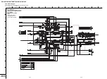


5-3
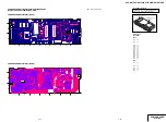
DVP-NS72HP/NS77H/NS77HP/NS78H/NS78HP
Pin No.
Pin name
Type
Function
103
CKSW
Input, SMT
Chuck Switch (H:Tray Open, L:Tray Closed)
104
OCSW
Input, SMT
Open/Close Switch (H:Tray Open, L:Tray Closed)
105
RXD
Input, SMT
Hardwared RS232C RXD
106
TXD
Output, SMT
Hardwared RS232C TXD
107
ICE
Input, SMT, PU
ICE mode enable
108
XSYSRST
Input
MT1389 reset input, active Low
109
IR
Input, SMT
IR control signal input
110
XIFBSY
Input, PD, SMT
Ext. CPU Ready/Busy interrupt signal (H: Busy, L: Ready)
111
DQM0
Output
Mask for DRAM input/output byte 0
112
EEWP
Output, PD, SMT
EEPROM Write Protect control (L : write allowed)
113
RD7
Output
DRAM data bit7
114
RD6
Output
DRAM data bit6
115
RD5
Output
DRAM data bit5
116
RD4
Output
DRAM data bit4
117
RD3
Output
DRAM data bit3
118
DVDD33
Power
3.3V power pin for internal digital circuitry
119
RD2
Output
DRAM data bit2
120
RD1
Output
DRAM data bit1
121
RD0
Output
DRAM data bit0
122
RD15
Output
DRAM data bit15
123
RD14
Output
DRAM data bit14
124
RD13
Output
DRAM data bit13
125
RD12
Output
DRAM data bit12
126
RD11
Output
DRAM data bit11
127
RD10
Output
DRAM data bit10
128
RD9
Output
DRAM data bit9
129
RD8
Output
DRAM data bit8
130
TSD_M
Input, PD, SMT
Motor driver thermal shutdown sensor (Active Low)
131
DVDD33
Power
3.3V power pin for internal digital circuitry
132
DQM1
Output
Mask for DRAM input/output byte 1
133
RWE
Output
DRAM write enable
134
CAS
Output
DRAM column address strobe
135
RAS
Output
DRAM row address strobe
136
RCS
Output
DRAM chip select
137
BA0
Output
DRAM bank address 0
138
BA1
Output
DRAM bank address 1
139
RA10
Output
DRAM address bit10
140
RA0
Output
DRAM address bit0
141
RA1
Output
DRAM address bit1
142
DVDD18
Power
1.8V power pin for internal digital circuitry
143
RA2
Output
DRAM address bit2
144
RA3
Output
DRAM address bit3
145
DVDD33
Power
3.3V power pin for internal digital circuitry
146
DRCLK
Output
DRAM clock
147
CKE
Output
DRAM clock enable
148
DVSS33
Ground
Ground pin for internal digital circuitry
149
RA11
Output, PD
DRAM address bit11
150
RA9
Output
DRAM address bit9
151
RA8
Output
DRAM address bit8
152
RA7
Output
DRAM address bit7
153
RA6
Output
DRAM address bit6
154
RA5
Output
DRAM address bit5
155
RA4
Output
DRAM address bit4
156
DVDD33
Power
3.3V power pin for internal digital circuitry


