background image

6-10

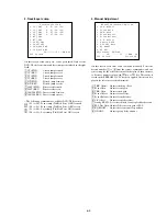
5. Auto Adjustment

On this screen, each item can be adjusted automatically. Select the
desired number 

[1]

 to 

[8]

 from the remote commander, and se-

lected item is adjusted automatically.

[1]

 Auto TRK. Offset:

Adjusts tracking offset.

[2]

 Auto Focus Balance: Adjusts focus balance.

[3]

 Auto Focus Offset:

Adjusts focus offset.

[4]

 Auto Focus Gain:

Adjusts focus gain.

[5]

 Auto TRK. Gain:

Adjusts track gain.

[6]

 Auto EQ

[7]

 Auto L.F. Offset:

Adjusts loop filter offset.

[8]

 Auto Group Delay

6. Memory Check

The display image is shown below and three screens in total can
be selected.

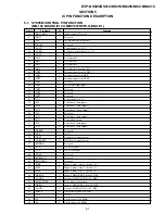
On this screen, current servo adjusted data stored in the EEPROM
are displayed. The adjusted data are initialized by pressing the

[CLEAR]

 key, but be careful that they are not recoverable after

initialization.
Before clearing the adjusted data, make a note of the set data. This
screen will also appear if [0] All is selected in the Drive Auto
Adjustment. In this case, default setting cannot be made.
“THR A&L” data on the second page cannot be changed if default
setting is once made.

Auto Adjustment

1. Auto TRK. Offset

2. Auto Focus Balance

3. Auto Focus Offset

4. Auto Focus Gain

5. Auto TRK. Gain

6. Auto EQ.

7. Auto L.F. Offset

8. Auto Group Delay

SA.04EF905 SI.00 EMG.00

DVD SL 12cm

EEPROM DATA 1

 

DL 

CD

LCD SL

L0

L1

Focus Gain

xx

xx

xx  xx

xx

TRK. Gain

xx

xx

xx

xx

xx

FCS Balnce

xx

xx

xx

xx

xx

Focus Bias

xx

xx

xx

xx

xx

TRV Offset

xx

xx

xx

xx

xx

L.F. Offset

xx

xx

xx

xx

xx

EQ. Boost

xx

xx

xx

xx

xx

_

UP

: Last Data

DOWN

: Next Data

CLEAR : Default Set

page.1/3

EEPROM DATA 2

 

DL 

CD

LCD SL

L0

L1

RF Jitter

xx

--

xx

xx

xx

RF Level

xx

--

xx

--

--

FE Level

xx

--

xx

--

--

FE Balance

xx

--

xx

--

--

TRV.Level

xx

--

xx

--

--

TE Gain

xx

xx

--

--

--

PI Level

xx

--

xx

xx

--

_

UP

: PREV Data

DOWN

: Next Data

CLEAR : Default Set

page.2/3

EEPROM DATA 3

 

DL 

CD

LCD SL

L0

L1

Analog FRSW

xx

xx

xx

xx

xx

PLL Dac Gain

xx

xx

xx

xx

xx

Mirror Time

xx

xx

xx

xx

xx

_  THR A&L

xx

xx

xx/xx xx

xx

UP

: PREV Data

DOWN

: First Data

CLEAR : Default Set

page.3/3

Summary of Contents for DVP-NS305

Page 1: ...uts Jack name Jack type Output or Input level Load impedance LINE IN AUDIO Phono jack 47 kilohms DVP NS315 NS415 DVP NS315 NS415 Outputs DVP NS305 NS310 NS405 NS410 LINE OUT AUDIO Phono jack 2 Vrms Over 10 kilohms DIGITAL OUT OPTICAL Optical output jack 18 dBm wave length 660 nm DIGITAL OUT COAXIAL Phono jack 0 5 Vp p 75 ohms COMPONENT VIDEO OUT Y PB PR Phono jack Y 1 0 Vp p PB PR 0 7 Vp p 75 ohms...

Page 2: ... the lead free mark LF indicating the solder contains no lead Caution Some printed circuit boards may not come printed with the lead free mark due to their particular size LEAD FREE MARK Unleaded solder has the following characteristics Unleaded solder melts at a temperature about 40 C higher than ordinary solder Ordinary soldering irons can be used but the iron tip has to be applied to the solder...

Page 3: ...play or Sound Track Language LANGUAGE SETUP 1 14 Settings for the Display SCREEN SETUP 1 14 Custom Settings CUSTOM SETUP 1 15 Settings for the Sound AUDIO SETUP 1 15 Additional Information 1 15 Troubleshooting 1 15 Self diagnosis Function When letters numbers appear in the display 1 16 Glossary 1 16 Language Code List 1 16 2 DISASSEMBLY 2 1 UPPER CASE 2 1 2 2 FRONT PANEL ASSEMBLY and FR SUPPORT 2 ...

Page 4: ...F CON SELF DIAGNOSTIC FUNCTION 6 12 6 11 TROUBLESHOOTING 6 19 7 ELECTRICAL ADJUSTMENT 7 1 POWER SUPPLY CHECK 7 1 1 SRV1246JUC Board 7 1 7 2 ADJUSTMENT OF VIDEO SYSTEM 7 2 1 Video Level Adjustment MB 103 BOARD 7 2 2 Checking S Video Output S Y 7 2 3 Checking S Video Output S C 7 2 4 Checking Component Video Output Y 7 2 5 Checking Component Video Output B Y 7 3 6 Checking Component Video Output R Y...

Page 5: ...e from the main unit Refer to 2 1 2 Remove the MB 103 board Refer to 2 7 3 Set the removed MB 103 board and CK 122 board to the stand as shown in Fig 2 Tray The lever of a zipper cam Hole B A CK 120 board J 6090 127 A CK 122 board J 6090 129 A FFC 26P J 6090 117 A FFC 9P J 6090 118 A FFC 5P J 6090 119 A FFC 15P J 6090 121 A FFC 25P J 6090 122 A Harness 6P J 6090 126 A Flexible flat cable five Stan...

Page 6: ...P 4 FMO 004 flexible board CN103 9P 5 MF 128 Harness CN109 6P 8 Connector CN111 9P 7 Connector CN113 25P 2 four screws SUMIEITE B3 BV 1 Flat cable FFC 26P CN203 3 Flat cable FFC 5P CN201 2 Flat cable FFC 9P CN204 8 Flat cable FFC 15P CN202 CK 121 board 6 Connector CN112 7 Connector CN102 5 Connector CN104 4 Connector CN106 1 Flat cable FFC 25P CN301 CK 122 board 3 Harness 6P CN102 4 Harness 6P CN1...

Page 7: ... 7 6 Set complete Fig 6 ...

Page 8: ... 8 MEMO ...

Page 9: ...of the unit and only will play DVD VIDEO discs playback only labeled with identical region codes This system is used to protect copyrights DVDs labeled will also play on this player If you try to play any other DVD the message Playback prohibited by area limitations will appear on the TV screen Depending on the DVD no region code indication may be labeled even though playing the DVD is prohibited ...

Page 10: ...acks 33 Playing status continued 10 Rear panel DVP NS315 DVP NS415 A DIGITAL OUT COAXIAL jack 22 23 24 B DIGITAL OUT OPTICAL jack DVP NS415 only 22 23 24 C LINE IN L R AUDIO jacks DVP NS415 only 16 18 D LINE IN VIDEO jack DVP NS415 only 16 18 E S VIDEO OUT jack 18 F COMPONENT VIDEO OUT jacks 18 G LINE OUT VIDEO jack 18 H LINE OUT L R AUDIO jacks 21 22 23 PCM DTS DOLBY DIGITAL COMPONENT VIDEO OUT C...

Page 11: ...aining time 41 m Display 4 DVD playback only O Format of the current audio signal 43 m No display m Return to Display 1 CHAPTER T41 8 T 1 01 57 DOLBY DIGITAL 3 2 1 continued 14 Displaying the Control Bar in stop mode The following displays appear when the DISPLAY button is repeatedly pressed during stop mode You can make basic adjustments and customize the player to suit your viewing preferences D...

Page 12: ...cator lights up in red With the playback side facing down 18 Hookups Hooking Up the Player Follow Steps 1 to 4 to hook up and adjust the settings of the player Before you start disconnect the power cords check that you have all of the supplied accessories and insert the batteries into the remote page 15 Notes Plug cords securely to prevent unwanted noise Refer to the instructions supplied with the...

Page 13: ... In this case you can also connect the player directly to the MD deck or DAT deck without using your stereo amplifier receiver Recommended surround sound effects for the connection only TVS STANDARD page 45 z Hint In connection you can use the supplied audio video cord instead of using a separate audio cord Note If you select one of the TVS effects page 44 while playing a disc no sound will come f...

Page 14: ...DTS is selected 12Press X x to select whether or not you wish to send a DTS signal to your amplifier receiver Choose the item that matches the audio connection you selected on pages 22 to 24 through OFF page 62 ON only if the amplifier receiver has a DTS decoder page 62 13Press ENTER Quick Setup is finished All connections and setup operations are complete Enjoying the surround sound effects To en...

Page 15: ...Search During playback turn and hold the Playback Dial clockwise to locate a point in the playback direction or counterclockwise to locate a point in the opposite direction When you find the point you want release the dial to return to normal playback speed Using the Multi mode Playback Dial on the player DVP NS415 only You can search for a particular point on a disc in various ways using the MODE...

Page 16: ...Ws However the discs must be recorded according to ISO9660 level 1 level 2 or Joliet format for the player to recognize the tracks You can also play discs recorded in Multi Session See the instructions of the CD R RW device or recording software not supplied for details on the recording format To play a Multi Session CD This player can play Multi Session CDs when an MP3 audio track is located in t...

Page 17: ...shuffling may produce a different playing order 1 Press DISPLAY during playback The following Control Bar appears 2 Press C c to select SHUFFLE then press ENTER repeatedly to select the item to be shuffled When playing a DVD TITLE CHAPTER When playing a VIDEO CD or CD TRACK When Program Play is activated ON shuffles titles chapters or tracks selected in Program Play To return to normal play Press ...

Page 18: ...TV screen also on the front panel display The information on the front panel display changes as follows when you DISPLAY ENTER TIME TEXT DVP NS315 DVP NS415 T41 8 T 1 01 57 Time information Title track CD VIDEO CD scene or album number Chapter index or track DATA CD BRAHMS SYMPHONY continued 42 change the time information on your TV screen When playing a DVD When playing a DATA CD MP3 audio When p...

Page 19: ...kers The virtual speakers are reproduced as shown in the illustration below Use this setting when you want to use TVS with 2 separate speakers z Hint You can also change the setting by pressing SUR or SURROUND on the player repeatedly Notes When the playing signal does not contain a signal for the rear speakers the surround effects will be difficult to hear When you select one of the TVS modes tur...

Page 20: ...can soften the images on the screen 1 Press DISPLAY twice during playback The following Control Bar appears 2 Press C c to select DIGITAL VIDEO ENHANCER then press ENTER repeatedly to select a level 1 enhances the outline 2 enhances the outline more than 1 3 enhances the outline more than 2 SOFT softens the image DVD only To cancel the DIGITAL VIDEO ENHANCER setting Select OFF in Step 2 To turn of...

Page 21: ...g X x to select the digit followed by C c to move the cursor then press ENTER You can also use the number buttons to enter your password DVP NS415 only The display for confirming the password appears When you have already registered a password The display for entering the password appears 4 Enter or re enter your 4 digit password by pressing X x to select the digit followed by C c to move the curs...

Page 22: ...picture on the TV screen in stop mode or while playing a CD or DATA CD MP3 audio 4 3 LETTER BOX Select this when you connect a 4 3 screen TV Displays a wide picture with bands on the upper and lower portions of the screen 4 3 PAN SCAN Select this when you connect a 4 3 screen TV Automatically displays the wide picture on the entire screen and cuts off the portions that do not fit 16 9 Select this ...

Page 23: ... Normally select this position When you select ON see Setting the digital output signal for further settings OFF The influence of the digital circuit upon the analog circuit is minimal continued 62 Setting the digital output signal Switches the method of outputting audio signals when you connect a component such as an amplifier receiver or MD deck with a digital input jack For connection details s...

Page 24: ...wegian 1393 Occitan 1403 Afan Oromo 1408 Oriya 1417 Punjabi 1428 Polish 1435 Pashto Pushto 1436 Portuguese 1463 Quechua 1481 Rhaeto Romance 1482 Kirundi 1483 Romanian 1489 Russian 1491 Kinyarwanda 1495 Sanskrit 1498 Sindhi 1501 Sangho 1502 Serbo Croatian 1503 Singhalese 1505 Slovak 1506 Slovenian 1507 Samoan 1508 Shona 1509 Somali 1511 Albanian 1512 Serbian 1513 Siswati 1514 Sesotho 1515 Sundanese...

Page 25: ...r given 2 1 UPPER CASE 2 2 FRONT PANEL ASSEMBLY and FR SUPPORT 2 Tapping screws 1 Tapping screws 7 Tray cover Chassis back 4 Upper case 5 6 3 Three screws SUMIEITE B3 BV 1 Claw 3 Two claws 6 Two claws 5 Front panel assmbly 4 Three claws 2 Claw 8 FL 126 board 7 Connector FF 206 CN301 3P 9 Two screws SUMIEITE B3 BV 0 FP support ...

Page 26: ...ible board CN203 26P 2 FMO 4 flexible board CN204 9P 1 FMS 17 flexible board CN201 6P 5 Loading assembly 4 Therr screws SUMIEITE B3 BV 2 FMO 4 flexible board 9P 3 FMM 41 flexible board 26P 4 Insulator 5 Two Insulator 1 Therr Insulator screws 6 Optical device KHM 270AAA ...

Page 27: ... 14R BOARD 7 Remove solder two places 9 FMS 17 flexible board CN001 5P 8 DC motor M001 0 MS 81 board 6 Pulley motor 5 Two screws P 2 6 3 1 Two claws 3 Tray 2 4 Belt 2 Two screws SUMIEITE B3 BV 3 ER 14R board 1 FAE 9 flexible board CN901 21P ...

Page 28: ...P 4 Two screws SUMIEITE B3 BV 3 Three screws SUMIEITE B3 BV 5 AV 61 board 6 FMM 41 flexible board CN203 26P 3 FMS 17 flexible board CN201 5P 5 FMO 4 flexible board CN204 9P 7 four screws SUMIEITE B3 BV 8 MB 103 board 4 Connector CN102 6P 2 Connector CN101 9P 1 Connector CN601 25P ...

Page 29: ...ible board CN201 5P 9 Two screws SUMIEITE B3 BV 0 IF 89 board 7 Connector PF 127 CN401 13P 7 Connector FF 206 CN406 3P 5 Connector CN402 7P 6 Connector CN102 6P 4 Connector CN101 9P 2 10 SWITCHING REGULATOR 3 Therr screws SUMIEITE B3 BV 1 Connector CN101 2P 1 Connector FF 127 CN201 13P 4 Power block ...

Page 30: ...2 6 2 11 INTERNAL VIEWS DC motor Loading DC motor Loading 1 763 790 11 Optical device KHM 270AAA Z NP A 6062 709 A ...

Page 31: ...OARDS LOCATION MB 103 board DVD CD RF AMP SERVO MOYOR DRIVE AD DECODER SYSTEM CONTROL AUDIO ADC PLL AV 61 board AUDIO VIDEO OUT IF 89 board IF COM FL 126 board LED MS 81 board LIADING MOTOR ER 14 board AV AMP Power block ...

Page 32: ...2 8E MEMO ...

Page 33: ...MOTOR SLED MOTOR M001 LOADING MOTOR FUNCTION KEY ND401 FLUORESCENT INDICATOR TUBE IF COM P CON POWER SERIAL BUS EEPROM PARALLEL BUS CDDOUT CDDATA CDBCK CDLRCK SDI 0 7 AV DECODER SPDIF ACH12 ACH34 ACH56 BCK LRCK 16M DRAM 16M SDRAM V Y C Y Cb Cr VIDEO BUFFER SPDIF IC204 AUDIO D A CONVERTER IC201 AUDIO AMP EVER 3 3V 11V 5V SW 3 3V 1 8V SW 3 3V 5V SW 11V EVER 13V INLIMIT SENSOR CHUCK TRAY DETECT SWITC...

Page 34: ...PO 163164 GIO9 FGREF GIO10 FGIN GIO1 INT3 PWM2 PWM0 1 POM 0 1 GIO0 INT2 SPINDLE MOTOR DRIVE FOCUS COIL DRIVE TRACKING COIL DRIVE LOADING MOTOR DRIVE SLED MOTOR DRIVE 7 1 ı 4 9 8 1 5 4 IC202 5 2 4 1 2 CN402 CN001 LDM CKSW1 OCSW1 INLIMIT SENSOR TRACKING COIL FOCUS COIL M001 LOADING MOTOR M M M M M M MS 81 BOARD SEE PAGE 4 17 SLED MOTOR SPINDLE MOTOR CN204 39 VCI 19 39 20 22 16 17 155 GIO2 INT4 16 CH...

Page 35: ... SDDQ 0 15 CDDATA CDBCK CDLRCK CDDOUT CLK CKE DQML DQMU CS WE CAS RAS WE RAS LCAS UCAS C OUT Y OUT COMPOUT B OUT R OUT G OUT C Y V Cr B Cb R Y G COUT YOUT COMPOUT CR B CB R Y G VIDEO SEE PAGE 3 9 AUDIO SEE PAGE 3 11 VREFI ACH12 ACH34 ACH56 LAND LRCKO BCKO ACH12 LRCK BCK VIDEO LEVEL ADJ RV401 HD 0 15 HAD 0 21 HA 0 21 HD 0 15 D 0 7 A 0 7 HA 0 7 HD 8 15 XRD XWRH RSTn DM ACK1 DM REQ1 DM ACK0 DM REQ0 A...

Page 36: ...16 5MHz XDRVMUTE INT2 WIDE CS5X CKSW1 XDRVMUTE XSDPIT OCSW1 XLDON XSDPCS CKSW1 DREQ0 INTO DACK0 CS2X CS3X DREQ1 DACK1 DREQ0 XAVDIT DACK0 XAVDCS2 XAVDCS3 DREQ1 DACK1 VIDEO SEE PAGE 3 9 SIGNAL PROCESSOR SEE PAGE 3 5 RF SERVO SEE PAGE 3 4 16 33MARP 512FSAVD X102 27MHz 33 1OUT FSEL 512FS6CH 512FS2CH TRST 29 SO1 SO1 30 SC1 SC1 79 XDACS XDACS INT1 CS4X XWAIT 35 XRST XRST XRST XRD XWRH 512 2OUT 512 1OUT ...

Page 37: ...CESSOR SEE PAGE 3 6 16 SYSTEM CONTROL SEE PAGE 3 8 INTERFACE CONTROL SEE PAGE 3 13 J104 2 2 J103 16 5 11 3 1 CN103 Y Cb Cr LINE3 LINE OUT VIDEO 1 VIDEO 2 Y C S VIDEO OUT VIDEO IN Y IN C IN MUTE1 Y IN Cb IN Cr IN MUTE2 VIDEO OUT Y OUT C OUT Y OUT Cb OUT Cr OUT V Y C Y Cb Cr Q104 105 WIDE SWITCH 1 24 D1 VIDEO OUT 1 IC102 ed 2 5Vp p H 2 IC102 ea 1 8Vp p H 3 IC102 wl 2 0Vp p H 4 IC102 wf 2 0Vp p H 5 I...

Page 38: ...SEE PAGE 3 13 ALT 16 J104 2 2 3 BICK 2 LRCK 4 MCLK 1 CSN 6 PDN 5 CCLK 7 CDTI 8 17 CN601 3 3 11 ALT 15 5 ART 21 3 ART 23 4 LMUTE 22 2 MAMUTE 24 MB 103 BOARD 4 4 SEE PAGE 4 27 AV 61 BOARD 2 2 SEE PAGE 4 33 10 IC204 OPTICAL DIGITAL OUT COAXIAL SPDIF J201 16 CN202 2 2 2 SPDIF 1 D IN ACH12 LRCK BCK SO1 SC1 XRST 512FS2CH XDACS MAMUTE D202 Q211 BUFFER Q208 MUTE Q207 MUTE 1 7 Q202 204 205 MUTE DRIVE L R A...

Page 39: ...SEE PAGE 3 9 IC404 IF CON IC405 RESET CN404 SC0 SI0 SO0 XIFBUSY XIFCS XFRRST SC SO SI BUSY CS FRRST 16 A MUTE VMUTE AMUTE VMUTE IR OUT PICTURE MODE SURRUND S406 S405 S404 S402 S408 POWER SEG 1 23 DIG 1 7 X401 8MHz ND401 FLUORESCENT INDICATOR TUBE CN401 POWER 1 IC406 REMOTE COMMANDER RECEIVER 2 1 CN402 SC0 SI0 SO0 XIFBUSY XIFCS XFRRST 34 PLAY 35 O C S401 S407 S403 36 TVS XIN XOUT 1 VOUT 8 RST SWITC...

Page 40: ...O COUPLER IC101 SWITCH 8 11 3 2 1 13 1 2 Q211 Q311 Q611 Q404 405 PS401 L102 LINE FILTER D221 P611 3 3V REG Q712 POWER CONTROL L211 L221 L311 L611 L512 26 37 IC404 IF CON IC406 REMOTE COMMANDER RECEIVER IC405 RESET IC412 IC611 SHUNT REG PCONT IC403 1 8V REG POWER 30 PONCHK VKK F2 F1 EVER 3 3V EVER 3 3V EVER 3 3V AI 5V 3 3V 5V 1 8V SW 11V 11V 3 3V MNT ND401 FLUORESCENT INDICATOR TUBE POWER SUPPLY AU...

Page 41: ...V REG 4 VOUT 5 VIN IC401 1 8V REG 4 VOUT 5 VIN IC302 3 3V REG 4 VOUT 5 VIN MUTE V SW 13V EVER 3 3V AU 11V D201 IC204 OPTICAL DIGITAL OUT CN203 25 CN601 POWER 1 SEE PAGE 3 16 POWER 1 SEE PAGE 3 16 IC201 AUDIO AMP Q201 Q203 216 OPTICAL DIGITAL OUT FILTER FL110 7 4 IC104 SYSTEM CONTROL FILTER FL103 FILTER FL201 3 3V FILTER FL105 2 5V FILTER FL104 1 1 8V FILTER FL109 5 CN202 6 5 7 3 11V 3 3V MNT IC303...

Page 42: ...3 20E MEMO ...

Page 43: ...DVD LD SLA H SLA SPM SLB MOD FMS 017 LED RF SPM E G FMO 004 F FCS VR TRK SLB FMM 041 GND 3 3V_MNT XIFCS XIFBUSY SO0 SI0 SC0 5V 3 3V M_GND 1 8V XFRRST GND 11V GND LDM OCSW1 LDM CKSW1 GND VR GND FCS VC TRK SW N C RF A N C H G FCS F CD LD N C VCC E N C B PD D C TRK DVD LD GND MOD LD GND SPM SLA INLIM SLA SPM SLB GND LED SLB MAMUTE ART ALT GND DISCEXT RGBSEL ART 25P RMUTE SPDIF Y G C GND P_GND_2CH WID...

Page 44: ...10 W un less otherwise specified kΩ 1000Ω MΩ 1000kΩ Caution when replacing chip parts New parts must be attached after removal of chip Be careful not to heat the minus side of tantalum capacitor be cause it is damaged by the heat All variable and adjustable resistors have characteristic curve B unless otherwise noted 2 non flammable resistor 5 fusible resistor C panel designation f internal compon...

Page 45: ... CN202 4 DVD PLAY 1 9Vp p 40ms div 8 CN202 4 CD PLAY 1 8Vp p 200ms div qs IC403 ws 4 8Vp p 40 8nsec 9 IC301 zb 4 6Vp p 30nsec q IC301 zzz CL301 DVD PLAY 1 2Vp p 40ns div qa IC301 zzc CL302 CD PLAY 1 4Vp p 0 2µs div qd IC403 tg H 950mVp p w IC601 1 40 8nsec 5 2Vp p qj IC403 yd 850mVp p H qg IC403 tl 650mVp p H qk IC403 yg 1 1Vp p H qh IC403 ya 650mVp p H 950mVp p H qf IC403 tj ql IC403 zb zn 5 1Vp ...

Page 46: ... B 6 Q404 D 7 Q405 D 8 S401 A 1 S402 A 2 S403 A 2 S404 A 4 S405 A 2 S406 A 4 S407 A 2 S408 A 8 For printed wiring board There are a few cases that the part printed on this diagram isn t mounted in this model MB 103 board DVD CD RF AMP SERVO MOTOR DRIVE AD DECODER SYSTEM CONTROL AUDIO ADC PLL AV 61 board AUDIO VIDEO OUT IF 89 board IF COM FL 126 board LED MS 81 board LOADING MOTOR ER 14 board AV AM...

Page 47: ...ED PORT JL415 10k R426 2 2 R459 0 01u C426 0 1u C427 10k R460 0 1u B C428 3P CN301 1 5V 2 N C 3 LED PORT D301 EB3804X TP 220 R301 1 A SEG16 SEG15 SEG20 SEG19 SEG18 SEG17 SEG14 SEG13 SEG6 SEG7 SEG8 SEG9 SEG12 SEG11 SEG10 DIG3 DIG2 DIG1 SEG21 SEG22 DIG4 DIG5 DIG6 DIG7 SEG1 SEG2 SEG3 SEG4 SEG5 DIG7 DIG6 DIG5 DIG4 DIG3 DIG2 DIG1 SEG1 SEG2 SEG3 SEG4 SEG5 SEG6 SEG7 SEG8 SEG9 SEG10 SEG11 SEG12 SEG13 SEG1...

Page 48: ... A CN101 A 3 CN102 A 1 CN103 A 4 CN201 A 2 CN203 C 1 CN204 B 1 CN601 D 1 IC104 B 4 IC301 A 2 IC302 B 2 IC402 D 5 IC403 C 4 IC601 D 3 RV401 D 4 For printed wiring board There are a few cases that the part printed on this diagram isn t mounted in this model Uses unleaded solder MB 103 board DVD CD RF AMP SERVO MOTOR DRIVE AD DECODER SYSTEM CONTROL AUDIO ADC PLL AV 61 board AUDIO VIDEO OUT IF 89 boar...

Page 49: ...4 13 DVD CD RF AMP DIGITAL SERVO MOTOR DRIVE SERVO AV DECODER SDRAM SYSTEM CONTROL AUDIO DAC PLL MB 103 MB 103 BOARD SIDE B IC101 A 1 IC103 B 3 IC106 B 1 IC201 C 4 IC202 B 4 IC303 A 3 IC401 B 2 IC404 C 2 Q201 C 5 Q202 D 5 Uses unleaded solder ...

Page 50: ... 5 6 7 8 9 INLIM TRK FCS FCS SVC TRK SVC 1 A SPM SLA SLB SPM SLB SLA SSCS B SSDFCTI H SSWD F TE SSDFCTI D DVD_LD FE G SLA H FCS SLB TRK A B FCS CD_LD D DVD_LD SSCS G PI SSCK MIRR SPM C C SPM TRK E SLA FE CD_LD PI SLB TE FE SSCK SSWD SSRD TZC E F SSRD A MIRR TZC TE PI INLIM SLA SLB SLB SPM SLA SPM FCS FCS TRK TRK INLIM CDPD N C DVDPD RFIN MEVO CDLD MIRR VPA DVD LD RF TZIN F GND E MB SLA MEV AIP RFI...

Page 51: ...6k R223 220k R242 SLDB 100p C225 MDPO 100 R207 330 R262 0 1u B C273 XX R280 TSENSD CL201 CL202 CL203 CL204 CL205 XX R271 XX R274 XX R270 XX C276 TSENSO XX C223 XX R257 XX C274 XX R276 XX R275 XX R258 XX C231 XX C222 5P 1 2 3 4 5 CN201 5P 1 2 3 4 5 6 7 8 9 10 11 FCS FCS TRK TRK 1 A SLA SLB SLA SPM SPM SLB CKSW1 SPM LDM LDM FCS TRK FCS OCSW1 SPM SLA SLB TRK CKSW1 LDM OCSW1 LDM SLB SLA TRK TRK FCS SP...

Page 52: ...MA3 RAMA2 RAMA1 RAMA0 MDPO SDEF XSAK XSHD SDCK CDDOUT SSCS LMM LMP SSCK SSWD SSRD CDBCK EMU0 CDDATA EMU1 SDEF XSAK XSRQ XSHD SDCK CDDOUT SDI0 SDI1 SDI2 SDI3 SDI4 SDI5 SDI6 SDI7 MDSO TESTK3 TESTK2 TESTK1 TESTK0 TESTK3 TESTK2 TESTK1 TESTK0 XSDPIT XSDPCS XSDPCS FDRV FDRV TDRV TDRV MDPO MDSO FDRV FDRV TDRV TDRV XSDPIT SLE SPFG RAMD0 RAMD1 RAMD2 RAMD3 RAMD4 RAMD5 RAMD6 RAMD7 RAMD8 RAMD9 RAMD10 RAMD11 R...

Page 53: ...VD6 DVD5 DVD4 DVD3 DVD2 DVD1 DVD0 HA1 HA2 HA3 HA4 HA5 HA6 HA7 HA8 HA9 HA10 HA11 HA12 HA13 HA14 HA15 HA16 HA17 HA18 HA19 HA20 HA21 HD0 HD1 HD2 HD3 HD4 HD5 HD6 HD7 HD8 HD9 HD10 HD11 HD12 HD13 HD14 HD15 SDI0 SDI1 SDI2 SDI3 SDI4 SDI5 SDI6 SDI7 DVD0 DVD1 DVD2 DVD3 DVD4 DVD5 DVD6 DVD7 HA0 SDAD11O CVD07 HAD14I CVD03 SDDQ4 SDDQ1 DT5I DO ACH56O IVALIn HAD18I IOVSS07 DVO4 TDI CVD01 DVSS33 HAD22I SDRASOn COU...

Page 54: ...T7 ADAD7 ADAD10 ADDT0 ADAD8 ADDT1 ADAD9 ADDT14 ADDT8 ADDT4 ADDT13 ADDT10 ADDT0 ADDT9 ADDT11 ADAD3 ADAD2 ADAD1 ADAD0 ADAD10 ADDT7 ADDT6 ADDT5 ADDT4 ADDT3 ADDT2 ADDT1 ADDT0 ADAD4 ADAD5 ADAD6 ADAD7 ADAD8 ADAD9 ADDT8 ADDT9 ADDT10 ADDT11 ADDT12 ADDT13 ADDT14 ADDT15 ADAD11 ADDT0 ADDT15 ADDT1 ADDT14 ADDT2 ADDT13 ADDT3 ADDT12 ADDT14 ADDT11 ADDT5 ADDT10 ADDT6 ADDT9 ADDT7 ADDT8 ADAD11 ADAD9 ADAD10 ADAD8 ADA...

Page 55: ...15 HA11 HA3 HA13 HD6 HD6 HA3 HD9 HD3 HD1 HA11 HD5 HD2 HA16 HD14 HD0 HA8 HA13 HA2 HA19 SI2 SO2 SI0 SO0 SC0 XSDPIT XARPIT XAVDIT IPSW RGBSEL TRMP EUROVY EXT DSEL FSEL HA21 HA20 HA19 HA18 HA17 HA16 HA15 HA14 HA13 HA12 HA11 HA10 HA9 HA8 HA7 HA6 HA5 HA4 HA3 HA2 HA1 HA0 OCSW2 WIDE TRMM XWAIT XDACS HD8 HD9 HD10 HD11 HD12 HD13 HD14 HD15 HD7 HD6 HD5 HD4 HD3 HD2 HD1 HD0 IPSW WIDE RGBSEL EUROVY EXT DSEL DACK...

Page 56: ...186 JL119 33MAVD 6P CN102 1 2 3 4 5 6 FL109 X102 FB106 0uH XX R158 2 2 R108 XX C119 27MAVD JL114 JL122 100 R183 CN101 9P 1 2 3 4 5 6 7 8 9 11V 0 R159 4 7uH L101 FL101 100 R182 JL106 XX C112 6P CN103 1 2 3 4 5 6 1k R185 RFMON JL123 JL124 JL125 JL126 JL129 FSEL XIFBUSY SI2 SI0 SC0 XIFCS XFRRST SO0 SO2 1 8V 3 3V GND 3 3V GND GND 3 3V 1 8V GND 3 3V 5V GND 3 3V 5V 5V 3 3V GND 1 A SO0 SC0 SI0 SO2 SI0 SI...

Page 57: ...C407 B 6 Q404 D 7 Q405 D 8 S401 A 1 S402 A 2 S403 A 2 S404 A 4 S405 A 2 S406 A 4 S407 A 2 S408 A 8 For printed wiring board There are a few cases that the part printed on this diagram isn t mounted in this model Uses unleaded solder MB 103 board DVD CD RF AMP SERVO MOTOR DRIVE AD DECODER SYSTEM CONTROL AUDIO ADC PLL AV 61 board AUDIO VIDEO OUT IF 89 board IF COM FL 126 board LED MS 81 board LOADIN...

Page 58: ...p CH C201 2200 R207 560p CH C202 470 R241 4700 0 5 R203 100k R218 7P CN202 1 2 3 4 5 6 7 V 5600 0 5 R205 JL223 JL204 JL237 D_GND_VIDEO JL235 VMUTE 16V 47u C227 ERAUDIOL 180p CH C205 470 R226 4700 0 5 R202 1k R254 470 R220 D_GND_VIDEO JL207 DAN202K T 146 D201 XX C218 JL234 JL222 CB R 10k R228 C216 XX 0 01u B C208 JL211 XX C241 68 R251 2SC2712 YG TE85L Q203 JL215 R242 470 R243 470 XX R287 XX C226 16...

Page 59: ...123 JL110 HZM6 8ZWA1TL D105 10k R129 JL136 AU 11V 0 01u B C101 XX R124 SW_ 13V 0 1u B C114 JL112 IC102 LA73050 TLM NC 1 NC 2 VIDEO_IN 3 DCCNT1 4 GND 5 C_IN 6 MUTE1 7 Y_IN 8 NC DCCNT2 9 NC GND 10 NC 11 Y_IN NC 12 DCCNT2 13 GND 14 Cb_IN 15 MUTE2 16 Cr_IN 17 5V 18 5V 19 CB_OUT 22 GND 23 Y_OUT 24 5V NC 25 NC 26 5V 27 5V 28 Y_OUT 29 NC 30 C_OUT 31 GND 32 VIDEO_OUT 33 5V 34 NC 35 NC 36 NC 21 Cr_OUT 20 H...

Page 60: ...oard There are a few cases that the part printed on this diagram isn t mounted in this model Uses unleaded solder MB 103 board DVD CD RF AMP SERVO MOTOR DRIVE AD DECODER SYSTEM CONTROL AUDIO ADC PLL AV 61 board AUDIO VIDEO OUT IF 89 board IF COM FL 126 board LED MS 81 board LOADING MOTOR ER 14 board AV AMP Power block ...

Page 61: ...1 N C 12 GND E 13 GND E 14 R C_OUT 15 BLANKING_OUT 16 GND E 17 GND E 18 V Y_OUT 19 V_IN 20 GND E 21 XX R941 JL950 2200 R914 R958 0uH JL949 330 R911 JL947 47k R905 JL944 100p C962 68 R929 JL934 JL935 470 R924 100uH L905 FB908 0uH XX R940 XX R901 2SD601A QRS TX Q902 2200 R917 HZM6 8ZWA1TL D919 1k R915 UN2111 TX Q907 JL938 XX R919 JL925 JL941 UN2213 TX Q906 JL928 330 R912 R957 0uH JL924 JL917 JL931 1...

Page 62: ...GULATOR POWER BLOCK HS11S1 HS11S1F POWER BOARD SW REG HS11S1 1 468 645 11 POWER BOARD SW REG HS11S1F 1 468 647 11 MB 103 board DVD CD RF AMP SERVO MOTOR DRIVE AD DECODER SYSTEM CONTROL AUDIO ADC PLL AV 61 board AUDIO VIDEO OUT IF 89 board IF COM FL 126 board LED MS 81 board LOADING MOTOR ER 14 board AV AMP Power block ...

Page 63: ...50V IC101 M1P2E4 L110 45 C151 100p HS11S1F 150p HS11S1U 2kV C110 150u 400V L150 SHORT D S C Z150 ST02D 170 T101 TR010032 HS11S1F TR011019 HS11S1U POWER TRANSFORMER D211 D2L20U D213 D1NS4 6 D221 D1NL20U D312 D1N60 D311 D1NS4 D611 D1NS4 P611 2 0A 125V C221 100u35V L311 39uH L611 10uH C311 150u 35V C611 330u 35V P311 1A 125V C223 47u 35V C213 47u 35V L221 100uH C211 150u 35V L211 10u R212 47k Q211 2S...

Page 64: ...DVP NS305 NS310 NS315 NS405 NS410 NS415 4 44E MEMO ...

Page 65: ... Power supply 3 3 V Reference power supply 3 3 V GND Set of mode 0 Set of mode 1 Set of mode 2 Set of mode 3 fixed at H Interrupt input from AV DEC Interrupt input from ARP Interrupt input from SDSP Not used IF CON interrupt input Not used Not used Not used Power supply 3 3 V Serial bus 0 data input Serial bus 0 data output Serial bus 0 clock output Not used Serial bus 1 data output Serial clock o...

Page 66: ...M Not used Chip select signal output for AV DEC Chip select signal output for AV DEC Chip select signal output for ARP Chip select signal output for SERVO DSP Power supply 1 8 V Not used Not used Wait signal input Test terminal fixed at H Test terminal fixed at L Read timing signal output High order byte write timing signal output Not used Fixed at H Power supply 1 8 V GND Reset signal input from ...

Page 67: ...quest from SYSTEM CONTROL 02 Power Off by Emergency Power Off Command from SYSTEM CONTROL if information is sent from SYSTEM CONTROL 03 IF CON Judged that SYSTEM CONTROL is Faulty 04 Power Off from Diagnosis Mode of IF CON 05 Forced Power Off by the User 06 Power Off by Power Supply Voltage Monitor 0 Quit Quit the Syscon Diagnosis and return to the Test Mode Menu 1 All items continuous check This ...

Page 68: ...played Error Not detected The model code read from the EEPROM is displayed with 2 digit hexadecimal number 2 5 Region Region code is displayed Error Not detected The region code determined from the model code is dis played 2 6 M t Check Mount resistance is checked Error 22 The region code does not accord Check whether the region code that is deduced from model resistance and destination resistance...

Page 69: ...y in case of an error is different from the display of other diagnosis described later Before starting the test all addresses of RAM IC303 are cleared to 0x0000 First 0xA55A is written to the address 0x00000 and the address data are read and checked from addresses 0x00001 to 0x80000 while shifting 1 bit each Next the data at that address is cleared and it is written to the address 0x00001 and read...

Page 70: ... the color bar sig nals are output This check is performed for European model only 7 6 Component Out European model only Component video output check AVD color bar command write tVideo Component OUT Error Not detected With the component of video output turned on the color bar signals are output This check is performed for European model only 7 7 Euro AV Through European model only AV Through outpu...

Page 71: ...displayed Normally 0 is selected to adjust DVD single layer CD and DVD dual layer in this order But individual items can be ad justed for the case where adjustment is suspended due to an error In this mode the adjustment can be made easily through the op eration following the message displayed on the screen Which disc is currently adjusted is displayed on the fluorescent display tube 0 ALL You wil...

Page 72: ... 5 LD ON 6 Focus Error Check 7 Fcs ON 1 with PI Level measure 8 Auto Track Offset Adjust L0 9 Trv Level Check 10 Tracking ON 11 CLVA ON 12 Sled ON 13 Auto Focus Balance Adjust 14 Auto Loop Filter Offset Adjust 15 Auto Focus Gain Adjust L0 16 Auto Focus Balance Adjust L0 17 Eq Boost Adjust 18 Auto Loop Filter Offset Adjust 19 Auto Track Gain Adjust 20 Copy Adjustment Data to LCD 21 RF Level Measure...

Page 73: ...k Memory On this screen the mirror time is measured and written to the EEPROM to check the disc type First set a DVD SL disc and press 1 then set a CD disc and press 2 and finally set a DVD DL disc and press 3 The measured mirror time is displayed re spectively The adjustment must be executed more than once after default data were written From this screen you can go to another mode by pressing or ...

Page 74: ...ot locked The spindle could run overriding the control if the spindle system is faulty or RF is not present In such a case do not operate CLVA 0 Reset SLED TILT Reset the Sled and Tilt to initial position Reset the Sled only to initial position be cause the Tilt mechanism is not available in this model 1 LD Turn ON OFF the laser 2 SP Turn ON OFF the spindle 3 Focus Search the focus and turn on the...

Page 75: ...and cur rent setting for the selected item will be displayed then increase or decrease numeric value with key or 4 key This value is stored in the EEPROM If CLV has been applied the jitter is dis played for reference for the adjustment 1 TRK Offset Adjusts tracking offset 2 Focus Gain Adjusts focus gain 3 TRK Gain Adjusts track gain 4 Focus Offset Adjusts focus offset 5 Focus Balance Adjusts focus...

Page 76: ... if 0 All is selected in the Drive Auto Adjustment In this case default setting cannot be made THRA L data on the second page cannot be changed if default setting is once made Auto Adjustment 1 Auto TRK Offset 2 Auto Focus Balance 3 Auto Focus Offset 4 Auto Focus Gain 5 Auto TRK Gain 6 Auto EQ 7 Auto L F Offset 8 Auto Group Delay SA 04EF905 SI 00 EMG 00 DVD SL 12cm EEPROM DATA 1 DL CD LCD SL L0 L1...

Page 77: ...CLEAR keys in this order The data have been initialized when Set Up Initialized mes sage is displayed The EMG History display screen will be restored soon 6 8 VERSION INFORMATION The ROM version region code OPT type etc are displayed if 5 is selected in the Test Mode Menu The parenthesized hexadeci mal number in the version number field indicates the checksum value of the ROM Note after Downloadin...

Page 78: ...ation monitoring display of fluo rescent display tube and LED control 1 The routine that monitors 3 3 V PCONT of MB 103 board is not provided 2 The monitoring timer for serial communication with the SYS TEM CONTROL is not provided The main unit is not placed in the Standby mode even if the communication with SYS TEM CONTROL is normal 3 Display of fluorescent display tube Normally display is made f...

Page 79: ...eck mode becomes active at the AC Power ON or by key input the test display of the following steps 1 to 4 is repeated 1 FLD and LED all ON for 5 seconds 2 MODEL display for 2 seconds 3 Version display for 2 seconds 4 ROM creation date display for 2 seconds ...

Page 80: ...Mode Keys on the main unit except keys transited in Self Check Mode 2 3 2 2 Operation and Display When a key on the main unit is pressed in the Self Check mode the name of that key is displayed on the FLD Also the key name display and the key code display can be switched with the DISPLAY key on the remote commander NOTHING is displayed when nothing is entered Also VIDEO CD DVD and CD segments turn...

Page 81: ...commander keys except keys transited in Self Check Mode 2 3 3 2 Operation and Display When a key on the remote commander is pressed in the Self Check Mode the name of that key is displayed on the FLD Also the key name display and the key code display can be switched with the DISPLAY key on the remote commander NOTHING is displayed when nothing is entered Also VIDEO CD DVD and CD segments turn on w...

Page 82: ...TLE and therefore use another DVD remote commander having the JOG SHUTTLE 2 3 5 2 Operation and Display The Self Check Mode transits to this mode when 5 key is en tered This tests whether each segment turns on individually Only the first segment of each grid of FLD turns on and each time the SHUTTLE is entered the segment of each grid is switched in or der When SHUTTLE input is clockwise the segme...

Page 83: ...HUTTLE is entered the grid is switched in order When SHUTTLE input is clock wise the grid switches in 1 2 3 direction or counterclockwise it switches in 3 2 1 direction Display at the start of Grid Test r Input in CW direction 2 3 7 LED Test Display 2 3 7 1 Transition Keys in Self Check Mode 4 key on the remote commander SHUTTLE on the remote commander during Grid Test display This model does not ...

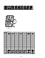
Page 84: ... P13 P14 P15 P16 P17 P18 P19 P20 a h j k b f m s g e n p r c d Dp a h j k b f m s g e n p r c d Dp a h j k b f m s g e n p r c d Dp a h j k b f m s g e n p r c d Dp a h j k b f m s g e n p r c d Dp a h j k b f m s g e n p r c d Dp a h j k b f m s g e n p r c d ANODE CONNECTION 7G 1G 1G 7G 6G 5G 4G 3G 2G 1G 2G ...

Page 85: ...hat each IC is working normally 1 3 Clock signal check Measure the clock signal frequency at CPUCK CL101 of SYSCON IC104 with an oscilloscope If the 8 25 MHz signal appears t Check the machine ac cording to section 1 3 1 If the 33 MHz signal appears t Check the machine accord ing to section 1 3 2 If other frequencies are output R110 and R113 have defective soldering X101 crystal os cillator is def...

Page 86: ...heck the CS signal that is currently output The CS signal other than CS0X is being output t IC mount is defective or the IC is defective depending on the moving CS signal CS2X CS3X AVD IC403 CS4X CS5X ARP SERVO IC301 If the trouble is not applicable to any of the above phenomenon SYSCON IC104 or ROM IC106 or IC107 is defective 3 If the message SDSP No Ack appears after the menu is displayed 3 1 AR...

Page 87: ...ressed 3 1 Check CN201 voltage of the power supply block when the LED lights in green If voltage is abnormal t The power supply block is defec tive or the IF 89 board is defective or MB103 is defective 3 2 Check XFRRST pin 8 at CN101 on the MB 103 board If it is fixed to L t The signal line has defective solder ing or is short circuited with other signal lines or parts are defective 3 3 Check IFBS...

Page 88: ...6 22E MEMO ...

Page 89: ...505 J 6090 089 A dual layer 7 SACD reference disc HLXA 509 J 6090 090 A 8 Extension Cable J 6090 107 A 7 1 POWER SUPPLY CHECK 1 SRV1246JUC Board Mode E E Instrument Digital voltmeter EVER 3 3 V Check Test point CN201 pin qa Specification 3 5 0 2 Vdc SW 3 3 V Check Test point CN201 pin 8 Specification 3 3 0 2 Vdc 5 V Check Test point CN201 pin qs Specification 5 0 0 3 Vdc SW 11 V Check Test point C...

Page 90: ...t set so that color bars are generated 2 Confirm that the S Y level is 1 0 0 05 Vp p Fig 7 2 3 Checking S Video Output S C Purpose This checks whether the S video output S C satisfies the NTSC standard If it is not correct the colors will be too dark or too light Mode Video level adjustment in test mode Signal Color bars Test point S VIDEO OUT S C connector 75 Ω terminated Instrument Oscilloscope ...

Page 91: ... set so that color bars are generated 2 Confirm that the B Y level is 700 50 mVp p Fig 7 5 6 Checking Component Video Output R Y Purpose This checks component video output R Y If it is incorrect correct color will not be displayed when connected to for instance component input projector Mode Video level adjustment in test mode Signal Color bars Test point COMPONENT VIDEO OUT CR connector D1 VIDEO ...

Page 92: ...7 4E 7 3 ADJUSTMENT RELATED PARTS ARRANGEMENT MB 103 BOARD Side A SRV1246JUC BOARD Side A RV401 IC403 VIDEO LEVEL ADJ CN201 13 1 ...

Page 93: ...equired for routine service Some delay should be anticipated when ordering these items The mechanical parts with no reference number in the exploded views are not supplied The components identified by mark 0or dotted line with mark 0 are critical for safety Replace only with part number specified Les composants identifiés par une marque 0 sont critiques pour la sécurité Ne les remplacer que par un...

Page 94: ...8 2 1 2 ns ns ns mechanism deck section a b c c e e 3 4 5 5 5 5 5 ns 13 12 14 15 6 19 20 16 17 21 22 18 ns a f f b 5 ns ns 10 11 14 12 8 1 1 MAIN SECTION ns not supplied ...

Page 95: ...EP1 AEP2 UK RU ME2 EA ME5 HK SP NS310 NS315 PX E AR NS405 NS410 NS415 ME5 011 1 757 140 11 CORD POWER NS305 ME2 EA ME5 SP NS315 PX E AR BR NS415 ME5 011 1 757 571 11 CORD POWER NS315 US CND NS415 US CND 011 1 782 752 31 CORD POWER NS305 KR 011 1 783 531 11 CORD POWER NS315 MX 011 1 783 531 31 CORD POWER NS315 US CND MX NS415 US CND 011 1 790 390 41 CORD POWER NS305 TW 011 1 790 588 11 CORD POWER N...

Page 96: ...8 4 52 60 a a ns ns ns M001 CN001 ns ns 53 61 54 55 55 55 56 57 58 S001 8 1 2 MECHANISM DECK SECTION ns not supplied ...

Page 97: ...7 1 823 829 11 FMO 4 FLEXIBLE FLAT CABLE 58 1 823 828 11 FMM 41 FLEXIBLE FLAT CABLE 59 60 3 053 841 01 PULLEY GEAR 60 3 053 841 21 GEAR PULLEY 61 4 974 711 01 SCREW 2X5 P TYIGHT PTTWH M001 1 763 790 11 MOTOR DC LOADING S001 1 786 133 11 SWITCH ROTARY CN001 1 815 412 11 CONNECTOR FFC FPC 5P 3 058 511 51 BV IBR NS315 US4 Ref No Part No Description Remarks Ref No Part No Description Remarks ...

Page 98: ... CHIP 560PF 5 50V C203 1 163 257 11 CERAMIC CHIP 180PF 5 50V C204 1 163 257 11 CERAMIC CHIP 180PF 5 50V C205 1 163 257 11 CERAMIC CHIP 180PF 5 50V C206 1 163 257 11 CERAMIC CHIP 180PF 5 50V C207 1 162 970 11 CERAMIC CHIP 0 01uF 10 25V C208 1 162 970 11 CERAMIC CHIP 0 01uF 10 25V C209 1 126 960 11 ELECT 1uF 20 50V C210 1 126 947 11 ELECT 47uF 20 16V C211 1 126 947 11 ELECT 47uF 20 16V C212 1 126 96...

Page 99: ... AUS HK SP TW KR NS315 NS405 NS410 NS415 R122 1 216 049 11 RES CHIP 1K 5 1 10W NS305 AEP1 AEP2 UK RU NS310 NS405 NS410 R126 1 216 021 00 METAL CHIP 68 5 1 10W NS305 ME2 EA ME5 AUS HK SP TW KR NS315 NS415 R127 1 216 021 00 METAL CHIP 68 5 1 10W NS305 ME2 EA ME5 AUS HK SP TW KR NS315 NS415 R128 1 216 021 00 METAL CHIP 68 5 1 10W NS305 ME2 EA ME5 AUS HK SP TW KR NS315 NS415 R129 1 216 073 91 RES CHIP...

Page 100: ...127 715 91 CERAMIC CHIP 0 22uF 10 16V C943 1 162 927 11 CERAMIC CHIP 100PF 5 50V C945 1 162 927 11 CERAMIC CHIP 100PF 5 50V C962 1 162 927 11 CERAMIC CHIP 100PF 5 50V C963 1 162 927 11 CERAMIC CHIP 100PF 5 50V CONNECTOR CN901 1 815 387 11 CONNECTOR FPC FFC 21P DIODE D901 8 719 073 01 DIODE MA111 K8 S0 D907 8 719 050 37 DIODE M1MA152WA T1 D917 8 719 067 40 DIODE STZ6 8N T146 D918 8 719 067 40 DIODE...

Page 101: ... 10 25V C420 1 162 970 11 CERAMIC CHIP 0 01uF 10 25V C421 1 128 551 11 ELECT 22uF 20 25V C423 1 162 970 11 CERAMIC CHIP 0 01uF 10 25V C424 1 107 826 11 CERAMIC CHIP 0 1uF 10 16V C425 1 128 551 11 ELECT 22uF 20 25V C426 1 163 021 91 CERAMIC CHIP 0 01uF 10 50V C427 1 107 826 11 CERAMIC CHIP 0 1uF 10 16V C428 1 107 826 11 CERAMIC CHIP 0 1uF 10 16V CONNECTOR CN401 1 506 478 11 PIN CONNECTOR 13P CN405 ...

Page 102: ...05 AEP1 AEP2 UK NS410 NS415 R418 1 216 027 00 METAL CHIP 120 5 1 10W NS305 NS310 NS315 NS405 AEP1 AEP2 UK NS410 NS415 R424 1 216 073 91 RES CHIP 10K 5 1 10W NS305 NS310 NS315 NS405 AEP1 AEP2 UK NS410 NS415 R425 1 216 073 91 RES CHIP 10K 5 1 10W NS305 NS310 NS315 NS405 AEP1 AEP2 UK NS410 NS415 R426 1 216 073 91 RES CHIP 10K 5 1 10W NS305 NS310 NS315 NS405 AEP1 AEP2 UK NS410 NS415 R428 1 216 025 11 ...

Page 103: ...HIP 0 01uF 10 25V C122 1 162 970 11 CERAMIC CHIP 0 01uF 10 25V C125 1 126 607 11 ELECT CHIP 47uF 20 4V C126 1 126 206 11 ELECT CHIP 100uF 20 6 3V C127 1 126 204 11 ELECT CHIP 47uF 20 16V C128 1 126 246 11 ELECT CHIP 220uF 20 4V C129 1 162 970 11 CERAMIC CHIP 0 01uF 10 25V C201 1 162 970 11 CERAMIC CHIP 0 01uF 10 25V C202 1 162 970 11 CERAMIC CHIP 0 01uF 10 25V C203 1 162 964 11 CERAMIC CHIP 0 001u...

Page 104: ... 162 970 11 CERAMIC CHIP 0 01uF 10 25V C338 1 162 970 11 CERAMIC CHIP 0 01uF 10 25V C339 1 162 970 11 CERAMIC CHIP 0 01uF 10 25V C340 1 162 970 11 CERAMIC CHIP 0 01uF 10 25V C343 1 162 970 11 CERAMIC CHIP 0 01uF 10 25V C344 1 162 970 11 CERAMIC CHIP 0 01uF 10 25V C401 1 124 779 00 ELECT CHIP 10uF 20 16V C402 1 124 779 00 ELECT CHIP 10uF 20 16V C403 1 162 970 11 CERAMIC CHIP 0 01uF 10 25V C404 1 12...

Page 105: ...6W R104 1 216 809 11 METAL CHIP 100 5 1 16W R105 1 216 809 11 METAL CHIP 100 5 1 16W R106 1 216 809 11 METAL CHIP 100 5 1 16W R108 1 216 789 11 METAL CHIP 2 2 5 1 16W R110 1 216 821 11 METAL CHIP 1K 5 1 16W R111 1 216 809 11 METAL CHIP 100 5 1 16W R112 1 216 809 11 METAL CHIP 100 5 1 16W R113 1 216 837 11 METAL CHIP 22K 5 1 16W R114 1 216 821 11 METAL CHIP 1K 5 1 16W NS305 AEP1 AEP2 UK RU NS310 NS...

Page 106: ...1 216 853 11 METAL CHIP 470K 5 1 16W R244 1 216 821 11 METAL CHIP 1K 5 1 16W R245 1 216 841 11 METAL CHIP 47K 5 1 16W R246 1 216 809 11 METAL CHIP 100 5 1 16W R248 1 216 803 11 METAL CHIP 33 5 1 16W R249 1 216 803 11 METAL CHIP 33 5 1 16W R250 1 218 895 11 METAL CHIP 100K 0 5 1 10W R251 1 216 841 11 METAL CHIP 47K 5 1 16W R252 1 216 839 11 METAL CHIP 33K 5 1 16W R253 1 218 889 11 METAL CHIP 56K 0 ...

Page 107: ...R FFC FPC 5P SWITCH S001 1 786 133 11 SWITCH ROTARY MISCELLANEOUS 4 1 468 645 11 POWER BLOCK NS305 TW NS315 US CND MX NS415 US CND 4 1 468 646 11 POWER BLOCK NS305 ME2 EA ME5 AUS HK SP KR NS315 AR NS415 ME5 AUS 4 1 468 647 11 POWER BLOCK NS315 PX E BR 4 1 468 648 11 POWER BLOCK NS305 AEP AEP2 UK RU NS310 NS405 NS410 011 1 575 651 21 CORD POWER NS305 AEP1 AEP2 UK RU ME2 EA ME5 HK SP NS310 NS315 PX ...

Page 108: ...DVP NS305 NS310 NS315 NS405 NS410 NS415 140 Sony Corporation Home Video Company 9 929 717 11 2002C1600 1 2002 3 Published by Quality Assurance Dept ...

Reviews: