


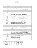


– 15 –
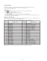
Pin No.
Pin Name
I/O
Function
36
MODEL.SEL2
I
Destination setting terminal (fixed at “L”)
37
AVSS
—
Ground terminal (for A/D converter)
38
RST
I
System reset signal input from the reset signal generator (IC930) “L”: reset
For several hundreds msec. after the power supply rises, “L” is input, then it changes to “H”
39
EXTAL
I
Main system clock input terminal (8 MHz)
40
XTAL
O
Main system clock output terminal (8 MHz)
41
VSS
—
Ground terminal
42
TX
O
Sub system clock output terminal Not used (open)
43
TEX
I
Sub system clock input terminal Not used (fixed at “L”)
44
VDD (+5V)
—
Power supply terminal (+5V)
45
VFDP (–30V)
—
Power supply terminal (–30V) (for FL drive)
46
XSEL
O
Not used (open)
47
REINIT
O
Not used (open)
48
RFGF
O
Laser power hold control signal output to the CXA2568M (IC103) “H”: hold on
49 to 66
OPEN
O
Not used (open)
67 to 87
S21 to S1
O
Segment drive signal output to the fluorescent indicator tube (FL801) “H”: goes on
88
1G
O
Grid drive signal output to the fluorescent indicator tube (FL801) “H”: goes on
89
VDD (+5V)
—
Power supply terminal (+5V)
90 to 100
2G to 12G
O
Grid drive signal output to the fluorescent indicator tube (FL801) “H”: goes on


