


– 14 –
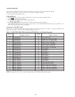
6-1.
IC PIN FUNCTION DESCRIPTION
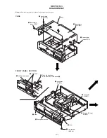
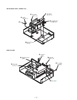
SECTION 6
DIAGRAMS
•
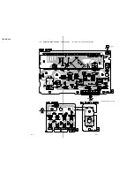
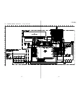
DISP BOARD IC801 CXP82832-009Q (SYSTEM CONTROLLER/FL DRIVER)
Pin No.
Pin Name
I/O
Function
1, 2
13G, 14G
O
Grid drive signal output to the fluorescent indicator tube (FL801) “H”: goes on
3
NC
—
Not used (fixed at “H”)
4
+5V
—
Power supply terminal (+5V)
5
SCOR
I
Subcode sync (S0+S1) detection signal input from the CXD2585Q (IC101) in BD section
“H” active
6, 7
GND
—
Ground terminal
8
RMIN
I
Sircs signal input from the remote control receiver (IC802) “L” active
9
GND
—
Ground terminal
10, 11
OPEN
O
Not used (open)
12
LDOUT
O
Motor control signal (load out direction) output to the loading motor driver (IC302)
“H” active *1
13
LDIN
O
Motor control signal (load in direction) output to the loading motor driver (IC302)
“H” active *1
14
SENSE
I
Internal status monitor input from the CXD2585Q (IC101) in BD section
15
XLT
O
Serial data latch pulse output to the CXD2585Q (IC101) in BD section “L” active
16
DMUTE
O
Digital muting on/off control signal output to the CXD2585Q (IC101) and D/A converter (IC301)
“L”: muting on
17
PRGLT
O
Serial data latch pulse output to the D/A converter (IC301) “L” active
18
SENSOR IN
I
Stabilizer detect sensor input terminal (fixed at “L” in this set)
19
BUSOUT
O
Sircs remote control signal output for the CONTROL A1 “H” active
20
BUSIN
I
Sircs remote control signal input for the CONTROL A1 “L” active
21
SENSOR SW
I
Stabilizer detect sensor switch input terminal “H” active Not used (open)
22
CLK
O
Serial data transfer clock signal output to the CXD2585Q (IC101) in BD section “L” active
23
LDON
O
Laser on/off control signal output to the CXA2568M (IC103) “H”: laser on
24
DATA
O
Serial data output to the CXD2585Q (IC101) in BD section
25
SQCK
O
Subcode Q data reading clock signal output to the CXD2585Q (IC101) in BD section
“L” active
26
SUBQ
I
Subcode Q data input from the CXD2585Q (IC101) in BD section
27
+5V
—
Power supply terminal (+5V)
28
AVREF
I
Reference voltage (+5V) input terminal (for A/D converter)
29
KEY0
I
Key input terminal (A/D input) S851 to S858 (LANGUAGE, MUSIC SCAN, AUTO SPACE,
PEAK SEARCH, PLAY MODE, REPEAT, FADER, TIME/TEXT keys input)
30
KEY1
I
Key input terminal (A/D input) S801 to S805 and S810 (CLEAR, CHECK, EDIT/TIME FADE,
0
,
)
, PUSH ENTER keys input)
31
KEY2
I
Key input terminal (A/D input)
S806 to S810 (
§
OPEN/CLOSE,
·
,
P
,
p
,
≠
AMS
±
keys input)
32
FILTER.SW
I
FILTER switch (S860) input terminal (A/D input)
33
ADJ/AFADJ
I
Input terminal for the CD test mode setting
“L”: ADJ mode, center voltage: AFADJ mode, normally: “H”
34
LOADSW
I
Loading in/out detect switch (S152 and S153) input terminal
35
MODEL.SEL1
I
Destination setting terminal (fixed at “H”)
*1 Loading motor (M903) control
IN
OUT
BRAKE
RUN IDLE
LDOUT (pin
!™
)
“L”
“H”
“H”
“L”
LDIN (pin
!£
)
“H”
“L”
“H”
“L”
Operation
Terminal


