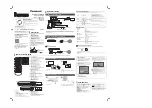
background image

CDP-S3

8

3-4.

MAIN  BOARD

3-5.

FRONT  PANEL  SECTION

2

connector
(CN401)

1

wire (flat type) (21 core)
(CN301)

2

two connectors
(CN101, 102)

5

MAIN board

3

screw
(BVTP3 

×

 8)

4

lug

3

screw
(BVTP3 

×

 8)

2

connector
(CN701)

3

two screws
(BVTP3 

×

 8)

2

three screws
(BVTP3 

×

 8)

3

two claws

1

connector
(CN401)

4

front panel section

3

claw

Summary of Contents for CDP-S3

Page 1: ...ystem Compact disc and digital audio system Laser Semiconductor laser λ 780 nm Emission duration continuous Frequency response 2 Hz 20 kHz 0 5 dB Signal to noise ratio More than 90 dB Dynamic range More than 90 dB OPTICAL OUT Square optical connector jack rear panel Dimensions w h d Approx 280 x 108 x 330 mm Mass Approx 2 7 kg Design and specifications are subject to change without notice 9 873 83...

Page 2: ... diode emis sion observe from more than 30 cm away from the objective lens LASER DIODE AND FOCUS SEARCH OPERATION CHECK Carry out the S curve check in CD section adjustment and check that the S curve waveforms is output three times Notes on chip component replacement Never reuse a disconnected chip component Notice that the minus side of a tantalum capacitor may be dam aged by heat Flexible Circui...

Page 3: ...rinted Wiring Board BD Section 14 6 3 Schematic Diagram BD Section 15 6 4 Printed Wiring Boards CD CHANGER Section 16 6 5 Schematic Diagram CD CHANGER Section 17 6 6 Printed Wiring Board MAIN Section 18 6 7 Schematic Diagram MAIN Section 19 6 8 Printed Wiring Boards PANEL Section 20 6 9 Schematic Diagram PANEL Section 21 6 10 IC Pin Function Description 24 7 EXPLODED VIEWS 7 1 General Section 26 7...

Page 4: ...he disc table with the test disc label facing up and chuck the disc 2 Press the CD button to set CD function and press the n N button to playback the disc 3 The following will be displayed on the liquid crystal display Display 1KHZ 0DB L R 4 Pressing the or button select the track The text data of each track will be displayed For details of the displayed contents for each track refer to Table 1 CD...

Page 5: ... forward ea 14 x hH H hH O o P p M m X 1 2 3 wg qh qa wk wj wh wa 4 5 6 7 qs qf qd qg 8 9 q qk ql w qj wd ws wf es ea e wl CD H es 14 15 CHECK 5 15 CLEAR 6 15 CLOCK TIMER SELECT qj 30 CLOCK TIMER SET qk 13 21 29 DBFB qg 23 DISPLAY ws 13 16 18 29 35 D SKIP 4 14 ENTER wg 10 12 13 15 17 18 21 22 26 30 EQ qd 27 EQ ON OFF qf 10 28 FUNCTION wf 10 14 15 20 21 31 GROOVE wa 23 SET UP qs 10 12 26 28 29 SLEE...

Page 6: ...n the order shown below 3 1 DISASSEMBLY FLOW SECTION 3 DISASSEMBLY 3 2 COVER Page 7 3 3 CD MECHANISM DECK CDM63B 30BD60 Page 7 3 6 PANEL L BOARD PANEL R BOARD Page 9 3 7 LID CD Page 9 3 5 FRONT PANEL SECTION Page 8 3 4 MAIN BOARD Page 8 SET ...

Page 7: ...e Follow the disassembly procedure in the numerical order given 3 2 COVER 1 two screws case 3 TP2 3 cover 2 screw BVTT3 6 1 two screws case 3 TP2 3 four screws BVTP3 8 1 wire flat type 21 core CN301 2 connector CN701 4 CD mechanism deck CDM63B 30BD60 ...

Page 8: ... 2 connector CN401 1 wire flat type 21 core CN301 2 two connectors CN101 102 5 MAIN board 3 screw BVTP3 8 4 lug 3 screw BVTP3 8 2 connector CN701 3 two screws BVTP3 8 2 three screws BVTP3 8 3 two claws 1 connector CN401 4 front panel section 3 claw ...

Page 9: ... 9 3 6 PANEL L BOARD PANEL R BOARD 3 7 LID CD 5 two claws 4 four screws BVTP2 6 8 6 PANEL R board 1 five screws BVTP2 6 8 3 PANEL L board 2 two claws 3 lid CD 4 spring CD 1 screw BVTP2 6 8 2 bracket LID assy ...

Page 10: ...Mode Procedure 1 Enter the GC test mode 2 Press the DISC 2 or TUNING 2 button to set the key check mode and displays K 0 J 0 V 0 on the fluorescent indicator tube of tuner unit 3 All buttons are pressed of CD unit all LEDs are blinking of CD unit not change the display of fluorescent indicator tube Releasing the GC Test Mode To release from this mode press three buttons in the same manner as enter...

Page 11: ...rm RF Level Check Procedure 1 Connect an oscilloscope CH1 to TP RFDC and CH2 to TP RFAC 2 Turn Power switch on 3 Load a disc LUV P01 and playback 4 Confirm that oscilloscope waveform is clear and check if RF signal level is correct or not Note Clear RF signal waveform means that the shape can be clearly distinguished at the center of the waveform BD board Oscilloscope TP FEO TP DVC symmetry S curv...

Page 12: ...ors are in Ω and 1 4 W or less unless otherwise specified f internal component C panel designation A B Line Voltages are taken with a VOM Input impedance 10 MΩ Voltage variations may be noted due to normal produc tion tolerances Waveforms are taken with a oscilloscope Voltage variations may be noted due to normal produc tion tolerances Circled numbers refer to waveforms Signal path J CD PLAY Note ...

Page 13: ...13 CDP S3 Circuit Boards Location DISC SENSOR board BD board IN OUT SW board MOTOR board DRIVER board TRAY SENSOR board MAIN board PANEL L board PANEL R board ...

Page 14: ...tion There are a few cases that the part printed on this diagram isn t mounted in this model Semiconductor Location Ref No Location MAIN BOARD CN301 M102 SLED TP RFDC TP RFAC TP FEI TP DVC TP TEO TP FEO M101 SPINDLE A D101 B 3 IC101 C 3 IC102 B 2 IC103 D 2 Q101 C 1 Q102 A 3 Page 18 ...

Page 15: ...IAGRAM BD Section See page 22 for Waveforms See page 22 for IC Block Diagrams Voltages and waveforms are dc with respect to ground under no signal conditions no mark CD PLAY Note The components identified by mark 0 or dotted line with mark 0 are critical for safety Replace only with part number specified Page 19 ...

Page 16: ... S3 16 16 6 4 PRINTED WIRING BOARDS CD CHANGER Section See page 13 for Circuit Boards Location MAIN BOARD NO202 1 5 There are a few cases that the part isn t mounted in model is printed on diagrams Page 18 ...

Page 17: ...age 22 for IC Block Diagram Voltages and waveforms are dc with respect to ground under no signal conditions no mark CD STOP B MAIN BOARD NO202 IC731 SUB TRAY1 HEIGHT SENSOR IC732 SUB TRAY2 HEIGHT SENSOR IC733 SUB TRAY3 HEIGHT SENSOR IC751 DISC IN DETECT Page 19 ...

Page 18: ...39 CD303 JW142 D515 R424 R429 R430 R442 C425 C427 R493 JW159 R456 R441 R443 R490 R438 R496 R445 R449 R450 R446 R447 R452 R500 R453 JW147 R473 R469 R465 R477 R481 JW148 JW111 R444 JW169 R494 R482 R491 R489 R132 R133 R134 L125 R492 JW162 JW165 JW135 JW170 R412 JW136 CD301 CD311 CD312 JW134 JW172 R459 R457 JW161 NO202 JW102 D105 VCD101 JW99 JW116 JW98 C301 JW175 JW177 JW150 C521 JW176 C125 JW140 CLP1...

Page 19: ... 100 2 2k 10k 16MHz 330 10 50V 100 10k 1 50V 100 0 022 10 50V BA1A4M RT1P137S MTZA 2 2A 11ES2 0 1 100 470 10V 100k 100 100 100 100 100 100 100 150 10k 10k 4 7k 100 100 100 10k 0 022 0 022 0 022 100 100 100 9P 150 150 150 150 150 TA7807S 1SS133 10k 21P SN74HCT04ANS E05 TOTX140 M30620MAA B31FP 100 100 100 1 1 0 1 0 1 0 1 220 10V 12P JW 84 85 86 87 24 33 35 37 40 42 43 44 45 46 47 48 49 26 28 12 29 3...

Page 20: ... D704 D705 NO702 R713 R711 R712 R714 R715 R716 NO703 R710 S708 S707 S706 S705 S704 S703 S702 S701 NO701 R701 R702 R703 R704 R705 R706 R707 R700 C MAIN BOARD CN401 1 9 PANEL L BOARD PANEL R BOARD 1 680 995 11 21 1 680 996 11 21 1 2 1 2 M x X N m D701 S716 D702 S717 3 2 1 Z DISC 3 Z DISC 3 DISC 2 DISC 1 PLAY MODE REPEAT DISC 2 Z DISC 1 Page 18 ...

Page 21: ... R716 R707 R706 R705 R704 R703 R702 R701 R700 S702 S701 S703 S704 S705 S706 S707 S708 CNW703 CN702 CN701 S711 S712 S714 S713 S715 S716 S717 SEL5923A SEL5423E SEL5923A SEL5923A SEL5923A 270 330 470 560 680 1k 1 2k 1 8k 1 2k 1k 680 560 470 330 270 9P 2P 2P DISC 3 DISC 1 DISC 2 DISC 1 DISC 3 DISC 2 REPEAT PLAY MODE ...

Page 22: ...K VDD SCOR SPOB XLON XTAI XVDD EMPH AVDD1 AOUT1 AIN1 XTAO XVSS AIN2 AOUT2 AVDD2 RMUT LOUT2 LOUT1 BCK LRCK PCMD LMUT AVSS1 AVSS2 CPU INTERFACE SERVO AUTO SEQUENCER SERIAL IN INTERFACE OVER SAMPLING DIGITAL FILTER 3rd ORDER NOISE SHAPER PWM PWM EFM DEMODULATOR TIMING LOGIC DIGITAL OUT D A INTERFACE DIGITAL PLL ASYMMETRY CORRECTOR CLOCK GENERATOR MIRR DFCT FOK DETECTOR DIGITAL CLV SUBCODE PROCESSOR S...

Page 23: ...M VC DVC 30 29 28 DVC VCC DVC 27 26 25 24 RW ROM EQ 23 22 21 20 19 RFAC VCA VCC DVC RW ROM VC RW ROM DVC 3 A B C D B C A A A B C D B C D D 1 2 APC AMP 5 6 7 8 9 4 RFAC SUMMING AMP RW ROM APC OFF Hi Z RW ROM H L VOFST VC RW ROM 10 11 GM GM 18 17 16 B D A C 13 14 15 12 EQ IN LD PD GND A B C D AC SUM E F DVCC DVC RFAC SW DC OFST RFDCI RFDCO VC RFC VFC BST RFG VCC CEI CE TE BAL TE FEI FE ...

Page 24: ...ner system ST S3 S5 31 Not used 32 SQ DATA IN I Subcode Q data input from the CXD3017Q IC101 33 SQ CLK O Subcode Q data reading clock signal output to the CXD3017Q IC101 34 RTS1 Not used 35 CD DATA O CD decode data output to the CXD3017Q IC101 36 SENS I Internal status SENSE signal input from the CXD3017Q IC101 37 CD CLK O Serial data transfer clock signal output to the CXD3017Q IC101 38 CD POWER ...

Page 25: ... indicator D702 L LED on 81 to 83 LED_PAUSE O LED drive signal output of the X indicator D701 L LED on 84 EXP IN DATA I Serial data input from the tape deck unit TC S3 85 EXP OUT DATA O Serial data output to the tape deck unit TC S3 86 EXP LAT O Serial data latch pulse signal output to the tape deck unit TC S3 87 EXP CLK O Serial data transfer clock signal output to the tape deck unit TC S3 88 LED...

Page 26: ... Color Ref No Part No Description Remark Ref No Part No Description Remark 1 X 4953 613 1 PANEL ASSY FRONT 2 4 233 136 01 LID CD 3 4 233 147 01 SPRING CD 4 4 951 620 01 SCREW 2 6X8 BVTP 5 1 680 996 11 PANEL R BOARD 6 1 680 995 11 PANEL L BOARD 7 3 363 099 21 SCREW CASE 3 TP2 8 4 233 134 11 COVER 9 1 823 055 11 WIRE FLAT TYPE 21 CORE 10 A 4725 658 A MAIN BOARD COMPLETE 11 1 757 633 11 CORD WITH CON...

Page 27: ...28 963 01 SLIDER STOCKER L 511 4 228 964 01 SLIDER STOCKER R 512 4 228 970 02 TRAY SUB 513 4 229 001 01 HOLDER SENSOR 514 4 228 975 02 COVER TRAY L 515 4 228 978 02 COVER TRAY R 516 4 228 970 12 TRAY SUB 517 4 228 970 22 TRAY SUB 518 X 4953 307 1 PULLEY A ASSY CHUCKING 519 4 234 423 01 SPRING STOCKER L LEAF 520 1 678 457 11 TRAY SENSOR BOARD 501 501 502 504 not supplied not supplied not supplied n...

Page 28: ...228 997 02 GEAR CAM 566 1 678 460 11 DRIVER BOARD 567 4 228 968 01 BELT 568 4 228 998 01 GEAR DETECTION 569 4 228 976 01 SLIDER BU R 570 1 678 461 11 MOTOR BOARD 571 X 4952 971 2 MOTOR ASSY 572 4 228 999 02 LEVER MAIN L 573 4 229 000 02 LEVER MAIN R 574 4 227 899 01 SCREW DIA 12 FLOATING 575 4 229 003 01 PULLEY 576 4 228 988 01 CHASSIS 577 4 218 253 61 SCREW M2 6 BTTP 578 4 218 253 71 SCREW M2 6 B...

Page 29: ...04 4 233 831 01 GEAR LA 605 1 757 710 11 WIRE FLAT TYPE 16 CORE 0606 A 4735 188 A BU 30 60 ASSY 5 7 627 853 28 SCREW PRECISION P 2X3 TYPE3 7 4 BASE UNIT SECTION BU 30BD60 The components identified by mark 0 or dotted line with mark 0 are critical for safety Replace only with part number specified not supplied not supplied 605 602 601 604 603 not supplied 5 5 606 ...

Page 30: ...uF 25V C126 1 163 038 11 CERAMIC CHIP 0 1uF 25V C127 1 124 584 00 ELECT 100uF 20 10V C129 1 162 974 11 CERAMIC CHIP 0 01uF 50V C130 1 163 038 11 CERAMIC CHIP 0 1uF 25V C131 1 104 665 11 ELECT 100uF 20 10V C133 1 162 921 11 CERAMIC CHIP 33PF 5 50V C143 1 163 038 11 CERAMIC CHIP 0 1uF 25V C145 1 163 038 11 CERAMIC CHIP 0 1uF 25V C153 1 163 038 11 CERAMIC CHIP 0 1uF 25V C159 1 162 970 11 CERAMIC CHIP...

Page 31: ...5 1 10W R190 1 216 033 00 METAL CHIP 220 5 1 10W R191 1 216 085 00 METAL CHIP 33K 5 1 10W R192 1 216 085 00 METAL CHIP 33K 5 1 10W R193 1 216 099 00 METAL CHIP 120K 5 1 10W R194 1 216 097 11 RES CHIP 100K 5 1 10W R195 1 216 113 00 METAL CHIP 470K 5 1 10W R196 1 216 057 00 METAL CHIP 2 2K 5 1 10W R198 1 216 295 11 SHORT 0 COMPOSITION CIRCUIT BLOCK RN101 1 233 576 11 RES CHIP NETWORK 100 VARIABLE RE...

Page 32: ...159 11 CERAMIC 0 1uF 50V C125 1 126 923 11 ELECT 220uF 20 10V C251 1 161 494 00 CERAMIC 0 022uF 25V C255 1 161 494 00 CERAMIC 0 022uF 25V C260 1 161 494 00 CERAMIC 0 022uF 25V C261 1 161 494 00 CERAMIC 0 022uF 25V C301 1 126 959 11 ELECT 0 47uF 20 50V C302 1 162 600 11 CERAMIC 0 0047uF 20 16V C303 1 162 306 11 CERAMIC 0 01uF 20 16V C304 1 161 494 00 CERAMIC 0 022uF 25V C310 1 161 494 00 CERAMIC 0 ...

Page 33: ...00 5 1 4W R496 1 249 429 11 CARBON 10K 5 1 4W R497 1 247 807 31 CARBON 100 5 1 4W R500 1 249 429 11 CARBON 10K 5 1 4W VIBRATOR X401 1 781 107 21 VIBRATOR CERAMIC 16MHz 1 678 461 11 MOTOR BOARD CAPACITOR C721 1 162 306 11 CERAMIC 0 01uF 30 16V 1 680 995 11 PANEL L BOARD LED D701 8 719 057 97 LED SEL5923A TP15 X D702 8 719 058 03 LED SEL5423E TP15 N D703 8 719 057 97 LED SEL5923A TP15 3 D704 8 719 0...

Page 34: ...7 876 11 CARBON 75K 5 1 4W R734 1 249 408 11 CARBON 180 5 1 4W R735 1 247 876 11 CARBON 75K 5 1 4W R736 1 249 408 11 CARBON 180 5 1 4W MISCELLANEOUS 9 1 823 055 11 WIRE FLAT TYPE 21 CORE 11 1 757 633 11 CORD WITH CONNECTOR 17P 571 X 4952 971 2 MOTOR ASSY 605 1 757 710 11 WIRE FLAT TYPE 16 CORE 0606 A 4735 188 A BU 30 60 ASSY M721 1 541 632 12 MOTOR DC LOADING The components identified by mark 0 or...

Page 35: ...35 CDP S3 MEMO ...

Page 36: ...ORY Clicking the version allows you to jump to the revised page Also clicking the version at the upper right on the revised page allows you to jump to the next revised page Ver Date Description of Revision 1 0 2001 04 New ...

Reviews: