Sony Corporation
Video Business Group
SERVICE MANUAL
9-890-708-11
2009D0500-1
© 2009.4
Published by Quality Assurance Dept.
BLU-RAY DISC/DVD PLAYER
BDP-BX2/S360
RMT-B104A/B105A
SPECIFICATIONS
US Model
Canadian Model
BDP-BX2/S360
PX Model
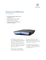
BDP-S360
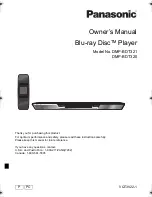
Photo: BDP-S360
TM
System
Laser:
Semiconductor laser
Inputs and outputs
(
Jack name:
Jack type/Output level/Load impedance)
LINE OUT R-AUDIO-L:
Phono jack/2 Vrms/10 kilohms
DIGITAL OUT (OPTICAL):
Optical output jack/–18 dBm
(wave length 660 nm)
DIGITAL OUT (COAXIAL):
Phono jack/0.5 Vp-p/75 ohms
HDMI OUT:
HDMI 19-pin standard connector
COMPONENT VIDEO OUT
Phono jack/Y: 1.0 Vp-p/
P
: 0.7 Vp-p/75 ohms
Phono jack/1.0 Vp-p/75 ohms
100BASE-TX Terminal
External memory slot (For connecting the
external memory)
DC output: 5 V 500 mA Max
General
Power requirements:
120 V AC, 60 Hz (US, Canadian)
110 – 240 V AC, 50/60 Hz (PX)
Power consumption:
22 W
Dimensions (approx.):
430 mm × 216 mm × 56 mm
(17 in. × 8
5
/
8
in. × 2
1
/
4
in.)
(width/depth/height) incl. projecting parts
Mass (approx.):
2.1 kg (4 lb 10
1
/
8
oz)
Operating temperature:
5 ºC to 35 ºC (41 °F to 95 °F)
Operating humidity:
25 % to 80 %
Supplied accessories
Specifications and design are subject to
change without notice.
• Audio/video cable (phono plug ×3) (1)
• AC power cord (1)
• HDMI cable (1) (BX2)
• Remote commander (remote) (1)
• Size AA (R6) batteries (2)
• Plug Adaptor (1) (PX)
www. xiaoyu163. com
QQ 376315150
9
9
2
8
9
4
2
9
8
TEL 13942296513
9
9
2
8
9
4
2
9
8
0
5
1
5
1
3
6
7
3
Q
Q
TEL 13942296513 QQ 376315150 892498299
TEL 13942296513 QQ 376315150 892498299