background image

32

AM-NX1

Rewriting the NV values

Caution: The application that meets the microcomputer version in this set must be used when rewriting the NV values. Rewriting the NV

values using the application not suitable for the microcomputer version could cause the set to malfunction.
For a checking method of the microcomputer version, see “SECTION 4 TEST MODE” (page 12).

Preparation

1. USB cable (attached to the set)
2. Personal computer in which the Net MD Driver has been installed. (For further information, see “System requirements” (page 4) in

“SECTION 1 SERVICING NOTES”)

3. Application “NVWriter” for NV values rewriting

How to get the application “NVWriter” for NV values rewriting

Contact our service technical support section for PA products to get the application.

Pre-check

1. Check the microcomputer version in this set. (For a checking method of the microcomputer version, see “SECTION 4 TEST MODE”

(page 12).)

2. Check that the Net MD Driver has been installed in the personal computer.
3. Make sure that the set is in the Normal mode.

Note:

 Do not rewrite the NV values in the Test mode.

Rewriting the NV values

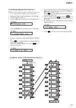
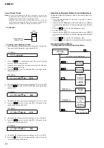
1. Connect the set to the personal computer with the USB cable.
2. Start the application “NVWriter”.
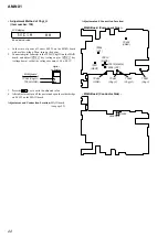
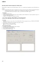
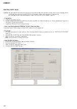
3. Make sure that the following window opens.
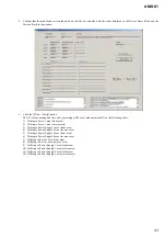
4. Click the [USB CONNECT] button.

Summary of Contents for AM-NX1

Page 1: ...lar Mechanism MZ N910 Mechanism Type MT MZN910 181 Optical Pick up Name ABX 1R Audio playing system MiniDisc digital audio system Laser diode properties Material GaAlAs Wavelength λ 790 nm Emission duration continuous Laser output less than 44 6 W This output is the value measured at a distance of 200 mm from the lens surface on the optical pick up block with 7 mm aperture Recording and playback t...

Page 2: ... Keep the temperature of the soldering iron around 270 C dur ing repairing Do not touch the soldering iron on the same conductor of the circuit board within 3 times Be careful not to apply force on the conductor when soldering or unsoldering UNLEADED SOLDER Boards requiring use of unleaded solder are printed with the lead free mark LF indicating the solder contains no lead Caution Some printed cir...

Page 3: ...Assy 11 4 TEST MODE 12 5 ELECTRICAL ADJUSTMENTS 17 6 DIAGRAMS 6 1 Block Diagram MAIN Section 37 6 2 Block Diagram POWER SUPPLY Section 38 6 3 Note for Printed Wiring Board and Schematic Diagrams 39 6 4 Printed Wiring Board MAIN Board Component Side 40 6 5 Printed Wiring Board MAIN Board Conductor Side 41 6 6 Schematic Diagram MAIN Board 1 4 42 6 7 Schematic Diagram MAIN Board 2 4 43 6 8 Schematic ...

Page 4: ... UNIT The laser diode in the optical pick up block may suffer electro static break down because of the potential difference generated by the charged electrostatic load etc on clothing and the human body During repair pay attention to electrostatic break down and also use the procedure in the printed matter which is included in the repair parts The flexible board is easily damaged and should be han...

Page 5: ...control A Volume control VOL Turn to adjust the volume B x stop button C NX ENTER button play pause enter D Display window E group F FF REW G Clip H HOLD switch Slide the switch in the direction of the arrow a yellow mark appears to disable the buttons on the remote control To prevent the buttons from being accidentally operated when you carry the recorder use this function I SOUND button J DISPLA...

Page 6: ...3 6 MECHANISM DECK SECTION MT MZN910 181 CASE BATTERY BLOCK Page 9 3 7 GEAR BSA GEAR SB Page 9 3 8 OP SERVICE ASSY ABX 1R Page 10 3 9 DC MOTOR SSM21A C NP SLED M702 DC MOTOR SSM18D C NP SPINDLE M701 DC MOTOR UNIT OVER WRITE HEAD UP DOWN M703 Page 10 3 10 HOLDER ASSY Page 11 SET Note 1 The process described in can be performed in any order Note 2 Without completing the process described in the next...

Page 7: ...e Follow the disassembly procedure in the numerical order given 3 2 BOTTOM CE PANEL SUB ASSY 3 3 MAIN BOARD 5 flexible board CN701 1 sheet radiation B 6 flexible board CN501 4 Remove two solders of flexible board from OP service assy 2 Remove the solder of terminal board minus 3 Remove the solder of battery terminal plus assy 7 three toothed lock screws M1 4 8 main board ...

Page 8: ... A and remove two bosses B 2 Open to the direction of the arrow C and remove two bosses D and convex part E 3 Open to the direction of the arrow F and remove two bosses G and convex part H 4 three convex parts 5 ornamental belt assy Note As the ornamental belt assy is very fragile do not give an excessive force to the entire assy when removing it convex part H boss G F convex part E boss D C A A b...

Page 9: ...GEAR BSA GEAR SB 2 convex part 3 convex part 9 escutcheon B 7 spring R 6 case battery block 5 four claws 0 set chassis assy 8 spring L 1 two step screws MD 4 mechanism deck section MT MZN910 181 1 self tap screw 2 thrust retainer spring 3 washer 0 8 2 5 4 gear BSA 5 gear SB ...

Page 10: ...lock assy 4 OP service assy ABX 1R 2 rack spring 1 precision pan screw M1 4 EG 3 two precision pan screws M1 4 EG 4 DC motor SSM21A C NP spindle M702 1 Remove four solders of flexible board 2 Remove two solders of flexible board 6 three self tap screws 7 DC motor SSM18D C NP spindle M701 8 washer 5 motor base assy 0 DC motor unit over write head up down 9 self tap screw ...

Page 11: ...AM NX1 11 3 10 HOLDER ASSY 4 Remove the holder assy to the direction of the arrow A 3 Open the holder assy 1 boss 2 boss A ...

Page 12: ...he remote commander is shown Setting Method of Test Mode Short SL803 TEST on the MAIN board with a solder bridge connect pin zx of IC801 to the ground Then turn on the power Note If electrical adjustment CD and MO overall adjustment has not been finished completely ERROR is displayed on LCD of the set SL803 TEST MAIN Board Conductor Side Operation in Setting the Test Mode When the test mode become...

Page 13: ...Display Mode Key Check Mode Test Mode Display Check Mode Press the x key Press the x key Press the x key Press the x key Press the or VOL key Press the key Press the VOL key Electrical Offset Adjustment Power Supply Adjustment Auto Item Feed CD Overall Adjustment MO Overall Adjustment Self Diagnosis Result Display Mode Press the DISPLAY key Press the DISPLAY key The key check quits or open the upp...

Page 14: ...ror occurred during the recording or playing the mechanism control block and the power supply control block in the micro computer detect it and record its cause as history in the nonvola tile memory By checking this history in the test mode you can analyze a fault and determine its location Total recording time is recorded as a guideline of how long the optical pick up has been used and by compari...

Page 15: ...TOC address error Tadr TOC address data error Power supply system error 22 Low battery LBat Momentary interruption detected 31 Offset error Ofst Offset error 32 Focus error ABCD ABCD Focus error ABCD offset error offset error Offset system error 33 Tracking error TE Tracking error Offset error Offset error 34 X1 tracking error X1TE X1 tracking error Offset error Offset error 35 MD DATA 2 MD2 MD DA...

Page 16: ...sult display mode and to return to the test mode display check mode press the x key LCD display P R 000 Total count of play system errors hex Total count of record system errors hex 0 00 P R 0 00 E I B 0 00 S t a t 0 00 A d r s 0 00 B E m p 0 00 P R Total play record errors hex Counter of sound skip check each item hex 6 digit address where sound was skipped last hex Playing sound skip result disp...

Page 17: ...lay the LCD on the remote commander is shown Precautions for Adjustment 1 Adjustment must be done in the test mode only After adjusting release the test mode 2 Use the following tools and measuring instruments Test CD disc TDYS 1 Part No 4 963 646 01 SONY MO disc available on the market Digital voltmeter Laser power meter LPM 8001 Part No J 2501 046 A Thermometer using the Temperature Correction P...

Page 18: ...ly Adjustment without entering the manual mode Adjustment Method of VC1_LOW item number 741 1 Connect a digital voltmeter to the TP902 VC1 on the MAIN board and adjust VOL key voltage up or VOL key volt age down so that the voltage becomes 2 35 0 005V 2 Press the key to write the adjusted value Adjustment and Connection Location MAIN board see page 22 LCD display adjusted value V C 1 L 741 digital...

Page 19: ...2 TP952 GND LCD display adjusted value R E G 1 745 digital voltmeter MAIN board TP911 REG1 TP952 GND Adjustment Method of REG2 item number 746 1 Connect a digital voltmeter to the TP912 REG2 on the MAIN board and adjust VOL key voltage up or VOL key voltage down so that the voltage becomes 2 2 0 01 V 0 005 2 Press the key to write the adjusted value Adjustment and Connection Location MAIN board se...

Page 20: ...EG3 TP952 GND LCD display adjusted value R E G 3 H 749 digital voltmeter MAIN board TP913 REG3 TP952 GND Adjustment Method of VREC_LOW item number 751 1 Connect a digital voltmeter to the TP602 VREC on the MAIN board and adjust VOL key voltage up or VOL key voltage down so that the voltage becomes 1 12 0 025 V 0 01 2 Press the key to write the adjusted value Adjustment and Connection Location MAIN...

Page 21: ...hgV TP952 GND Adjustment Method of ChgV_H item number 756 1 Connect a digital voltmeter to the TP951 ChgV on the MAIN board and adjust VOL key voltage up or VOL key voltage down so that the voltage becomes 1 80 0 01V 2 Press the key to write the adjusted value Adjustment and Connection Location MAIN board see page 22 Adjustment Method of ChgI_L item number 757 1 In the state of power off short SL9...

Page 22: ...dge Then turn on the power 2 Connect a digital voltmeter to the TP962 ChgI H on the MAIN board and adjust VOL key voltage up or VOL key voltage down so that the voltage becomes 1 40 0 01V 3 Press the key to write the adjusted value 4 After adjustment turn off the power and open the solder bridge on SL952 on the MAIN board Adjustment and Connection Location MAIN board see page 22 LCD display adjust...

Page 23: ... voltage with the VOL or VOL key see page 17 to 22 Press the X key to write the adjusted value and the item num ber increases automatically 6 When not writing the adjusted value press the key to move to the next item The key is available to back to the last item 7 The following message is displayed after all power supply adjustments finish 8 Press the x key to return the test mode display check mo...

Page 24: ...eed write check mode item number 014 11 Check that the laser power meter reading is 8 81 1 05 mW 12 Press the x key to quit the manual mode and activate the test mode display check mode laser power meter optical pick up objective lens LCD display L a s e r 010 LCD display L r e f P w 011 LCD display H r e f P w 012 LCD display W r P w L o 013 LCD display W r P w H i 014 Adjustment Required Before ...

Page 25: ... for which an adjustment is being executed LCD display N G 000 NG item number LCD display C D O K 000 LCD display M O R U N XXX XXX Item number for which an adjustment is being executed 7 In case of MO overall adjustment NG readjust from the NV reset see page 17 The temperature correction see page 17 may be omitted 8 If OK through the MO overall adjustments press the x key to return to the test mo...

Page 26: ...correction 139 ADIP BPF f0 adjustment 144 Focus gain adjustment 145 Tracking gain adjustment 134 TWPP gain adjustment 131 TWPP offset adjustment 1 132 TWPP offset adjustment 2 149 TWPP OP offset adjustment WRITE GRV adjustment 410 HEAD DOWN GRV servo ON 420 READ WRITE selection 421 TE gain adjustment 423 TEIN offset adjustment 430 Tracking servo ON 431 TWPP offset adjustment 1 436 ABCD gain adjust...

Page 27: ...EAD WRITE selection 470 Tracking servo ON 474 TWPP gain adjustment 471 TWPP offset adjustment 1 472 TE offset adjustment 2 489 TWPP OP offset adjustment 450 WRITE READ selection 451 TWPP offset adjustment 1 452 TE offset adjustment 2 458 TWPP OP offset adjustment 448 30 sec continuous REC 400 GRV setting servo OFF HEAD UP READ GRV adjustment 2 120 Focus servo ON 130 Tracking servo ON 138 RF gain a...

Page 28: ...been installed For further information see System requirements page 4 in SECTION 1 SERVICING NOTES 3 Application USB_PatchWriter for patch data rewriting How to Get the Application USB_PatchWriter for Patch Data Rewriting Contact our service technical support section for PA products to get the application Pre check 1 Check the microcomputer version in this set For a checking method of the microcom...

Page 29: ...tton The patch data writing and the verify processing will be executed automatically in the following order 1 Writing to patch area front area 2 Writing to patch area reverse area 3 Verifying patch area front area 4 Verifying patch area reverse area 7 The operation will terminate with the a blue mark given to all areas If the red mark is given to any area the nonvolatile memory will be faulty ...

Page 30: ...on to confirm the contents of the patch data rewrited 2 The application reads out the front and reverse patch areas and displays the results in the edit box Confirm that the upper column coincides with the lower column as the following window 3 Click the OK button to close the window ...

Page 31: ...rmation Note When the following procedure is not completed but USB cable is extracted the application does not recognize the set at exchanging of the set 1 Click the USB DISCONNECT button 2 Confirm that You can change another device is displayed in the message block 3 Disconnect the USB cable from the personal computer and the set ...

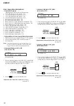
Page 32: ... SECTION 1 SERVICING NOTES 3 Application NVWriter for NV values rewriting How to get the application NVWriter for NV values rewriting Contact our service technical support section for PA products to get the application Pre check 1 Check the microcomputer version in this set For a checking method of the microcomputer version see SECTION 4 TEST MODE page 12 2 Check that the Net MD Driver has been in...

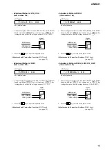
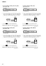
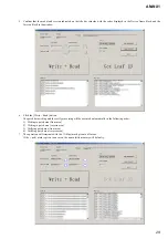
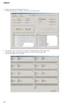
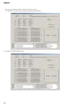
Page 33: ...o Servo 1 area front area 2 Writing to Servo 1 area reverse area 3 Writing to Power Supply 1 area front area 4 Writing to Power Supply 1 area reverse area 5 Writing to Power Supply 2 area front area 6 Writing to Power Supply 2 area reverse area 7 Verifying to Servo 1 area front area 8 Verifying to Servo 1 area reverse area 9 Verifying to Power Supply 1 area front area 10 Verifying to Power Supply ...

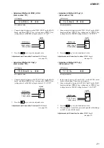
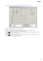
Page 34: ...34 AM NX1 7 The operation will terminate with Compere OK given to all areas If Compere NG is given to any area the nonvolatile memory will be faulty 8 Click the USB DISCONNECT button ...

Page 35: ...s 1 Select the manual mode of test mode see page 13 and set item number 071 2 Adjust with the VOL key adjusted value up or VOL key adjusted value down so that the adjusted value becomes 11 3 Press the key to write yhe adjustment value 4 Set item number 072 5 Adjust with the VOL key adjusted value up or VOL key adjusted value down so that the adjusted value becomes 01 6 Press the key to write yhe a...

Page 36: ...36 AM NX1 MEMO ...
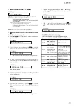
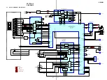
Page 37: ...F RST SE SSB CLK PD S0 PD S1 SSB DATA APCREF SYSTEM CONTROLLER DIGITAL SIGNAL PROCESSOR 16M BIT D RAM IC801 1 2 SIGNAL PATH PLAYBACK REC USB CHECK OUT USB CHECK IN A AOUTL 5 AOUTR 98 XMUTE 107 AOUT SEL 104 BEEP 175 UDP CLK SLCU SLCV SPCU SPCV SPCW SLD MON U SLD MON V CLV MON U CLV MON V CLV MON W SPRD SPDL MON SLDW SFDR SLDV SLDR SLD MON FRDR FFDR TRDR TFDR SPDV SPDW XRST MTR DRV RI1 FI1 RI2 FI2 W...

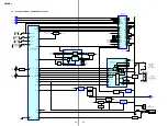
Page 38: ...STB 10 VC1 48 VREF 29 DTC2 19 DTC1 24 35 L2 36 VO2 D902 34 L2 42 VC2 40 REGI3 VCOUT REGC3 37 38 VCIN 47 44 REGI1 20 160 131 166 134 113 135 125 145 5 XWAKE1 VRMC 6 DATA SDO0 SCK0 SLEEP 58 CLK 63 XWAKE3 3 FFCLR 1 64 STRB 59 SCK 60 XWAKE4 2 VC1 B VG B REGC2 46 REGC1 45 REGO3 39 REG3 B REGO2 41 REG2 B REGO1 43 REG1 B VCO B REG2 B VREF 48 11 14 10 15 22 16 19 20 21 8 9 26 NOISE FILTER VREC B SWITCH SW...

Page 39: ...V and fed with regulated dc power supply from DC IN 3 V jack JK951 Voltages and waveforms are dc with respect to ground in playback mode no mark PLAYBACK REC USB Impossible to measure Voltages are taken with aVOM Input impedance 10 MΩ Voltage variations may be noted due to normal produc tion tolerances Waveforms are taken with a oscilloscope Voltage variations may be noted due to normal produc tio...

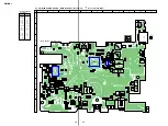
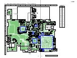
Page 40: ...12 C813 C830 R814 R817 R850 R815 R818 R813 L803 C807 C803 C808 R827 R826 C829 C828 C825 R841 C809 R829 C819 C838 R857 R834 R835 R825 R856 R823 R828 C810 R806 R872 R871 R805 C537 C529 C538 C534 C523 C533 C527 R508 R507 R510 C540 C511 C519 C514 C512 C520 IC501 C506 R511 C502 R958 R721 R723 R914 R713 R183 R605 C513 MAIN BOARD COMPONENT SIDE 11 11 1 687 890 TP951 CHGV TP961 CHGI_L TP962 CHGI_H TP952 G...

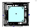
Page 41: ...LOCK ABX 1R OP FLEXIBLE BOARD 3 1 4 5 G1 S1 S1 D1 G2 S2 S2 D2 HR601 OVER WRITE HEAD BATTERY CASE 216 287 263 261 78 82 84 69 28 38 45 44 31 74 16 19 283 23 281 8 66 59 229 219 230 218 231 86 80 72 37 39 55 46 35 30 70 17 21 11 7 64 67 57 51 289 228 76 279 227 221 58 4 226 223 15 222 217 220 36 83 87 81 40 32 29 18 20 26 27 34 1 277 224 253 248 47 225 25 12 43 79 85 42 33 75 24 22 14 13 5 6 297 73 ...

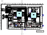
Page 42: ...N_U CLV_CON_V CLV_CON_W FCS FCS Z1 Z2 Z3 Z4 Z5 Z6 Z7 Z8 Z9 Z10 Z1 Z2 Z3 Z4 Z5 Z6 Z7 Z8 Z9 Z10 Z7 Z10 Y1 Y2 Y3 Y4 Y5 Y6 Y7 Y8 Y9 Y10 Y11 Y12 Y1 Y2 Y3 Y4 Y5 Y6 Y7 Y8 Y9 Y10 Y11 Y12 Y13 Y14 Y13 Y14 EXET_PWR PD_S1 PD_S0 PEAK BOTM TE RFI APCREF VC SLD_CON_W SLD_CON_V SLD_CON_U SLD_PWM SLD_MON_U SLD_MON_V SLD_MON_W XRST_MTR_DRV RECP S_MON ADIP TE NPPO TON C BOTM D A B C AVCC Jx Jy FE ABCD RFI ASSY CIG E...

Page 43: ...VDD DAVSS AVD1 AVS1 AVD2 AVS2 TSMVDD TSLVDD DRAMVDD0 DRAMVSS0 DRAMVDD1 DRAMVSS1 ITO MITY USBIFVDD MVDD USBOSCVDD USBOSCVSS AVDPLL AVSPLL EVA FVDD0 FVSS0 DVDD5 DVDD6 DRAMVDD3 DRAMVDD4 TEST1 TEST0 TRST SAK IDO NAR TAN TAT CS_RTC XRST SET_CODE3 SET_CODE2 SET_CODE1 SET_CODE0 UOSCO UPUEN SUSPEND UDM UDP RADIO_ON REC_KEY RMC_KEY HALF_LOCK_SW WK_DET HIDC_MON SET_KEY_2 SET_KEY_1 VREF_MON CHG_MON VB_MON JO...

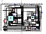
Page 44: ...p 0 01 0 1 0 1 1 0 47 6P FZT968TA SI2302DS T1 TS8K1TB 0 1 0 1 100k 470k 47 6 3V 47 6 3V 47 6 3V 47 6 3V 47 6 3V 47 6 3V CHGI_H CHGI_L 10 47 VREC XPC18A22AEPR2 CHG V GND 2P MCH6616 0 0 0 CPH5614 B1 B2 B3 B4 B5 B6 B7 B8 D1 D2 D3 D4 D5 D6 D7 D8 F1 F2 F3 F4 EFM HD_CON_1 HD_CON_2 MODE1 MODE2 MODE3 VREC_PWM VREF_MON WK_DET UDM UDP WK_DET CHG_ADSEL CHGI_SEL CHG_MON XRST_CHG EXET_PWR CHGI_CTL CHG_PWM HIDC...

Page 45: ... 22 6 3V 100 6 3V 100 6 3V 22 4V 4 7 6 3V 2 2 6 3V 2 2 6 3V 2 2 6 3V AK6510CL 0 1 0 01 0 01 4700p 2200p 4700p 2200p 1 1 1 0 01 0 01 1000p 1000p 1000p 0 01 1000p 0 1 1000p 0 01 1000p 0 1 0 01 1000p 1 1 2 2 220k 100k 470p 470p AN17020A VB SC901580EPR2 CL 270FG C TS UN9212J TX SO CL 270HR C TS VC1 4 7 16V REG2 VC2 REG3 REG1 0 1 0 01 0 1 100k MA2S111 TX 10k 220 2 5V 1M 1000p 1000p DF8A6 8FK TE85R C1 C...

Page 46: ...N DC IN DC IN DC IN VIO VIO VC VC VC VC VC2 VC2 VG VC VG VG2 SW VG2 VG3 VG3 VG2 VG VG VC VG2 OUTPUT SW 1 IX 2 PS 3 EQ 4 A GND 5 OFC C1 6 OFC C2 7 VREF10 8 VC 9 RFO 10 VREF09 11 AVCC2 AVCC2 AVCC AVCC2 12 PD NI 13 PD I 14 PD O D C A C AGND SMPN ADIP IN AGND AGND WPP LPF ADFG CON CCSL2 CLK CPGND NC 56 55 54 53 52 51 50 49 48 PEAK BOTM 47 46 45 42 FE 41 ABCD 40 RFI 39 ASSY 37 EFMO DGND RESET 34 VGIN 3...

Page 47: ...2 GND1 VC VG CPWO1 CPVO1 CPUO1 PWM1 UI1 VI1 WI1 PGNDW1 WO1 VMVW1 VO1 UO1 VMU1 VMR1 PGNDUV1 PGND1 FO1 VMF1 RO1 FI1 COM2 RI2 FI2 CPVI2 CPWI2 NC GND2 CPWI1 CPUI2 COM1 RI1 CPUI1 CPVI1 VI2 WI2 WO2 VO2 VMVW2 PGNDW2 UO2 VMU2 VMR2 PGNDUV2 PGND2 FO2 VMF2 RO2 3PHASE CONTROL CH1 3PHASE PRE DRIVER CH1 H BRIDGE PRE DRIVER CH1 H BRIDGE CONTROL CH1 V W U 3PHASE CONTROL CH2 3PHASE PRE DRIVER CH2 H BRIDGE PRE DRIV...

Page 48: ...I3 39 REGO3 38 CVIN 64 SLEEP 63 CLK 62 SEQSEL 61 WDT 60 SCK 59 STRB 58 DATA 57 HPI2 56 HPI1 55 MUTEON 54 GND 53 VHP1 52 HP1 51 PGND4 50 HP2 49 VHP2 PWM START UP SET UP DC DC CONVERTOR SET UP PRE DRIVER SERIES PASS REGULATOR1 CONTROL BANDGAP REFERENCE REF DAC SERIES PASS REGULATOR2 SERIES PASS REGULATOR3 POWER AWITCH 2 POWER AWITCH 1 LVB DRIVER REF1 REF2 REF3 REF3 REF4 REF5 XRST2 XRST2 FFCLR XRST1 ...

Page 49: ...ER OSC LOGIC SIGNAL RECEIVER VOLTAGE REFERENCE LOGIC SIGNAL RECEIVER VO VREF NSW1 VI2 VI VG N3 N2 N1 VI CAP_C_LIM VI2DET A D I_SEL AD_SEL VI2 RF1 PGND I_CTL1 I_CTL2 WK_DET PWR_WAKE VREF VREF SW4 SW5 SW6 NSW4 NSW3 BATT SEL VO VBAT IN2 OUT2 BAT_SEL VG VI IN1 WDT PWT CHG_CTL GND IC951 SC901582EPR2 ...

Page 50: ...ect terminal to the external capacitor for the low pass filter of CSL divider denominator 25 CCSL2 Connect terminal to the external capacitor for the TPP WPP low pass filter 26 CLK I System clock signal 256Fs 11 2896MHz input from the system controller 27 CPGND Ground terminal charge pump 28 CN Connected to the external capacitor for the charge pump 29 DVCC Power supply terminal 2 2V digital syste...

Page 51: ... from the optical pickup detector 51 B I Signal B input from the optical pickup detector 52 C I Signal C input from the optical pickup detector 53 AVCC Power supply terminal 2 3V analog system 54 JX I I V converted RF signal JX input from the optical pickup detector 55 JY I I V converted RF signal JY input from the optical pickup detector 56 IY I I V converted RF signal IY input from the optical p...

Page 52: ...plifier 20 ADIO O Monitor output terminal of A D converter input signal Not used 21 ADRB I The lower limit voltage of A D converter input terminal Not ised 22 SE I Sled error signal input from the RF amplifier 23 TE I Tracking error signal input from the RF amplifier 24 AUX1 I Auxiliary A D input terminal Not used 25 ADRT I The upper limit voltage of A D converter input terminal Not used 26 DCHG I...

Page 53: ...nitor signal output terminal Not used 69 TX O Record data output enable signal output Not used 70 RECP O Laser power changeover signal output Not used 71 EFMO O EFM encode data output for the record to the REC driver 72 TFMCK I FMCK signal input Not used 73 OFTRK I O Tracking signal input output Not used 74 XSKH O L circuit signal output Not used 75 XSKL O K SHOCK circuit signal output Not used 76...

Page 54: ...switch control signal output terminal Not used 119 120 NC O Not used 121 SLD_MON I Sled servo monitor signal input 122 VLON O Not used 123 SLEEP O System sleep control signal output to the power control H sleep 124 FFCLR O Input latch output for the start switching to the power control 125 CHGI_CTL1 O Charge current limit ON OFF control signal output at the time of adaptor use L limit ON 126 CHGI_...

Page 55: ...nce voltage monitor input A D input from the RF amplifier 162 SET_KEY_1 I Key input A D input from the switch liquid crystal display module 163 SET_KEY_2 I Key input A D input from the switch liquid crystal display module 164 CRADLE_DET I USB cradle or battery case detection signal input terminal 165 HIDC_MON I HIGH DC voltage monitor input terminal A D input 166 WK_DET I WAKE detection signal inp...

Page 56: ...ed at L 216 to 231 D0 to 15 DRAM data0 to 15 terminal Not used 232 to 245 A00 to 13 DRAM address0 to 13 terminal Not used 246 XCAS DRAM CAS terminal Not used 247 XRAS DRAM RAS terminal Not used 248 XWE DRAM write enable terminal Not used 249 XCS DRAM chip select terminal Not used 250 CLK DRAM clock terminal Not used 251 CKE DRAM clock enable terminal Not used 252 UDQM DRAM byte mask terminal Not u...

Page 57: ...nalog 283 AVS2 Ground terminal for the DSP servo system analog 284 TSMVDD Power supply terminal 2 4V for the TSB master communication 285 TSLVDD Power supply terminal 2 2V for the TSB slave I F 286 DRAMVDD1 Power supply terminal 2 2V for DRAM 287 DRAMVSS1 Ground terminal for DRAM 288 DRAMVDD2 Power supply terminal 2 2V for DRAM 289 DRAMVSS2 Ground terminal for DRAM 290 ITO Power supply terminal 2 ...

Page 58: ...et s Color Ref No Part No Description Remark Ref No Part No Description Remark 1 3 225 873 09 SCREW M1 4 for SILVER ORANGE 1 3 225 873 11 SCREW M1 4 for BLACK 2 X 3383 672 2 PANEL S SUB ASSY UPPER SILVER 2 X 3383 673 2 PANEL B SUB ASSY UPPER BLACK 2 X 3383 674 2 PANEL D SUB ASSY UPPER ORANGE 3 3 254 505 01 STRAPHOLE 4 X 3383 979 1 PANEL S SUB ASSY BOTTOM CE SILVER AEP UK 4 X 3383 980 1 PANEL B SUB...

Page 59: ... 528 01 SPRING R 60 3 234 449 11 SCREW M1 4 61 X 3382 650 1 TERMINAL PLUS ASSY BATTERY 62 3 246 497 02 TERMINAL BOARD AA BATTERY 63 A 3683 397 B MAIN BOARD COMPLETE for service E HK 63 A 4541 302 B MAIN BOARD COMPLETE for service AEP UK 64 3 238 876 04 SCREW M1 4 TOOTHED LOCK 65 3 246 519 01 BOARD MINUS TERMINAL 66 3 246 518 02 CASE BATTERY 70 3 254 713 01 SHEET DROP A 71 3 254 672 01 SHEET RADIAT...

Page 60: ... M1 4 EG PRECISION PAN 158 3 245 013 02 CHASSIS REC 159 3 245 021 02 PLATE RATCHET 0160 X 3382 955 1 OP SERVICE ASSY ABX 1R 161 A 3174 609 A SCREW BLOCK ASSY LEAD 162 X 3382 417 1 BASE ASSY MOTOR 163 X 3382 416 5 HOLDER ASSY 164 3 245 020 02 SPRING EJECT TENSION 165 3 244 879 01 SPRING RACK 166 4 997 677 21 WASHER 167 3 239 404 01 SCREW M1 4 M701 8 835 782 01 MOTOR DC SSM18D C NP SPINDLE M702 8 83...

Page 61: ...Items marked are not stocked since they are seldom required for routine service Some delay should be anticipated when order ing these items SEMICONDUCTORS In each case u µ for example uA µA uPA µPA uPB µPB uPC µPC uPD µPD CAPACITORS uF µF COILS uH µH The components identified by mark 0 or dotted line with mark 0 are critical for safety Replace only with part number specified When indicating parts ...

Page 62: ...43 1 164 943 11 CERAMIC CHIP 0 01uF 10 16V C844 1 125 777 11 CERAMIC CHIP 0 1uF 10 10V C845 1 107 819 11 CERAMIC CHIP 0 022uF 10 16V C851 1 125 777 11 CERAMIC CHIP 0 1uF 10 10V C901 1 100 396 11 TANTALUM CHIP 4 7uF 20 16V C902 1 137 858 11 TANTALUM CHIP 47uF 20 6 3V C903 1 137 858 11 TANTALUM CHIP 47uF 20 6 3V C904 1 137 858 11 TANTALUM CHIP 47uF 20 6 3V C905 1 137 858 11 TANTALUM CHIP 47uF 20 6 3...

Page 63: ...51 TRANSISTOR XP1210 TXE Q701 8 729 046 45 FET SI2302DS T1 Q702 8 729 427 74 TRANSISTOR XP4601 TXE Q703 8 729 427 74 TRANSISTOR XP4601 TXE Q704 8 729 046 45 FET SI2302DS T1 Q705 8 729 037 75 TRANSISTOR UN9214J TX SO Q721 8 729 039 86 TRANSISTOR FMMT717TA Q951 6 550 326 01 TRANSISTOR FZT968TA Q952 8 729 037 75 TRANSISTOR UN9214J TX SO Q1001 8 729 037 73 TRANSISTOR UN9212J TX SO RESISTOR R181 1 208 ...

Page 64: ...HIP 0 R844 1 218 990 11 SHORT CHIP 0 R845 1 218 957 11 RES CHIP 2 2K 5 1 16W R846 1 218 989 11 RES CHIP 1M 5 1 16W R847 1 218 965 11 RES CHIP 10K 5 1 16W R848 1 218 953 11 RES CHIP 1K 5 1 16W R849 1 218 957 11 RES CHIP 2 2K 5 1 16W R850 1 218 990 11 SHORT CHIP 0 R852 1 218 977 11 RES CHIP 100K 5 1 16W R853 1 218 977 11 RES CHIP 100K 5 1 16W R854 1 218 990 11 SHORT CHIP 0 R856 1 218 990 11 SHORT CH...

Page 65: ...14H 0504 1 477 507 12 CHARGE UNIT for BCA AM14H 505 3 252 271 01 FOOT RUBBER for BCA AM14H 506 1 542 529 12 HEADPHONE HP M170 507 1 477 744 12 REMOTE COMMANDER RC Z1C002 508 1 823 519 41 CORD CONNECTION DEDICATED USB CABLE 509 1 756 120 23 BATTERY NICKEL HYDROGEN NH 14WM 510 3 008 521 01 CASE BATTERY CHARGE 511 3 252 248 01 CASE CARRYING 512 1 251 895 11 BATTERY CASE 513 3 252 648 11 CLIP REMOTE C...

Page 66: ...ows you to jump to the revised page Also clicking the version at the upper right on the revised page allows you to jump to the next revised page Ver Date Description of Revision 1 0 2003 07 New 1 1 2003 08 Addition of E and Hong Kong Models ENG 03045 ...

Reviews: