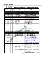
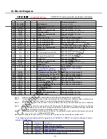
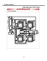
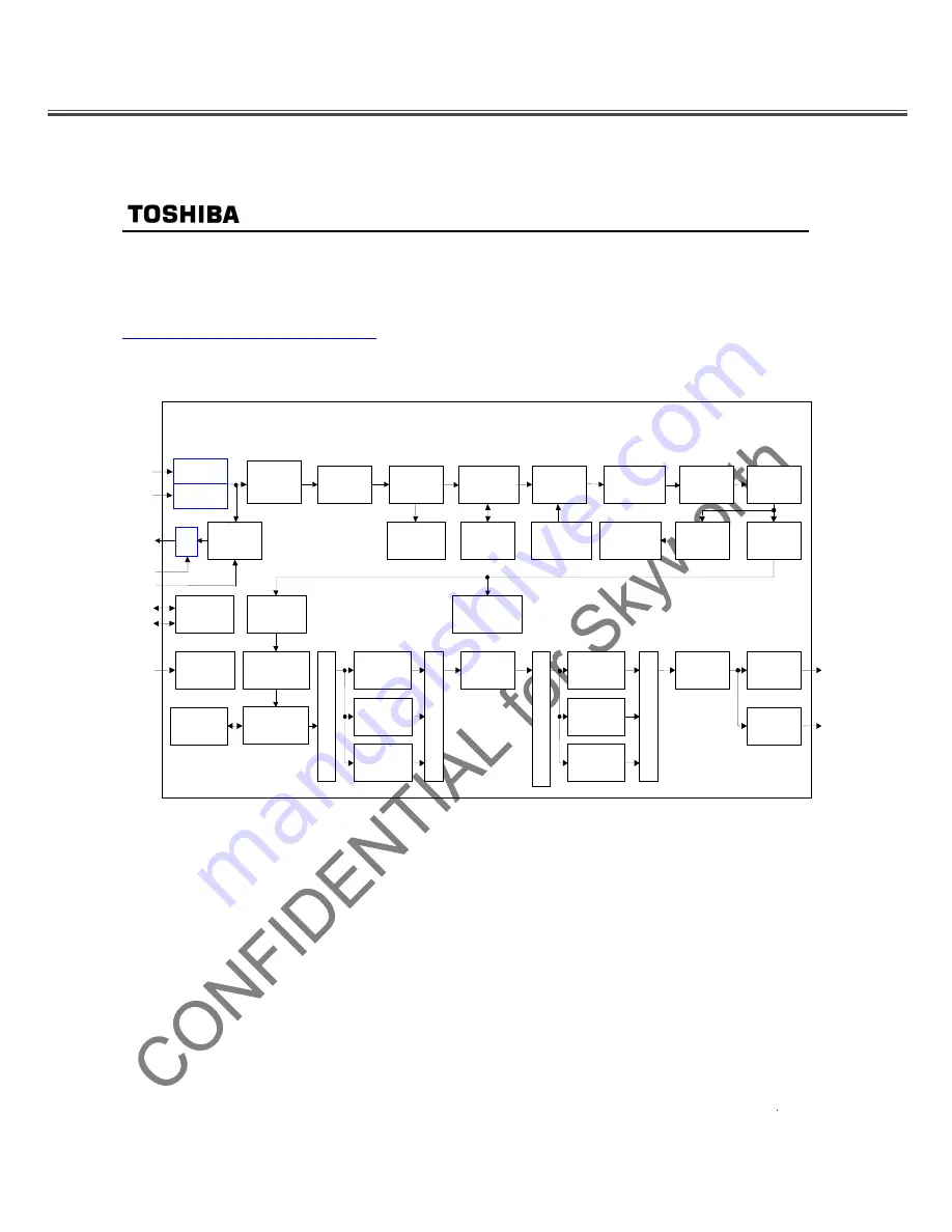
IC Block Diagram
-
25
-
TC9
0
517FG Toshiba products specification [Tentative]
CONFIDENTIAL
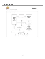
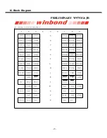
2.
Configuration
All functions required for ISDB-T demodulation and error correction are built into the TC9
0
517
.
The input signals to be supported are a low IF (intermediate frequency) signal and direct IF signal
.
Baseband IQ signals can also be input
.
The output signal is an MPEG-2 transport stream (TS) in serial format
.
Note that a TS in parallel format
can be output by setting registers
.
Fig
.
2
.
1 TC9
0
517FG Block Diagram
Synchroni-
zation flag
TS output
Crystal
(reference clock
)
Tuner
AGC
control
I
2
C
control
Filter
AGC
ISI
C
(unguarded
preecho/postecho
suppression)
FFT
Control
Adaptive
interpolation
filter
Equalization
CSI
(reliability
detection)
CVI
(CW interference
detection)
AGC control output
Tuner I
2
C
Clock PLL
Viterbi
decoding
Memory
Frequency
deinterleaving
RS
decoding
Error
detection
Output
control
Layer
isolation
TMCC
demodulation
Interpolation
phase
correction
Synchroni
zation
Demapping
CSI
processing
Bit
deinterleaving
B
y
te deinterleavin
g
TS
multiplex
FFT window
control
AGC distortion signal
ADC
ADC
IF input
or IQ input
SW
External AGC input
Host I
2
C
Energy
despreading
Energy
despreading
Energy
despreading
Demapping
CSI
processing
Demapping
CSI
processing
Modulation division
Quadrature
detection
AFC
Frequency
CPE
Pilot
extraction
Time
deinterleaving
Summary of Contents for 8M29B
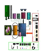
Page 3: ... 3 LCD 8M29B chassis ...
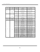
Page 5: ...For 42LED For 42LED 5 8 8 10 15 9800 12500 12500 266 276 9800 280 290 6500 313 329 ...
Page 6: ...40 40 3 2 1 4 2 50 0 5 80 40 12000 6 24 6 ...
Page 8: ... 8 4 ...
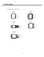
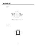
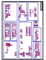
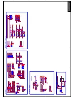
Page 19: ...IC Block Diagram 19 LM4558 MP1482DS BS IN SW GND SS EN COMP FB 1 2 3 4 8 7 6 5 TOP VIEW ...
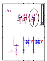
Page 20: ...IC Block Diagram 20 MST6M20S LF ...
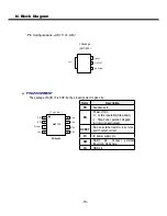
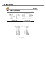
Page 23: ...IC Block Diagram 23 EN25F32 Figure 2 BLOCK DIAGRAM ...
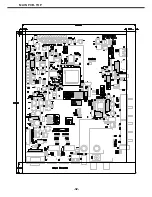
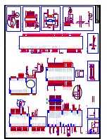
Page 32: ...MAIN PCB TOP 32 ...
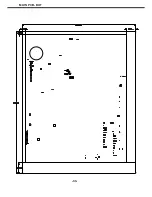
Page 33: ...MAIN PCB BOT 33 ...