Silicon Laboratories EFR32 1 Series Layout Design Manual Download Page 3

1.1  Matching Network Types for the 2.4 GHz EFR32 Series 1 Wireless MCU

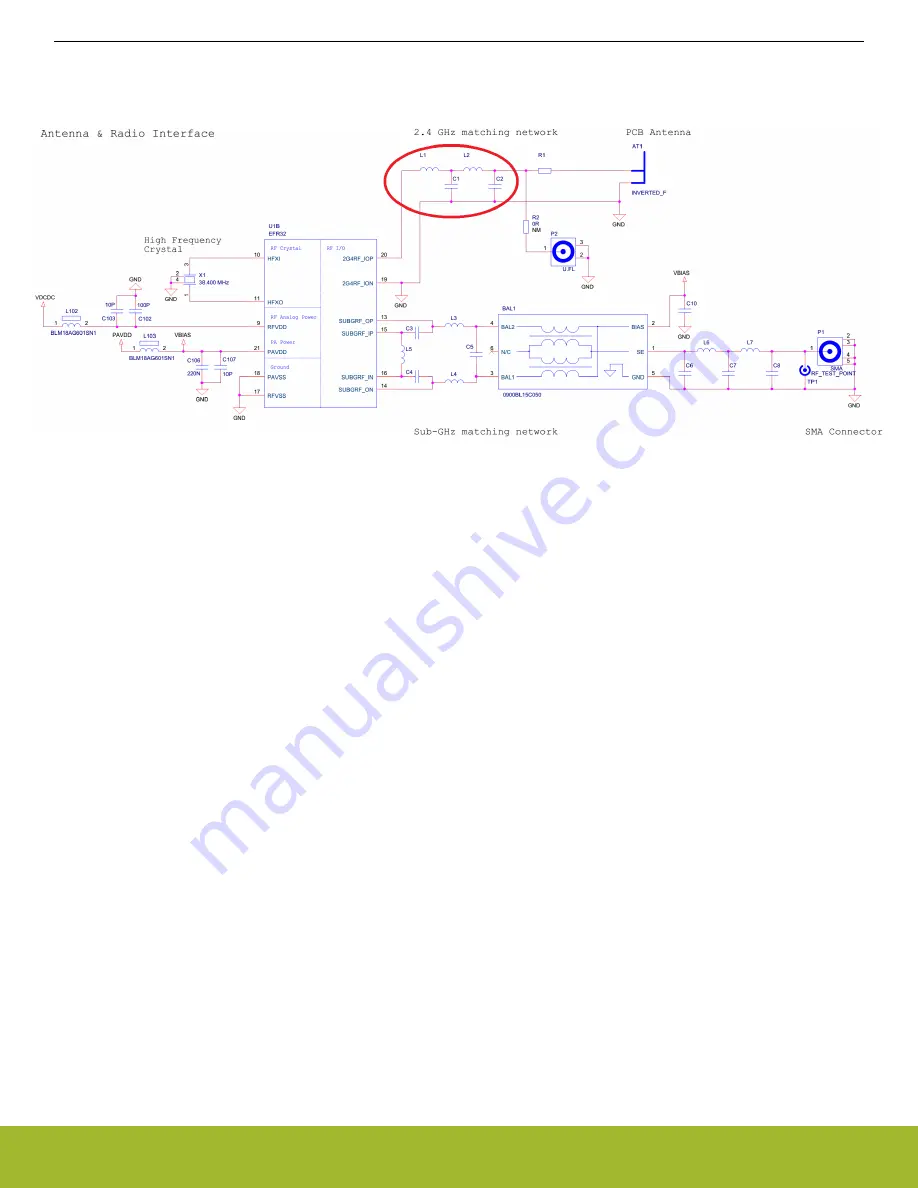
The antenna and radio interface schematic for the EFR32 Series 1 Dual-band (2.4 GHz and sub-GHz) Reference Radio Board is shown
in the figure below, the 2.4 GHz matching is highlighted by a red frame.

Figure 1.2.  Schematic of the RF Section for the EFR32 Series 1 Dual-band Reference Radio Board (2.4 GHz Matching is High-

lighted)

Note: 

Matching network component values for the 2.4 GHz frequency band should be chosen based on power range. For the correct

component values, refer to the reference designs. The 2.4 GHz-only EFR32 and the dual-band EFR32 have different pinouts. For the
correct pinout information, refer to the data sheet and reference designs.
 

The 2.4 GHz EFR32 Series 1 wireless MCU can provide m19.5 dBm power. All EFR32 Series 1 reference designs for 2.4
GHz use a series-L parallel-C ladder structured matching network. For low power applications (≤10 dBm) a 2-element L-C network is
sufficient, while high power solutions (>10 dBm) require a 4-element match.

It is not surprising that the increased TX output power of the EFR32 devices is accompanied by a corresponding increase in the abso-
lute level of harmonic signals. Since most regulatory standards (e.g. FCC, ETSI, ARIB etc.) require the harmonic signals to be attenu-
ated below some absolute power level (in watts or dBm), the amount of low-pass filtering required is generally greater on an RF radio-
board using an EFR32 that was designed for higher output power.

In the figure above, there is an additional component (R1) beside the 4-element matching, which is basically not part of the matching
network. The default value of R1 is 0 Ω. On 2.4 GHz-only radio boards that use the 2-element matching network, R1 is replaced by an
inductor to suppress the radiated 2nd harmonic. The proper value varies with antenna structure, in most cases 0 Ω can be used. For a
custom design, it is recommended to leave option for this series element, and its default value should be 0 Ω.

Further details on the 2.4 GHz matching network principles can be found in the application note, 

AN930.1: EFR32 Series 1 2.4GHz

Matching Guide

.

All EFR32 Series 1 radio boards for 2.4 GHz comprise a 50 Ω IFA (Inverted-F Antenna) connected to the 50 Ω output of the matching
network to be able to measure radiated performance. Optional conducted measurements are possible on these radio boards through an
U.FL connector.

AN928.1: EFR32 Series 1 Layout Design Guide

Design Recommendations When Using EFR32 Series 1 Wireless MCUs

silabs.com

 | Building a more connected world.

Rev. 0.5  |  3

Summary of Contents for EFR32 1 Series

Page 1: ...d debug environment In order to take advantage of the capabilities and features on custom hardware Silicon Labs recommends including debugging and programming interface connector s in custom hardware designs The details and ben efits of including these connector interfaces are detailed in AN958 Debugging and Pro gramming Interfaces for Custom Designs The power configurations and the proper usage o...

Page 2: ... and it is strongly recommended to use the same framed RF layout in order to avoid any possibility of detuning effects The figure below shows the framed compact RF part of the designs Figure 1 1 Top Layer of the Radio Board Left Side and Assembly Drawing of the RF Part Right Side The layout of the MCU VDD filtering capacitors should also be copied from the reference design as much as possible When...

Page 3: ... of harmonic signals Since most regulatory standards e g FCC ETSI ARIB etc require the harmonic signals to be attenu ated below some absolute power level in watts or dBm the amount of low pass filtering required is generally greater on an RF radio board using an EFR32 that was designed for higher output power In the figure above there is an additional component R1 beside the 4 element matching whi...

Page 4: ...he correct matching network information refer to the datasheet and reference designs The sub GHz EFR32 Series 1 wireless MCU can provide maximum 19 5 dBm power All sub GHz EFR32 matching network consist of the following sections impedance transformation circuit differential to single ended balun and low pass filter For further details on the sub GHz matching network principles refer to the applica...

Page 5: ... sitic caps to the ground However couplings between neighbor discretes may increase in this way To reduce the coupling between the nearby discrete inductors avoid placing them in the same orientation Use tapered line between transmission lines with different width i e different impedance to reduce internal reflections Avoid using loops and long wires to obviate their resonances They also work well...

Page 6: ...practices should be applied with a 2 element matching network as well Most of the layout guidelines in this section are general and should be applied in the sub GHz layout design as well The layout structure for the RF part of the EFR32 Series 1 Dual band Reference Radio Board is shown in the figure below the 2 4 GHz matching is highlighted by a blue frame Figure 2 1 Layout of the RF Section for t...

Page 7: ...ation between traces pads to the adjacent GND pour in the areas of the matching networks This techni que will minimize the parasitic capacitance and reduce the detuning effects If space allows the nearby inductors of the matching network should be kept perpendicular to each other to reduce coupling be tween stages This helps to improve filter attenuation at higher harmonic frequencies The series m...

Page 8: ...crystal and VDD traces to avoid any detuning effects on the crystal caused by the nearby power supply and to avoid the leakage of the crystal clk signal and its harmonics to the supply lines Figure 2 3 EFR32 Series 1 Layout Design Rules Dual band Reference Layout Top and Inner Layer 1 Use as many parallel grounding vias at the GND metal edges as possible especially at the edge of the PCB and along...

Page 9: ...nes on inner layers for boards with more than two layers Avoid placing the supply lines close to the PCB edge To reduce sensitivity to PCB thickness variations use 50 Ω grounded coplanar lines where possible for connecting the antenna or the U FL connector to the matching network This also reduces radiation and coupling effects A general rule is to use 50 Ω trans mission lines where the length of ...

Page 10: ...T 0 018 0 035 mm εr 4 6 H 0 325 mm G 0 25 mm W 0 45 mm Notes 1 Characteristic impedance is not super sensitive to the gap value It should be between 0 25 and 0 4 mm to have 47 through 53 Ω impedance 2 Different impedance calculators may yield slightly different results 3 H is the distance between the top and the first inner layer Figure 2 7 Grounded Coplanar Line Parameters AN928 1 EFR32 Series 1 ...

Page 11: ...t uses a 915 MHz matching similar design practices should be applied with matching networks for other sub GHz frequencies as well The layout structure for the RF part of the EFR32 Series 1 Dual band Reference Radio Board is shown in the figure below the sub GHz matching is highlighted by a blue frame Figure 2 8 Layout of the RF Section for the EFR32 Series 1 Dual band Reference Radio Board sub GHz...

Page 12: ...e chip As a result the first TX matching network components can be connected only with relatively long traces No traces should be routed on the layer beneath the traces that connects the first TX matching components with TX pins It is recommended to add an isolating ground metal with many vias between the 2 4 GHz and sub GHz matching networks The following figures illustrate layer consistency arou...

Page 13: ...tching Area on the EFR32 Series 1 Dual band Reference Layout Bottom layer AN928 1 EFR32 Series 1 Layout Design Guide Guidelines for Layout Design When Using EFR32 Wireless MCUs silabs com Building a more connected world Rev 0 5 13 ...

Page 14: ...und metal exist between the crystal and the RFVDD feed 7 Are the smallest value VDD filtering ca pacitors kept as close as possible to the VDD pins RFVDD PAVDD VREGVDD AVDD DVDD IOVDD of the EFR32 8 Are there multiple thermal straps used with the shunt capacitors 9 Do the ground pins of the shunt capaci tors use multiple vias 10 Does the exposed pad footprint use mul tiple vias 11 Is there at leas...

Page 15: ...ND metal edges closed by stitching vias where possible with a via distance less than lambda 10 of the highest usually 10th critical harmonic frequency 17 Are 50 Ω grounded coplanar lines used for RF traces longer than λ 16 at the fun damental frequency 18 Are there vias at the ground metalliza tion near the 50 Ω transmission lines 19 Are the RF related parts especially the antenna placed far away ...

Page 16: ...harmonic filtering capaci tors connected to ground planes on dif ferent sides of the transmission line 22 Is the area on the first inner layer be neath the RF chip and the matching net work filled with continuous GND metal and was wiring and routing avoided in this region AN928 1 EFR32 Series 1 Layout Design Guide Checklists silabs com Building a more connected world Rev 0 5 16 ...

Page 17: ...ied on all inner layers beneath the area of the RX matching network 26 Is the area on the first inner layer be neath the balun and low pass filter filled with continuous GND metal and was wiring and routing avoided in this re gion 27 Is wiring and routing avoided on the lay er beneath the traces that connect the first TX matching network components with TX pins AN928 1 EFR32 Series 1 Layout Design...

Page 18: ...ts The products are not designed or authorized to be used within any FDA Class III devices applications for which FDA premarket approval is required or Life Support Systems without the specific written consent of Silicon Labs A Life Support System is any product or system intended to support or sustain life and or health which if it fails can be reasonably expected to result in significant persona...

Reviews: