background image


SPC3 

PROFIBUS Interface Center 


SPC3 Hardware Description 

V1.3 

Page 29 

Copyright (C) Siemens AG 2003 All rights reserved. 


2003/04 

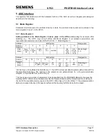
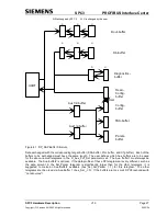
6.2  Description of the DP Services 

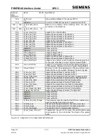
6.2.1  Set_Slave_Address (SAP55) 

6.2.1.1  Sequence for the Set_Slave_Address Utility 

The  user  can  disable  this  utility  by  setting  the  ‘R_SSA_Puf_Ptr  =  00H’  buffer  pointer.    The  slave  address 
must then be determined, for example, by reading a switch, and written in the R_TS_Adr. RAM register. 

The user must make a retentive memory possibility available (for example, EEPROM) to support this utility.  
It must be possible to store the ‘station address’ and the ‘Real_No_Add_Change’ (‘True’  = FFH) parameter 
in  this  external  EEPROM.    After  each  restart  caused  by  a  power  failure,  the  user  must  again  make  these 
values available to SPC3 in the R_TS_Adr und R_Real_No_Add_Change RAM register. 

If SAP55 is enabled and the Set_Slave_Address telegram is correctly accepted, SPC3 enters all net data in 
the  Aux-Puffer1/2,  exchanges  the  Aux  buffer1/2  for  the  SSA  buffer,  stores  the  entered  data  length  in 
‘R_Len_SSA_Data’, generates the ‘New_SSA_Data’ interrupt and internally stores the new ‘station address’ 
and  the  new  ‘Real_No_Add_Change’  parameter.    The  user  does  not  need  to  transfer  this  changed 
parameter  to  SPC3  again.    After  the  user  has  read  the  buffer,  the  user  generates  the 
‘SSA_Puffer_Free_Cmd’  (read  operation  on  address  14H).    This  makes  SPC3  again  ready  to  receive  an 
additional Set Slave Address telegram (such as from another master). 

SPC3 reacts independently when there are errors. 

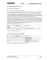
Address 

Bit Position 

Designation 

Control 
Register 


14H 

SSA_Puffer_Free_Cmd 


don´t care 


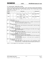
Figure 6.3:  Coding SSA_Buffer_Free_Cmd 
 

6.2.1.2  Structure of the Set_Slave_Address Telegram 

The net data are stored as follows in the SSA buffer: 

Byte 

Bit Position 

Designation 


New_Slave_Address 


Ident_Number_High 


Ident_Number_Low 


No_Add_Chg 

4-243 


Rem_Slave_Data additional application-
specific data 


Figure 6.4:  Data Format for the Set_Slave_Address Telegram 
 

Summary of Contents for SPC3

Page 1: ...SIMATIC NET SPC3 Siemens PROFIBUS Controller Hardware Description Date 2003 04 09 ...

Page 2: ......

Page 3: ...SIMATIC NET Siemens PROFIBUS Controller according to IEC 61158 Version 1 3 Date 2003 04 SPC3 Hardware Description ...

Page 4: ...te agreement The data in the document is tested periodically however Required corrections are included in subsequent versions We gratefully accept suggestions for improvement Copyright Copyright Siemens AG 2003 All Rights Reserved Unless permission has been expressly granted passing on this document or copying it or using and sharing its content are not allowed Offenders will be held liable All ri...

Page 5: ... Changes V 1 1 12 23 99 Chapter 8 2 Current consumption without bus accesses Chapter 10 1 Contact persons V 1 2 09 25 02 Included the specification of the different manufacturers in Chap 8 1 8 3 8 5 and 10 3 Order numbers chap 10 1 contact persons V 1 3 2003 04 Included the specification of the different manufacturers in Chap 8 1 8 3 8 5 and 10 3 ...

Page 6: ...r 25 5 4 1 Automatic Baud Rate Identification 25 5 4 2 Baud Rate Monitoring 25 5 4 3 Response Time Monitoring 25 6 PROFIBUS DP INTERFACE 26 6 1 DP_Buffer Structure 26 6 2 Description of the DP Services 29 6 2 1 Set_Slave_Address SAP55 29 6 2 2 Set_Param SAP61 30 6 2 3 Check_Config SAP62 31 6 2 4 Slave_Diagnosis SAP60 32 6 2 5 Write_Read_Data Data_Exchange Default_SAP 33 6 2 6 Global_Control SAP58 ...

Page 7: ...Motorola Mode E_Clock Mode for example 68HC11 50 8 5 5 Timing in the Asynchronous Motorola Mode for example 68HC16 52 8 5 6 Serial Bus Interface 54 8 5 7 Housing 55 8 5 8 Processing Instructions 56 9 PROFIBUS INTERFACE 57 9 1 Pin Assignment 57 9 2 Example for the RS 485 Interface 58 10 APPENDIX 59 10 1 Addresses 59 10 2 General Definition of Terms 60 10 3 Ordering of ASICs 60 10 3 1 SPC3 AMI 60 10...

Page 8: ...PROFIBUS Interface Center SPC3 Page 6 V1 3 SPC3 Hardware Description 2003 04 Copyright C Siemens AG 2003 All rights reserved ...

Page 9: ...gration of the complete PROFIBUS DP protocol the SPC3 decisively relieves the processor of an intelligent PROFIBUS slave The SPC3 can be operated on the bus with a baud rate of up to 12 MBaud However there are also simple devices in the automation engineering area such as switches and thermoelements that do not require a microprocessor to record their states There are two additional ASICs availabl...

Page 10: ... change buffers are provided for data communication both for the output data and for the input data A change buffer is always available for communication Therefore no resource problems can occur For optimal diagnostics support SPC3 has two diagnostics change buffers into which the user inputs the updated diagnostics data One diagnostics buffer is always assigned to SPC3 in this process The bus int...

Page 11: ...ata bus address bus multiplexed CPU memory 16 DB3 I O C165 mode data address bus separate 17 VSS 18 VDD 19 DB4 I O Data bus C32 mode data bus address bus multiplexed 20 DB5 I O C165 mode data bus address bus separate CPU memory 21 DB6 I O 22 DB7 I O 23 MODE I log 0 80C166 Data bus address bus separated ready signal log 1 80C32 data bus address bus multiplexed fixed timing System 24 ALE AS I Addres...

Page 12: ...PROFIBUS Interface Center SPC3 Page 10 V1 3 SPC3 Hardware Description 2003 04 Copyright C Siemens AG 2003 All rights reserved I CPD CMOS with pull down I TS TTLt Schmitt trigger ...

Page 13: ... global control command etc Corresponding to the parameter setting of the organizational parameters the user generated buffers are located beginning with address 40H All buffers or lists must begin at segment addresses 48 bytes segmentation Address Function 000H Processor parameters internal work cells Latches register 22 bytes 016H Organizational parameters 42 bytes 040H DP buffer Data In 3 Data ...

Page 14: ...he SPC 3 is divided logically into 192 segments Each segment consists of 8 bytes For more informations about the contents of the 3 memory areas see previous chapter The physical address is build by multiplikation with 8 Segment 0 Segment 1 Segment 191 Segment 190 8 Bit Segmentaddresses Pointer to the buffers Segment 2 0 10 internal SPC 3 RAM 1 5 kByte 0 7 ...

Page 15: ...ine 09H New_DIN_Buffer_Cmd 1 0 The user makes a new DP Din buffer available in the N state 0AH DOUT_Buffer_SM 7 0 Buffer assignment of the DP_Dout_Puffer_State_Machine 0BH Next_DOUT_Buffer_Cmd 1 0 The user fetches the last DP Dout Buffer from the N state 0CH DIAG_Buffer_SM 3 0 Buffer assignment for the DP_Diag_Puffer_State_Machine 0DH New_DIAG_Puffer_Cmd 1 0 The user makes a new DP Diag Buffer ava...

Page 16: ...Int Req_Reg 15 8 02H 03H Int Ack Reg 7 0 03H 02H Int Ack Reg 15 8 04H 05H Int Mask Reg 7 0 05H 04H Int Mask Reg 15 8 06H 07H Mode Reg0 7 0 Setting parameters for individual bits 07H 06H Mode Reg0 S 15 8 08H Mode Reg1 S 7 0 09H Mode Reg1 R 7 0 0AH WD Baud Ctrl Val 7 0 Root value for baud rate monitoring 0BH MinTsdr_Val 7 0 MinTsdr time OCH 0DH Reserved 0EH 0FH 10H 11H 12H 13H 14H 15H Figure 4 3 Ass...

Page 17: ...are Description V1 3 Page 15 Copyright C Siemens AG 2003 All rights reserved 2003 04 4 3 Organizational Parameters RAM The user stores the organizational parameters in RAM under the specified addresses These parameters can be written and read ...

Page 18: ...ntrol buffer belonging to it for example SSA Buf Prm Buf Cfg Buf Read Cfg Buf 2AH R Aux Puf Sel Bit array in which the assignments of the Aux buffers are defined to the control buffers SSA Buf Prm Buf Cfg Buf 2BH R_Aux_buf_Ptr1 Segment base address of auxiliary buffer 1 2CH R_Aux_buf_Ptr2 Segment base address of auxiliary buffer 2 2DH R_Len_SSA_Data Length of the input data in the Set_Slave_Addres...

Page 19: ...r 7 6 5 4 3 2 1 0 06H Intel Freeze_ Support ed Sync_ Support ed EARLY_ RDY INT_ POL MinTSDR DIS_ STOP_ CON TROL DIS_ START_ CON TROL Mode Reg0 7 0 Address Bit Position Designation Control Register 15 14 13 12 11 10 9 8 07H Intel Spec_Cle ar_Mode Spec_Prm_ Puf_Mode WD Test User Time base EOI Time base DP Mode Mode Reg0 13 8 When Spec_Clear_Mode Fail Safe Mode 1 the SPC3 will accept data telegramm w...

Page 20: ... data are accepted write 1 Ready is moved up by one clock pulse Bit 6 Sync_Supported Sync_Mode support 0 Sync_Mode is not supported 1 Sync_Mode is supported Bit 7 Freeze_Supported Freeze_Mode support 0 Freeze_Mode is not supported 1 Freeze_Mode is supported Bit 8 DP_MODE DP_Mode enable 0 DP_Mode is disabled 1 DP_Mode is enabled SPC3 sets up all DP_SAPs Bit 9 EOI_Time base Time base for the end of ...

Page 21: ...and goes to passive idle In addition the idle timer and Wd timer are started and Go_Offline 0 is set Bit 1 EOI End of Interrupt 1 End of Interrupt SPC3 switches the interrupt outputs to inactive and again sets EOI to log 0 Bit 2 Go_Offline Going into the offline state 1 After the current requests ends SPC3 goes to the offline state and again sets Go_Offline to log 0 Bit 3 User_Leave_Master Request...

Page 22: ...rrors the current SPC3 status and can be read only Address Bit Position Designation Control Register 7 6 5 4 3 2 1 0 04H Intel WD_State DP_State RAM access violation Diag_ Flag FDL_ IND_ST Offline Passive Idle Status Reg 7 0 1 0 1 0 Address Bit Position Designation Control Register 15 14 13 12 11 10 9 8 05H Intel SPC3 Release Baud Rate Status Reg 15 8 3 2 1 0 3 2 1 0 ...

Page 23: ...mory access 1 5kByte 0 No address violation 1 For addresses 1536 bytes 1024 is subtracted from the current address and there is access to this new address Bits 4 5 DP State1 0 DP State Machine state 00 Wait_Prm state 01 Wait_Cfg state 10 DATA_EX state 11 Not possible Bits 6 7 WD State1 0 Watchdog State Machine state 00 Baud_Search state 01 Baud_Control state 10 DP_Control state 11 Not possible Bit...

Page 24: ...he relevant bit position If a new event and an acknowledge from the previous event are present at the IRR at the same time the event remains stored If the processor subsequently enables a mask it must be ensured that no prior input is present in the IRR For safety purposes the position in the IRR must be deleted prior to the mask enable Prior to exiting the interrupt routine the processor must set...

Page 25: ...d a Global_Control telegram with a changed GC_Command Byte and this byte is stored in the R_GC_Command RAM cell Bit 9 New_SSA_Data The SPC3 has received a Set_Slave_Address telegram and made the data available in the SSA buffer Bit 10 New_Cfg_Data The SPC3 has received a Check_Cfg telegram and made the data available in the Cfg buffer Bit 11 New_Prm_Data The SPC3 has received a Set_Param telegram ...

Page 26: ...an be changed during operation All bits set Bit 1 Bit 0 Mask is set and the interrupt is disabled Mask is deleted and the interrupt is enabled 02H 03H Interrupt Acknowledge Register IAR Writable can be changed during operation All bits deleted Bit 1 Bit 0 The IRR bit is deleted The IRR bit remains unchanged Figure 5 5 Additional Interrupt Registers The New_Prm_Data New_Cfg_Data inputs may not be d...

Page 27: ...register 0 with SPC3 the watchdog is used for the DP_Control state after a Set_Param telegram was received with an enabled response time monitoring WD_On 1 The watchdog timer remains in the baud rate monitoring state when there is a switched off WD_On 0 master monitoring The PROFIBUS DP state machine is also not reset when the timer runs out That is the slave remains in the DATA_EXchange state for...

Page 28: ...R_SSA_Puf_Ptr must be set to 00H for this purpose The DDB utility is disabled by the already described initialization of the RAM cells The DP_SAP buffer structure is displayed in Figure 6 1 The user configures all buffers length and buffer beginning in the offline state During operation the buffer configuration must not be changed except for the length of the Dout Din buffers The user may still ad...

Page 29: ...r and Cfg buffer Each of the buffers to be exchanged must have the same length The user defines which Aux_buffers are to be used for the above named telegrams in the R_Aux_Puf_Sel parameter cell The Aux buffer1 must always be available The Aux buffer2 is optional If the data profiles of these DP telegrams are very different such as the data amount in the Set_Param telegram is significantly larger ...

Page 30: ... available in the Read_Cfg buffer for reading The Read_Cfg buffer must have the same length as the Cfg_buffer The Read_Input_Data telegram is operated from the Din buffer in the D state and the Read_Output_Data telegram is operated from the Dout buffer in the U state All buffer pointers are 8 bit segment addresses because the SPC3 internally has only 8 bit address registers For a RAM access SPC3 a...

Page 31: ...SPC3 enters all net data in the Aux Puffer1 2 exchanges the Aux buffer1 2 for the SSA buffer stores the entered data length in R_Len_SSA_Data generates the New_SSA_Data interrupt and internally stores the new station address and the new Real_No_Add_Change parameter The user does not need to transfer this changed parameter to SPC3 again After the user has read the buffer the user generates the SSA_...

Page 32: ...me base 10 ms WD_Base 1 time base 1 ms WD_Base 0 that is the time base is 10 ms 3 7 res to be parameterized with 0 0 Figure 6 5 Data Format for the Set_Param_Telegram 6 2 2 2 Parameter Data Processing Sequence In the case of a positive validatation for more than seven data bytes SPC3 carries out the following reaction among others SPC3 exchanges Aux Puffer1 2 all data bytes are input here for the ...

Page 33: ...s diagnostics bits are changed and there is branching to Wait_Prm For a correct configuration the transition to DATA_EX takes place immediately if no Din_buffer is present R_Len_Din_Puf 00H and trigger counters for the parameter setting telegrams and configuration telegrams are at 0 Otherwise the transition does not take place until the first New_DIN_Puffer_Cmd with which the user makes the first ...

Page 34: ...ag SPC3 responds during the next Write_Read_Data with high priority response data that signal the relevant master that new diagnostics data are present at the slave Then this master fetches the new diagnostics data with a Slave_Diagnosis telegram Then the Diag_Flag is reset again If the user signals Diag Stat_Diag 1 however static diagnosis see the structure of the diagnostics buffer then Diag_Fla...

Page 35: ...R_Len_Diag_Puf2 6 2 5 Write_Read_Data Data_Exchange Default_SAP 6 2 5 1 Writing Outputs SPC3 reads the received output data in the D buffer After error free receipt SPC3 shifts the newly filled buffer from D to N In addition the DX_Out_Interrupt is generated The user now fetches the current output data from N The buffer changes from N to U with the Next_Dout_Buffer_Cmd so that the current data of ...

Page 36: ...r_Cmd The user must delete the U buffer during initialization so that defined deleted data can be sent for a Read_Output Telegram before the first data cycle 6 2 5 2 Reading Inputs SPC3 sends the input data from the D buffer Prior to sending SPC3 fetches the Din buffer from N to D If no new buffer is present in N there is no change The user makes the new data available in U With the New_Din_buffer...

Page 37: ...r_Watchdog_Timer is implemented in SPC3 This User_Wd_Timer is an internal 16 bit RAM cell that is started from a R_User_Wd_Value15 0 value the user parameterizes and is decremented with each received Write_Read_Data telegram from SPC3 If the timer attains the 0000hex value SPC3 transitions to the Wait_Prm state and the DP_SM carries out a Leave_Master The user must cyclically set this timer to its...

Page 38: ... cell with 00H The user can read and evaluate this cell So that Sync and Freeze can be carried out these functions must be enabled in the mode register 6 2 7 Read_Inputs SAP56 SPC3 fetches the input data like it does for the Write_Read_Data Telegram Prior to sending N is shifted to D if new input data are available in N For Diag Freeze_Mode 1 there is no buffer change 6 2 8 Read_Outputs SAP57 SPC3...

Page 39: ...d by 2 Pin DIVIDER High Potential or 4 Pin DIVIDER Low Potential makes available on the pin CLKOUT2 4 as the system clock pulse so that a slower controller can be connected without additional expenditures in a low cost application SPC3 is supplied with a clock pulse rate of 48MHz 7 1 2 Bus Interface Unit BIU The BIU forms the interface to the connected processor microcontroller This is a synchrono...

Page 40: ...ignal 8 bit non multiplexed bus DB7 0 AB10 0 The following can be connected HC16 and HC916 types All other HC11 types with a multiplexed bus must externally select addresses AB7 0 from data DB7 0 The address decoder is switched off in SPC3 The CS signal is fed into SPC3 Chip select logic is available and programmable in all microcontrollers 0 1 Intel microcontroller CPU basis is 80C51 52 32 microc...

Page 41: ... 0 0000 00XXBIN W R RD INT0 Pulse Generator 48 MHz 80C32 20 16MHz Port 0 Port 2 CLK XW R XRD X INT AB8 AB9 AB10 80C32 System with Ext Memory C32 Mode 1K 1K 3K3 Mode GND VDD SPC3 Reset RTS TxD RxD XCTS 1K GND SPC3 Reset ALE Address Latch EPROM 64kB RAM 32kB Address Decoder AB 15 0 Reset PSEN SPC3 Reset SPC3 AB 7 0 Address decoder DB 7 0 Data DB 7 0 Address Latch A D 7 0 RD W R AB 7 0 Address decode...

Page 42: ...TR READY Logic Clock Generator 48 MHz 80286 Buscontr 82288 82244 DB AB CLK XWR XRD X INT XREADY 80286 System X86 Mode 3K3 Mode GND SPC3 Reset RTS TxD RxD XCTS 1K GND EPROM 64kB RAM 32kB Address Decoder Reset SPC3 12 24 MHz Teiler 2 4 DIVIDER AB 23 0 AB 12 1 DB 15 0 DB 7 0 XCS CS CSRAM CSEPROM Driver Control logic DB 7 0 AB 10 0 RD WR ...

Page 43: ...8 XINT MOT M 1K 33 XCTS 9 X INT 10 AB 10 14 13 7 XREADY XHOLDT CLK2 ADB 8 15 AB8 AB9 AB10 AB11 AB12 AB13 AB14 AB15 DB 0 7 ADB0 ADB1 ADB2 ADB3 ADB4 ADB5 ADB6 ADB7 TXD RTS RXD RS485 RS485 RS485 Px x uC uC uC uC uC SPC3 ALE XWR XRD INT0 1 1K M 5V or GND The pull up pull down resistances in the drawing above are only relevant for a in circuit tester The internal chip select logic is activated when the...

Page 44: ...485 RS485 RS485 uC uC uC uC SPC3 XWRL XRD XEXxIN 1 XCS uC XSPC3CS 23 MODE 1K M M 1K AB 0 10 uC AB8 AB9 uC XREADY AB10 10 10 5V or ground The pull up pull down resistances in the drawing above are only relevant for a in circuit tester Dual Port RAM Controller The internal 1 5k RAM of the SPC3 is a Single Port RAM Due to an integrated Dual Port RAM controller the controller however permits an almost...

Page 45: ...itter must hold back the first telegram character until the XCTS modem activates The receiver converts the serial data flow into the parallel data structure The receiver scans the serial data flow with the four fold transmission speed Stop bit testing can be switched off for test purposes DIS_STOP_CONTROL 1 in mode register 0 or Set_Param Telegram for DP One requirement of the PROFIBUS protocol is...

Page 46: ...h Voltage VIHC 0 7 VDD 0 7 V DD k A V DD V Input Low Voltage VILC k A 0 0 3 VDD 0 3 V DD V Schmitt Trigger CMOS Input High Voltage VP VIHC k A k A 0 8 VDD 4 V Input Low Voltage Vn VILC 0 2 VDD 1 k A k A V Hysteresis Voltage Vh 1 k A k A k A V Schmitt Trigger TTL Input High Voltage VP VIHC k A k A 2 1 2 4 V Input Low Voltage Vn VILC 0 7 0 6 k A k A V Hysteresis Voltage Vh 0 4 k A k A k A V Min Max ...

Page 47: ...rs AMI Vers ST Vers Input leakage current II 1 1 1 1 µA Tristate output leakage current IOZ 10 10 10 10 µA Tabelle 8 5 Leakage current of the output drivers 8 4 AC Specification for the Output Drivers Signal lineeitung Driver type Unit kap Last AMI Vers ST Vers DB 7 0 Tristate 8 8 mA 100pF TXD Tristate 8 8 mA 50pF RTS Tristate 8 8 mA 50pF X INT Tristate 8 4 mA 50pF XREADY XDSACK Tristate 8 4 mA 50...

Page 48: ...ulse No Parameter MIN MAX Unit Clock pulse 48 Mhz 1 Clock High Time 6 25 14 6 ns 2 Clock Low Time 6 25 14 6 ns 3 Rise Time 4 ns 4 Fall Time 4 ns Clock Pulse Timing 1 CLK 2 TCLH TCLL 2 4V 0 6V 3 4 Distortions in the clock pulse signal are permitted up to a ratio of 40 60 At a threshold of 1 5 or 3 5 V Interrupts No Parameter MIN MAX Unit 1 Interrupt Inactive Time for EOI_Timebase 0 1 1 µs Interrupt...

Page 49: ...PC3 is generated from the negative edge of the read signal and from the positive edge of the write signal AMI Vers ST Vers No Parameter Min Max Min Max Unit 1 Address to ALE Setuptime 10 10 ns 2 Address AB8 15 Holdtime after XRD or XWR 5 5 ns 3 XRD to Data Out Zugriff auf RAM 4T 5 88 3 3T 42 5 105 ns XRD to Data Out Zugriff auf die Register 4T 18 101 3 4T 20 2 103 5 ns 4 ALE to XRD 20 20 ns 5 Data...

Page 50: ...03 All rights reserved Synchronous Intel Mode Processor Read Timing XRD VALID ALE AB 7 0 DB 7 0 Data Out Adressen XWR log 1 13 Adressen VALID 12 8 1 2 4 3 5 10 14 Synchronous Intel Mode Processor Write Timing XWR VALID ALE AB 7 0 Data In Adressen XRD log 1 13 Adressen VALID DB 7 0 12 1 16 2 15 6 7 11 14 ...

Page 51: ... 21 XRD to Data valid Zugriff auf RAM 4T 5 88 3 3T 42 5 105 ns XRD to Data valid Zugriff auf die Register 4T 18 101 3 4T 20 2 103 5 ns 22 Address AB10 0 Holdtime after XRD or XWR 0 0 ns 23 XCS Setuptime to XRD or XWR 5 5 ns 24 XRD Puls Width 6T 10 115 6T 10 115 ns 25 Data Holdtime after XRD 2 6 3 1 10 2 ns 26 Read Write Inactive Time 10 10 ns 27 XCS Holdtime after XRD or XWR 0 0 ns 28 XRD XWR to X...

Page 52: ...ing XWR VALID AB 10 0 DB 7 0 XRD log 1 23 22 32 33 31 Data In XCS XREADY normal 27 30 28 20 26 29 34 XREADY early 36 37 8 5 4 Timing in the Synchronous Motorola Mode E_Clock Mode for example 68HC11 For a CPU clockline through the SPC3 the output clock pulse CLKOUT2 4 must be 4 times larger than the E_CLOCK That is a clock pulse signal must be present at the CLK input that is at least 10 times larg...

Page 53: ...5 5 ns 43 E_Clock to Data Active Delay 5 7 17 5 ns 44 E_Clock to Data valid Zugriff auf RAM 4T 5 88 3 3T 44 2 107 ns E_Clock to Data valid Zugriff auf die Register 4T 18 101 3 4T 21 9 105 2 ns 45 Data Holdtime after E_Clock 2 6 3 4 12 ns 46 R_W Setuptime to E_Clock 10 10 ns 47 R_W Holdtime after E_Clock 5 5 ns 48 XCS Setuptime to E_Clock 0 0 ns 49 XCS Holdtime after E_Clock 0 0 ns 50 Data Setuptim...

Page 54: ... No Parameter Min Max Min Max Unit 60 Address Setuptime to AS 0 0 ns 61 AS to Data valid Zugriff auf RAM 4T 5 88 3 3T 45 2 108 ns AS to Data valid Zugriff auf die Register 4T 18 101 3 4T 22 9 106 2 ns 62 Address AB10 0 Holdtime after AS 10 10 ns 63 R_W Setuptime to AS 10 10 ns 64 AS Puls Width Read 6T 10 6T 10 ns 65 Data Holdtime after AS 2 6 3 4 12 ns 66 AS Inactive Time 10 10 ns 67 R_W Holdtime ...

Page 55: ... to the register latches 3 For T 48MHz Asynchronous Motorola Mode Processor Read Timing AS VALID Data Out AB 10 0 DB 7 0 R_W E_Clock log 0 63 70 62 65 61 64 XDSACK normal XDSACK early 67 72 60 71 66 73 69 XCS 68 77 Asynchronous Motorola Mode Processor Write Timing AS VALID AB 10 0 DB 7 0 E_Clock log 0 63 62 75 76 74 Data In R_W XDSACK normal 67 72 70 60 66 69 XCS 68 71 73 XDSACK early 78 79 ...

Page 56: ... 3 SPC3 Hardware Description 2003 04 Copyright C Siemens AG 2003 All rights reserved 8 5 6 Serial Bus Interface No Parameter MIN MAX Unit Pulse 48 MHz 1 RTS to TxD Setup Time 4T 2 RTS to TxD Hold Token 4T T Clock pulse cycle 48MHz RTS TxD 1 2 ...

Page 57: ...SPC3 PROFIBUS Interface Center SPC3 Hardware Description V1 3 Page 55 Copyright C Siemens AG 2003 All rights reserved 2003 04 8 5 7 Housing PQFP 44 Housing ...

Page 58: ... β β 0 0 7 7 γ γ γ γ 0 1 5 9 G 0 13 0 20 H 1 95 J 0 30 0 30 K 0 40 2H Footprint 3 90 3 90 8 5 8 Processing Instructions ESD protective measures must be maintained for all electronic components SPC3 is a cracking endangered component that must be handled as such A drying process must be carried out before SPC3 is processed The component must be dried at 125o C for 24 hours and then be processed wit...

Page 59: ...B line Pin 4 Request to send RTS Pin 5 Ground 5V M5 Pin 6 Potential 5V floating P5 Pin 7 Free Pin 8 A line Pin 9 Free The cable shield must be connected to the plug connector housing The free pins are described as optional in EN 50170 Vol 2 If used they should conform to the specifications in DIN192453 CAUTION The designations A and B of the lines on the plug connector refer to the designations in...

Page 60: ...TS TXD RXD B line RTS 2M 2P5 A line Important electrical isolation to bus P5 and 2P5 Shield Driver select Differential voltage 2V 1 2 3 4 6 7 8 9 Layout lines must be kept as short as possible M 1M HCPL7101 7721 0721 2 2 22nF 500 V HCPL7101 7721 0721 5 Explanations of the circuitry The bus driver input EN2 has to be connected to low potential to ensure that after transmission of a telegram the ASI...

Page 61: ...1 9658 590 Technical contact person at ComDeC in Germany Siemens AG A D SE RD73 Mr Putschky Address Postfach 2355 90713 Fürth Tel 0911 750 2078 Fax 0911 750 2100 email Gerd Putschky siemens com Technical contact person at the PROFIBUS Interface Center in the United States PROFIBUS Interface Center One Internet Plaza PO Box 4991 Johnson City TN 37602 4991 Fax 423 262 2103 Your Partner Ron Mitchell ...

Page 62: ...pecification MS MicroSequenzer SM State Machine 10 3 Ordering of ASICs For Ordering SPC3 ASICs please refer to your contact person in the Siemens local branch office and use one of the ordering numbers depending on the amount you want to order 10 3 1 SPC3 AMI ASIC SPC 3 6ES7 195 0BD02 0XA0 Small amount 5 STEP C 6ES7 195 0BD12 0XA0 Single Tray 96 6ES7 195 0BD22 0XA0 Tray Box 576 6ES7 195 0BD32 0XA0...

Page 63: ...gnostics information are permanently specified in the firmware and in the micro program of the ASICs through the state machine Request diagnostics only once update_diag if an error is present or changes By no means should diagnostics be requested cyclically in the data exchange state otherwise the system will be burdened by redundant data Three information bits can be influenced by the application...

Page 64: ...r Byte 1 0 Identification Number Channel Number Coding Input Output Channel Number Type of Diagnostics Coding Channel Type Coding Error Type Coding of the error type is in part manufacturer specific other codings are specified in the Standard Example Status If the Bit EXT_DIAG is set to 0 data is viewed as status info from the system view f e cancellation of the error triggering the diagnostics 0 ...

Page 65: ...valuated After eliminating the current diagnostics situation this can be signalled as a status message from the slave without setting the external diagnostics bit With the COM ET200 a comfortable diagnostics tool is available on line At the present time identification related diagnostics information can be displayed with it in plain text In later phases channel related diagnostics will also be sup...

Page 66: ...iemens AG 2003 All rights reserved 12 Appendix B Useful Information 12 1 Data format in the Siemens PLC SIMATIC The SPC3 always sends data from the beginning of the buffer till the end 16Bit values are shown in the Motorola format For example Buffer pointer high byte Buffer pointer 1 low byte ...

Page 67: ......

Page 68: ...s AG Division Automation Engineering Combination Engineering Siemens AG PO Box 23 55 D 90713 Fuerth Germany Subject to change without prior notice SIEMENS Aktiengesellschaft Printed in the Fed Rep of Germany ...

Reviews: