2.4.2
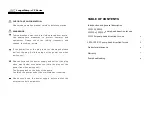
Digital IO Card
Circuits on the DIO board (DIO_I2C) are wired as shown in the following table. The table is
the view as seen when looking at the connector while the board is installed.
Table 2-1
DIO_I2C Wire Side View
Signal
Pin
Signal
DI Common 2
1 DI6
Digital Inputs: Optocoupler with internal 12-24VDC pow‐
er supply, switchable with floating contacts; alternative:
switchable with external voltage 12-24VDC, common
negative pole.
Digital Outputs: Digital Outputs: Floating double-throw
contacts, max. contact load rating 30V / 1A
The DOs are rated for 1A resistive load. Inductive loads
are different. A DO should not drive an inductive load
greater than 0.5A. The typical block and bleed applica‐
tion, which uses two parallel solenoids at 0.4A each,
should use separate DOs to drive each solenoid. Each
DO connected to a solenoid should have a diode to sup‐
press the solenoid load.
I/O Terminal Design: Plug-in terminal strips for stranded
or solid conductors with a maximum diameter of
1.0mm
2
or 18AWG.
DI Common 4
3 DI5
DI Common 6
5 DI4
DI Common 8
7 DI3
DI Common 10
9 DI2
DI Common 12 11 DI1
DO8 Common 14 13 DO8 NC
DO7 NC 16 15 DO8 NO
DO7 NO 18 17 DO7 Common
DO6 Common 20 19 DO6 NC
DO5 NC 22 21 DO6 NO
DO5 NO 24 23 DO5 Common
DO4 Common 26 23 DO4 NC
DO3 NC 28 27 DO4 NO
DO3 NO 30 29 DO3 Common
DO2 Common 32 31 DO2 NC
DO1 NC 34 33 DO2 NO
DO1 NO 36 35 DO1 Common
Figure 2-23 Digital IO Board (DIO_I2C)
Electronic Compartment Component Descriptions and Maintenance Procedures
2.4 Analog and Digital IO
Maxum II Reference Manual
58
Manual, 7/2017, 2000596-001