background image

Stage 3

Creating, testing and starting up the program:

Stage

Activity

1

Decide on the type of representation for the logic
blocks (LAD, CSF or STL, refer to Chapter 2).
Remember that function blocks can only be created in
the STL method of representation.

2

Program all logic and data blocks (please refer to your
STEP 5 manual).

3

Start up the blocks one after the other (you may have
to program a different OB for each individual step, to
call the logic blocks):
1a: load the block(s)
1b: test the block(s)

(For more detailed information please refer to your
STEP 5 manual and Chapter 11).

4

When you are certain that all the logic blocks run
correctly and all the data can be correctly calculated
and stored, you can start up your whole program.

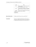
Note on test strategies

When you actually start up your program for the first time in genuine
process operation, i.e. with real input and more importantly output
signals, is a decision that must be left up to yourself or to a team of
experts.
The more complex the process, the greater the risk and therefore the
greater the care required when starting up.

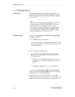
How to Tackle Programming

CPU 948 Programming Guide

C79000-G8576-C848-04

1 - 17

Summary of Contents for CPU 948

Page 1: ...ignment and Memory Organization 8 Memory Access Using Absolute Addresses 9 Multiprocessor Mode and Com munication in the S5 155U 10 PG Interfaces and Functions 11 Appendix 12 Indexes Abbreviations Key Words 13 The List of Operations order no 6ES5 997 3UA22 is included with this manual 10 98 C79000 G8576 C848 Release 04 S5 155U CPU 948 Programming Guide This manual has the order number 6ES5 998 3PR...

Page 2: ...led correctly and operated and maintained as recommended Trademarks SIMATICR SIMATIC NETR and SIMATIC HMIR are registered trademarks of SIEMENS AG Third parties using for their own purposes any other names in this document which refer to trademarks might infringe upon the rights of the trademark owners Wehavecheckedthecontentsofthismanualforagreementwiththe hardware and software described Since de...

Page 3: ...sentation 2 4 2 1 2 Structured Programming 2 5 2 1 3 STEP 5 Operations 2 6 2 1 4 Number Representation 2 8 2 1 5 STEP 5 Blocks and Storing them in Memory 2 12 2 2 Program Organization and Sequence Blocks 2 16 2 2 1 Organization Blocks as User Interfaces 2 18 2 2 2 Organization Blocks for Special Functions 2 22 2 3 Function Blocks 2 23 2 3 1 Structure of Function Blocks 2 24 2 3 2 Programming Funct...

Page 4: ...4 3 2 MANUAL and AUTOMATIC WARM RESTART 4 18 4 3 3 Comparison between COLD RESTART and WARM RESTART 4 21 4 3 4 RETENTIVE COLD RESTART 4 22 4 3 5 Comparison of COLD RESTART and RETENTIVE COLD RESTART 4 23 4 3 6 User Interfaces for Start Up 4 24 4 3 7 Extended AUTOMATIC WARM RESTART with the CPU 948 HOT RESTART 4 27 4 3 8 Interruptions during START UP 4 28 4 4 RUN Mode 4 29 4 4 1 Cyclic Program Exec...

Page 5: ...s 5 35 5 7 3 Settings 5 37 5 7 4 Error Handling 5 38 6 Integrated Special Functions 6 3 6 1 Introduction 6 4 6 2 OB 121 Set Read System Time 6 8 6 3 OB 122 Disable Interrupts On Off 6 12 6 4 OB 124 Delete STEP 5 Blocks 6 14 6 5 OB 125 Generate STEP 5 Blocks 6 17 6 6 OB 126 Define Transfer Process Images 6 20 6 7 OB 129 Battery State 6 25 6 8 OB 131 Delete ACCUs 1 2 3 and 4 6 26 6 9 OB 132 133 Roll...

Page 6: ...I RJ Area 8 14 8 3 4 RS RT Area 8 15 8 3 5 Bit Assignment of the System Data Words 8 18 8 3 6 Addressable System Data Area 8 42 9 Memory Access Using Absolute Addresses 9 3 9 1 Introduction 9 4 9 2 Memory Access via Address in ACCU 1 9 8 9 2 1 LIR TIR Loading to or Transferring from a 16 Bit Memory Area Indirectly 9 9 9 2 2 Examples of Access to DW 255 9 15 9 2 3 LDI TDI Loading to or Transferring...

Page 7: ...ters 10 24 10 3 Runtimes of the Communication OBs 10 31 10 4 INITIALIZE Function OB 200 10 33 10 4 1 Function 10 33 10 4 2 Call Parameters 10 35 10 4 3 Input Parameters 10 35 10 4 4 Output Parameters 10 38 10 5 SEND Function OB 202 10 40 10 5 1 Function 10 40 10 5 2 Call Parameters 10 40 10 5 3 Input Parameters 10 40 10 5 4 Output Parameters 10 42 10 6 SEND TEST Function OB 203 10 45 10 6 1 Functi...

Page 8: ...erial Link PG PLC via 1st or 2nd Serial Interface 11 16 11 4 Parallel Operation of Two Serial PG Interfaces 11 17 11 4 1 Installation 11 19 11 4 2 Operation 11 19 11 4 3 Sequence in Certain Operating Situations 11 21 11 5 PG Functions via the S5 Bus 11 27 11 5 1 Application 11 27 11 5 2 How the PG Functions Work via the S5 Bus 11 29 11 5 3 Installation and Getting Started 11 31 11 5 4 Condition Co...

Page 9: ...e Programs in a CPU 1 7 1 4 Which Operands are available to the User Program 1 11 1 5 How much Memory is available for the User Program 1 14 1 6 How to Tackle Programming 1 15 1 7 Programming Tools 1 18 1 8 Converting User Programs of the CPU 928B for the CPU 948 1 19 1 Introduction CPU 948 Programming Guide C79000 G8576 C848 04 1 1 ...

Page 10: ...Contents CPU 948 Programming Guide 1 2 C79000 G8576 C848 04 ...

Page 11: ...Chapter 1 explains how to use the manual and deals with the areas of application of the S5 155U programmable controller with the CPU 948 and its structure The chapter explains the typical mode of operation of a CPU and the structure of the CPU program You will also find a few suggestions about how to tackle programming and will learn some of the features of the CPU 948 which are important for prog...

Page 12: ... and word oriented processing and fast reaction times i e with extremely fast open and closed loop controls Examples of this are fast processes in mechanical engineering bottling plant packing machines or similar systems and in the automobile industry Tasks requiring an extremely high storage capacity and fast access times e g in the automobile industry process and plant engineering Tasks requirin...

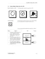
Page 13: ... inputs PII 2 The values contained in the PII are processed by the user program and the values to be output are entered in the process image of the outputs PIQ 3 The values contained in the process image of the outputs are output by the system program to the output modules assigned to the CPU Cyclic processing Interrupt driven processing Time controlled processing 1 2 3 Read in process image of th...

Page 14: ...special processing section within your program Processing according to priority The types of processing listed above are handled by the CPU according to their priority Since a fast reaction is required to a time or interrupt event the CPU interrupts cyclic processing to handle a time or interrupt event Cyclic processing therefore has the lowest priority Whether or not the time controlled processin...

Page 15: ...ons and sequences of the CPU which do not involve a specific control task refer to Fig 1 2 Update process image of the inputs Output process image of the outputs System program Call user processing inter faces Execute start up Handle errors Communication with the PG Manage memory Fig 1 1 Tasks of the system program The Programs in a CPU CPU 948 Programming Guide C79000 G8576 C848 04 1 7 ...

Page 16: ... power supply to the PLC POWER UP the system program is read from the EPROM to the internal operating system RAM System program defaults The following chapters except for Chapter 7 describe the default system reaction to process events or errors Depending on the defaults the CPU changes to the stop mode if an operation code error occurs and the error organization block is not loaded Modifying the ...

Page 17: ...igning specific values to signals Cyclic processing Constantly repeated signal processing e g logic operations on binary signals reading in and analyzing analog values specifying binary signals for output outputting analog values Time controlled processing Special time dependent processing with the following time conditions faster than the average cycle at a time interval greater than the average ...

Page 18: ... 8 SEGMENT 1 NAME TRANS 0005 L IB 3 0006 T FW 200 0007 C DB 5 0008 DO FW 200 0009 L DW 0 000A T QW 6 000B BE 1 KH 0101 2 KF 120 3 KS xy 4 KY 4 5 5 KG 6 KM 7 1 KH FFFF 2 KH FFFF 3 KH FFFF 4 KH FFFF 5 KH FFFF 6 KH FFFF 7 STEP 5 operations static or dynamic data bits bytes words double words static or dynamic data bits bytes words double words STEP 5 operations STEP 5 operations STEP 5 operations Pro...

Page 19: ... bits bytes words double words 128 bytes each for inputs and outputs I O area P area Characteristics Size The user program can access the I O modules directly via the S5 bus The following data types are possible bytes words 256 bytes each for inputs and outputs Extended I O area O area Characteristics Size The user program can access the I O modules directly via the S5 bus The following data types...

Page 20: ... the cycle via a buffer in the coordinator or CP IP 2048 bits S flags extended flag area Characteristics Size The CPU 948 also contains an additional flag area the S flag area The user program can also access this area extremely quickly as with the F flags S flags cannot however by used as actual operands with function block calls nor as IPC flags for data exchange between the CPUs The bit test op...

Page 21: ...ters Data words in the current data block Characteristics Size A data block contains constants and or variables in the byte word or double word format With STEP 5 operations you can always access the current data block refer to Section 2 4 2 The following data types can be accessed single bits bytes words double words 256 words 1 1 In data blocks with a length greater than 256 words you can only a...

Page 22: ... blocks the CPU 948 only has the user memory in the internal RAM The CPU 948 is available with two versions of the user memory Version 1 with 640 Kbytes Version 2 with 1 664 Kbytes How much Memory is available for the User Program CPU 948 Programming Guide 1 14 C79000 G8576 C848 04 ...

Page 23: ...ram 3 Creating testing and starting the program Recursive procedure In practice you will recognize that certain steps must be repeated recursive procedure e g when you realize that more signals are required to improve the handling of the task Stage 1 Determining the technological task Stage Activity 1 Create a general block diagram outlining the control tasks of your process 2 Create a list of the...

Page 24: ...ta for flags and data blocks which may be required Create flow diagrams for the logic blocks Notes on the scope of cyclic processing When deciding on the types of processing keep the following conditions in mind The cycle must run through quickly enough The process statuses must not change more quickly than the CPU can react Otherwise the process can get out of control The maximum reaction time sh...

Page 25: ...st the block s For more detailed information please refer to your STEP 5 manual and Chapter 11 4 When you are certain that all the logic blocks run correctly and all the data can be correctly calculated and stored you can start up your whole program Note on test strategies When you actually start up your program for the first time in genuine process operation i e with real input and more important...

Page 26: ...P 5 programming language Here you require the STEP 5 programming package along with the system software STEP 5 ST or STEP 5 MT description refer to 3 in Further Reading or In a higher programming language If you are familiar with programming in higher programming languages you can also formulate your STEP 5 program for the CPU 948 as follows SCL refer to 12 in Further Reading the SCL compiler is c...

Page 27: ...ecessary Block transfer opera tion TNB 16 bit long addresses are used The operation does not exist Use TNW for block transfer from the 8 bit to the 8 bit area Block transfer opera tion TNW 16 bit long addresses are used Block transfers from the 8 bit to the 8 bit area and vice versa are possible 20 bit long addresses are used Adaptation is necessary only block transfers from the 8 bit to the 8 bit...

Page 28: ... CPU 928B CPU 948 Process interrupts have higher priority than timed interrupts Timed interrupts have priority over process interrupts via IB 0 or system interrupts You can change the priority with the parameters in DX 0 Data block DB 0 block address list CPU 928B CPU 948 The block address list contains the direct start addresses of the blocks The block address list contains the segment addresses ...

Page 29: ...e on the CPU 928B and CPU 948 Error OBs The following error OBs of the CPU 948 respond differently from their namesakes on the CPU 928B OB Function Error IDs OB 19 OB 26 OB 27 Same as on CPU 928 Different from CPU 928B OB 28 OB 29 OB 30 OB 31 Function different from that on CPU 928B Special function OBs OB Note OB 110 OB 152 OB 160 to 163 OB 170 OB 190 to 193 OB 216 to 218 OB 220 and 221 OB 224 OB...

Page 30: ...ion In contrast to the CPU 928B these CPU 948 OBs change the content of ACCU 4 R64 controller software The R64 controller software cannot be run on the CPU 948 Standard FBs Generally the standard function blocks used on the CPU 928B e g for IPs must be replaced by those for the CPU 948 The HDBs are an exception these can be taken from the CPU 928B see Section 1 8 1 Converting User Programs of the ...

Page 31: ...ks 2 16 2 2 1 Organization Blocks as User Interfaces 2 18 2 2 2 Organization Blocks for Special Functions 2 22 2 3 Function Blocks 2 23 2 3 1 Structure of Function Blocks 2 24 2 3 2 Programming Function Blocks 2 26 2 3 3 Calling Function Blocks and Assigning Parameters to them 2 28 2 3 4 Special Function Blocks 2 33 2 4 Data Blocks 2 35 2 4 1 Creating Data Blocks 2 37 2 4 2 Opening Data Blocks 2 3...

Page 32: ...Contents CPU 948 Programming Guide 2 2 C79000 G8576 C848 04 ...

Page 33: ...2 User Program The following chapter explains the components that make up a STEP 5 user program for the CPU 948 and how it can be structured CPU 948 Programming Guide C79000 G8576 C848 04 2 3 ...

Page 34: ...ould use system operations 2 1 1 The LAD CSF STL Methods of Representation When programming in STEP 5 you can choose between the three methods of representation ladder diagram LAD control system flowchart CSF and statement list STL for each individual logic block You can choose the method of representation that best suits your particular application The machine code MC5 that the programmers PGs ge...

Page 35: ...his division of your program clarifies the essential program structures making it easy to recognize the system parts that are related within the software Ladder diagram Statement list Control system flowchart Programming with graphic symbols like a circuit diagram Programming with graphic symbols IEC 117 15 DIN 40700 DIN 40719 DIN 19239 DIN 19239 DIN 19239 STL CSF LAD A AN A ON O 1 I I I I I Q Pro...

Page 36: ...ntiate between blocks that contain statements code i e organization blocks program blocks function blocks or sequence blocks and blocks that contain data data blocks 2 1 3 STEP 5 Operations A STEP 5 operation is the smallest independent unit of the user program It is the work specification for the CPU A STEP 5 operation consists of an operation and an operand as shown in the following example Exam...

Page 37: ...r values compare values and process them arithmetically specify timer and counter values convert number representations call blocks and execute jumps within a block and influence program execution Result of logic operation RLO The central bit for controlling the program is the result of logic operation RLO This is obtained as a result of binary logic operations and is influenced by some operations...

Page 38: ...e programmer converts the internal representation into the form you have requested Permitted operations You can carry out all arithmetic operations with the 16 bit fixed point numbers and floating point numbers including comparison addition subtraction multiplication and division Note Do not use BCD coded numbers for arithmetical operations since this leads to incorrect results Use 32 bit fixed po...

Page 39: ...ixed point numbers for simple calculations and for comparing number values Since fixed point numbers are always whole numbers remember that the result of dividing two fixed point numbers is also a fixed point number without decimal places Floating point numbers Floating point numbers are positive and negative fractions They always occupy a double word 32 bits A floating point number is represented...

Page 40: ... the sign is 1 it is a negative number in its two s complement representation The floating point value 0 is represented as the binary value 80000000H 32 bits see below Coding floating point numbers Coding a floating point number 31 30 24 23 22 0 V 26 20 V 2 1 2 23 Exponent Mantissa Specification of the data format for floating point numbers at the PG KG Permissible numerical range 0 1469368 x 10 3...

Page 41: ...inary numbers between 0000 and 1001 0 and 9 decimal The left bits are reserved for the sign as follows Sign for a positive number 0000 Sign for a negative number 1111 Permissible numerical range 999 to 999 PG display after you enter the line L KG 1234567 02 Mantissa with sign Exponent base 10 with sign Value of the number input 0 1234567 x 10 2 12 34567 PG display after you enter the line 6 KG 500...

Page 42: ...gram OBs 40 to 100 are blocks belonging to the operating system You must not call these blocks OBs 121 to 255 contain special functions of the system program You can call these blocks if required in your user program Program blocks PB You require program blocks to structure your program They contain program parts divided according to technological and functional criteria Program blocks represent t...

Page 43: ...am works This type of block contains no STEP 5 statements and has a distinctly different function from the other blocks Using block type DX doubles the number of possible data blocks Formal structure of the blocks All blocks consist of the following two parts a block header and a block body Block header The block header is always 5 words long and contains information for block management in the PG...

Page 44: ...imum length A STEP 5 block can occupy a maximum of 32 767 words in the program memory of the CPU 1 word corresponds to 16 bits Available blocks You can program the following block types Data blocks DB 0 DB 1 DB 2 DX 0 DX 1 and DX 2 contain parameters These are reserved for specific functions and you cannot use them as normal data blocks Data block DX 2 is reserved for the 2nd serial interface and ...

Page 45: ...mory and a new block is entered Similarly when blocks are deleted they are not really deleted instead they are declared invalid The space they occupy is however not released and is not available for blocks loaded later Note You can use the COMPRESS MEMORY online function to make space for new blocks This function optimizes the utilization of the memory by deleting blocks marked as invalid and shif...

Page 46: ...your program in the STEP 5 programming language When programming PBs OBs and SBs you can only use the STEP 5 basic operations A STEP 5 block should always be a self contained program section Logic operations must always be completed within a block 3 Complete your program input with the block end operation BE Block calls With the exception of OB 1 to OB 39 you must call the blocks to process them U...

Page 47: ...le JU PB 100 Conditional call The JC statement belongs to the conditional operations The addressed block is processed only if the previous RLO 1 If the RLO 0 the jump is not executed Example JC PB 100 Note After the conditional jump operation is executed the RLO is set to 1 regardless of whether or not the jump to the block is executed PB 1 PB 5 PB 10 PB 6 BE BE BE BE A A O I 1 0 I 2 0 I 3 0 JU PB...

Page 48: ...locks form the interfaces between the system program and the user program Organization blocks OB 1 to OB 39 belong to your user program just as program blocks By programming these OBs you can influence the behavior of the CPU during start up program execution and in the event of an error The organization blocks are effective as soon as they are loaded in the PLC memory This is also possible while ...

Page 49: ...errupt lines of the S5 bus System interrupt INT X INT A B C or D depends on slot System interrupt INT E System interrupt INT F System interrupt INT G Delayed interrupt Clock controlled interrupt OB 10 OB 11 OB 12 OB 13 OB 14 OB 15 OB 16 OB 17 OB 18 Organization of time controlled program execution timed interrupt with selectable basic clock rate default T 100 ms and clock distributor default corre...

Page 50: ...eaction to device or program errors 1 Block Function and call criterion OB 19 Runtime error LZF called block not loaded PB SB FB FX or attempt to open a data block that is not loaded DB DX OB 23 Timeout QVZ in user program during direct access to I O modules OB 24 Timeout QVZ when updating the process image and transferring interprocessor communication flags OB 25 Addressing error ADF OB 26 Cycle ...

Page 51: ...an error EXCEPTION if OB 19 logic block not loaded OB 23 or OB 24 OB 29 timeout or OB 33 collision of timed interrupts do not exist there is no reaction 2 OB 31 only exists in the CPU 948 for the sake of compatibility To set the cycle monitoring time you should use data block DX0 refer to Chapter 7 OB 31 is called once during the start up if loaded You can also use it to set the cycle monitoring t...

Page 52: ...Roll down ACCU OB 141 Enable disable disable individual timed interrupts OB 142 Enable disable delay all interrupts OB 143 Enable disable delay single timed interrupts OB 150 Set read system time compatible with CPU 928B OB 151 Set read clock controlled interrupt time OB 153 Set read time for delayed interrupt OB 180 Variable data block access OB181 Test data blocks DB DX OB 182 Copy data area OB ...

Page 53: ...r fast and simple open loop control signalling closed loop control and logging or you can program function blocks yourself Compared with organization program and sequence blocks function blocks have the following four essential differences OB PB SB FB FX 1 Range of operations only basic operations basic operations supplementary operations system operations 2 Method of representation programming an...

Page 54: ...y This jump statement is not displayed when the function block is displayed on the PG When a function block is called only the block body is processed Absolute or symbolic operands You can enter operands in a function block in absolute form e g F 2 5 or symbolically e g MOTOR1 You must store the assignment of the symbolic operands in an assignment list before you enter the operands in a function b...

Page 55: ...transfer to the calling program You define the input operands and output results as formal operands These function as tokens When a block is called by a higher order block OB PB SB FB FX the formal operands block parameters are replaced by actual operands i e parameters are assigned to the function block How to program IF THEN You want to program a function block directly i e without formal operan...

Page 56: ...aracters and must start with a letter 3 If the function block is to process formal operands Enter the formal operands you require in the block as block parameters Enter the following information for each formal operand the name of the block parameter maximum 4 characters the type of block parameter and the data type of the block parameter if applicable You can define a maximum of 40 formal operand...

Page 57: ...meters Parameter type Data type I input parameter Q output parameter BI BY W D D data KM KH KY KS KF KT KC KG B block operation T timer C counter none no type can be specified I D B T or C are parameters that are indicated to the left of the function symbol in graphic representation Parameters labelled with Q are indicated on the right of the function symbol The data type indicates whether you are...

Page 58: ...f the formal operands i e you assign parameters to the function block These actual operands can be different for separate calls e g inputs and outputs for the first call of FB 200 flags for the second call Using the formal operand list you assign the required actual operands for each function block call none Unconditional conditional call Unconditional call Conditional call JU FBn for FB function ...

Page 59: ...te from extended periphery IW n input word QW n output word FW n flag word DW n data word PW n peripheral word OW n word from extended periphery ID n input double word QD n output double word FD n flag double word DD n data double word D KM for a binary pattern 16 bits KY for two absolute numbers one byte each each in the range from 0 to 255 KH for a hexadecimal pattern with a maximum of four digi...

Page 60: ...possible T 0 to 255 Timer C Data type designation not possible Z 0 to 255 Counter 1 0 1469368 x 10 38 to 0 1701412 x 1039 Note S flags are not permitted as actual operands for function blocks After the jump to a function block the actual operands from the block then called are used in the function block program instead of the formal operands This feature of programmable function blocks allow them ...

Page 61: ...D B T C Q BI BY W D BI A INP1 A INP2 OUT1 BE Function block FB 202 is called and has parameters assigned to it in program block PB 25 STL method of representation CSF LAD method of representation PB 25 SEGMENT 1 JU FB 202 FB 202 NAME EXAMPLE EXAMPLE INP1 I 13 5 I 13 5 INP1 OUT1 Q 23 0 INP2 F 17 7 F 17 7 INP2 BE OUT1 Q 23 0 BE The following operations are executed after the jump to FB 202 Formal op...

Page 62: ...GMENT 1 C DB 5 JU FB 201 NAME REQUEST DATA DW 1 RST I 3 5 SET F 2 5 MTIM T 2 TIME KT 010 1 TRAN DW 2 BEC Q 2 3 LOOP Q 6 0 BE CSF LAD method of representation PB 25 SEGMENT 1 FB 201 REQUEST DW 1 DATA TRAN DW 2 I 3 5 RST BEC Q 2 3 F 2 5 SET LOOP Q 6 0 T 2 MTIM BE KT 010 1 TIME Formal operands Actual operands Function Blocks CPU 948 Programming Guide 2 32 C79000 G8576 C848 04 ...

Page 63: ...ssa It forms the square root The result is also a floating point number 8 bit exponent and 24 bit mantissa The least significant bit of the mantissa is not rounded up or down If applicable for the rest of the processing the function block sets the radicand negative identifier Numerical range Radicand 0 1469368 Exp 38 to 0 1701412 Exp 39 Root 0 3833434 Exp 19 to 0 1304384 Exp 20 Function Y A Y SQRT...

Page 64: ...t SEGMENT 2 1 JU FB 6 FB 6 Seg NAME RAD GP RAD ment RADI DD 5 DD 5 RADI VZ F 15 0 2 VZ F 15 0 SQRT DD 10 SQRT DD 10 BE DD data double word Must be located in separate segments since the operation C DB 17 in segment 1 cannot be converted to LAD CSF Function Blocks CPU 948 Programming Guide 2 34 C79000 G8576 C848 04 ...

Page 65: ...k header block body Block preheader The block preheader is created automatically on the hard or floppy disk of the PG and not transferred to the CPU It contains the data formats of the data words entered in the block body You have no influence over the creation of the block preheader Note When you transfer a data block from the PLC to diskette or hard disk the corresponding block preheader can be ...

Page 66: ...body contains the data words with which the user program works These data words are in ascending order in the block body starting with data word DW 0 Each data word occupies one word 16 bits in the memory Maximum length A data block can occupy a total of maximum 32 767 words including header in the CPU memory When you use your programmer to enter and transfer data blocks remember the size of your ...

Page 67: ...e Data blocks DB 0 DB 1 DX 0 DX 1 and DX 2 are reserved for specific functions and you cannot use them freely for other functions see Section 2 4 3 Type Data format Examples KM Bit pattern 00100110 00111111 KH Hexadecimal 263F KY 2 Bytes 038 063 KF Fixed point number 09791 KG Floating point number 1356123 12 KS Character ABCD123 KT Timer value 055 2 KC Counter value 234 Table 2 7 Data formats perm...

Page 68: ...valid in the newly called block from the point at which it is called After program execution returns to the calling block the old data block is once again valid Access You can access the data stored in the opened data block during program execution using binary logic operations set reset operations load or transfer operations refer to Chapter 3 for more detailed information With a binary operation...

Page 69: ... opened data block remains valid until one of the following events occur a a second data block is opened or b the block in which the data block was opened is completed with BE BEC or BEU Examples Example 1 transferring data words You want to transfer the contents of data word DW 1 from data block DB 10 to data word DW 1 of data block DB 20 Enter the following statements C DB 10 open DB 10 L DW 1 l...

Page 70: ... DB 10 however remains valid The data area only changes when data block DB 11 C DB 11 is opened Data block DB 11 now remains valid until the end of program block PB 20 BE After the jump back to program block PB 7 data block DB 10 is once again valid PB 7 C DB 11 BE PB 20 C DB 10 JU PB 20 BE Range of validity of DB 10 Range of validity of DB 11 Fig 2 5 Range of validity of an opened data block Data...

Page 71: ...al with relative byte addresses from 0 to 127 and the interprocessor communication IPC flag inputs and outputs that are assigned to the CPU If applicable the block may also contain a timer field length DB 1 can have parameters assigned and be loaded as follows to reduce the cycle time in single processor operation since only the inputs outputs or timers entered in DB1 are updated DB 1 must be assi...

Page 72: ...Data Blocks CPU 948 Programming Guide 2 42 C79000 G8576 C848 04 ...

Page 73: ...1 Definition of Terms used in Program Execution 3 12 3 5 STEP 5 Operations with Examples 3 15 3 5 1 Basic Operations 3 19 3 5 2 Programming Examples in the STL LAD and CSF Methods of Representation 3 34 3 5 3 Supplementary Operations 3 49 3 5 4 Executive Operations 3 59 3 5 5 Semaphore Operations 3 75 3 Program Execution CPU 948 Programming Guide C79000 G8576 C848 04 3 1 ...

Page 74: ...Contents CPU 948 Programming Guide 3 2 C79000 G8576 C848 04 ...

Page 75: ...hapter therefore deals with the basics of STEP 5 programming and explains in detail with examples the STEP 5 operations for the CPU 948 Experienced readers who require more information about a specific STEP 5 operation listed in the Pocket Guide can refer to the reference section in 3 5 CPU 948 Programming Guide C79000 G8576 C848 04 3 3 ...

Page 76: ...and calls organization block OB 1 cyclically in each loop refer to Fig 3 1 Call OB1 BE Call PB 20 BE PB 20 OB 1 Update inter processor comm flag outputs image outputs PIQ Update process Trigger cycle time Update inter processor comm flag inputs image inputs PII Update process from start up System program User program Fig 3 1 Principle of cyclic program execution Principle of Program Execution CPU ...

Page 77: ...on and sequence blocks in any combination in the program of individual organization program function and sequence blocks You can call these one after another or nested in one another For maximum efficiency you should organize your program to emphasise the most important program structures and in such a way that you can clearly recognize parts of the controlled system which are related in the softw...

Page 78: ...oup initialization DB Interface flags of the individual control elements FX Individual initialization FX Individual initialization Sequence control Control of sequence cascade FB SB Sequence step SB Sequence step JU PB A JU PB B JU PB C JU PB D BE Operating mode program Fig 3 2 Example of the organization of the user program according to the program structure Program Organization CPU 948 Programmi...

Page 79: ... Signalling Controlled system part Y PB Y FB Sequence control FX Signalling FB Closed loop control FB Arithmetic JU PB Z FB Data logging output FB Z Fig 3 3 Example of the organization of the user program according to the structure of the controlled system Program Organization CPU 948 Programming Guide C79000 G8576 C848 04 3 7 ...

Page 80: ...is managed by the system program you cannot call it yourself The CPU stores a return address every time a new block is called After the new block has been processed this return address enables the program to find the block from which the call originated The return address is the address of the memory location containing the next STEP 5 statement after the block call The CPU also stores the start a...

Page 81: ...ave programmed in the example 4 OBs Add the nesting depth of the individual organization blocks in the example 2 2 1 0 5 Add the two amounts together to obtain the program nesting depth in the example 4 5 nesting depth 9 It must not exceed a value of 40 OB 25 Nesting depth 1 2 3 4 5 6 7 8 9 OB 1 PB 1 FB 1 OB 13 PB 131 FB 131 OB 2 FB 21 Program processing level Fig 3 5 Example of block nesting dept...

Page 82: ...o Chapter 4 the complete contents of the memory card are loaded 1 1 in the internal RAM You loaded your program in the internal RAM with the PG or from the memory card with an OVERALL RESET You can then load additional blocks with the PG or replace existing blocks Note You can only program the memory card on the PG Use the PG software from version 6 upwards When programming the PG must be in the m...

Page 83: ... a time base for the execution of certain functions The way in which this initialization is performed depends on the event that led to a START UP and on settings that you can make on your CPU For more detailed information refer to Chapter 4 You can influence the START UP procedure of your CPU by programming organization blocks OB 20 OB 21 and OB 22 or by assigning parameters in DX 0 refer to Chapt...

Page 84: ...aded in the program memory also during operation If the OBs are not loaded there is either no reaction from the CPU or in the event of errors it goes to the stop mode refer also to Section 5 4 You can also load data block DX 0 into the program memory during operation like the organization blocks It is however only effective after the next COLD RESTART If DX 0 is not loaded the standard settings ap...

Page 85: ...ignals in the process image of the inputs and outputs avoids a change in a bit within a program cycle from causing the corresponding output to flutter The process image is therefore a memory area whose contents are output to the peripherals and read in from the peripherals once per cycle Note The process image only exists for input and output bytes of the P peripherals with byte addresses from 0 t...

Page 86: ... driven program execution process interrupt system interrupt The cyclic program can be interrupted or even aborted completely by the following a device hardware fault or program error operator intervention using the PC stop function or setting the mode selector to stop multiprocessor stop MP STP a stop operation Processing the User Program CPU 948 Programming Guide 3 14 C79000 G8576 C848 04 ...

Page 87: ... registers The CPU 948 has four accumulators ACCU 1 to ACCU 4 Most STEP 5 operations use two 32 bit registers ACCU 1 and ACCU 2 as the source of operands and the destination for results The STEP 5 operation to be carried out affects the accumulators e g ACCU 1 is always the destination in load operations A load operation shifts the old contents of ACCU 1 to ACCU 2 stack lift Accumulators 3 and 4 a...

Page 88: ...fluenced or evaluated by STEP 5 operations be referring to the operation list 1 You can display the condition code byte on a programmer using the STATUS online function refer to Section 11 2 3 The byte has the following structure Word condition codes Bit condition codes CC 1 CC 0 OV OS OR STA RLO ERAB Bit 7 6 5 4 3 2 1 0 Bit condition codes ERAB First bit scan A logic operation sequence containing...

Page 89: ...rations Word condition codes OV Overflow This indicates whether the permissible number range was exceeded during the arithmetic operation just completed OS Stored overflow The overflow bit is stored It can be used in several arithmetic operations to indicate whether an overflow occurred at any point during the operations A I 1 0 ERAB is set to 1 the new RLO is formed by an AND operation O I 6 3 Th...

Page 90: ...ns executed CC 1 CC 0 0 0 Result 0 Result 0 ACCU 2 ACCU 1 Shifted bit 0 Semaphore is set JZ 0 1 Result 0 ACCU 2 ACCU 1 JM JN 1 0 Result 0 Result 0 ACCU 2 ACCU 1 Shifted bit 1 Semaphore is set or enabled JP JN 1 1 Division by 0 Note When a change of level takes place e g servicing a timed interrupt all accumulators and the bit and word condition codes RLO etc are saved and loaded again when the int...

Page 91: ... to 255 AND logic operation after scanning for signal state 0 OR logic operation after scanning for signal state 0 of an input in the PII of an output in the PIQ of a flag bit of an S flag bit of a data word bit of a timer of a counter O Combine AND operations through logic OR O U O ANDing of expressions in parentheses ORing of expressions in parentheses Close parenthesis to complete the bracketed...

Page 92: ... 0 0 to 255 7 S 0 0 to 4095 7 D 0 0 to 255 15 Set if RLO 1 Reset if RLO 1 an input in the PII an output in the PIQ a flag an S flag a bit in the data word I 0 0 to 127 7 Q 0 0 to 127 7 F 0 0 to 255 7 S 0 0 to 4095 7 D 0 0 to 255 15 The RLO is assigned to an input in the PII an output in the PIQ a flag an S flag a bit in the data word Program Status RLO ERAB Q 0 0 A I 1 0 A I 1 1 A I 1 2 Q 0 1 0 1 ...

Page 93: ...output double word from to the PIQ a flag byte a flag word a flag double word an S flag byte an S flag word an S flag double word the right byte of a data word from to DB DX the left byte of a data word from to DB DX a data word from to DB DX a data double word from to DB DX a peripheral byte of the digital inputs outputs P area a peripheral byte of the analog or digital inputs outputs P area a pe...

Page 94: ...ecimal number a constant as bit pattern a constant 2 bytes a constant timer value in BCD a constant counter value a timer binary coded a counter binary coded LC T 0 to 255 C 0 to 255 Load a timer a counter in BCD 1 0 1469368 x 10 38 to 0 1701412 x 1039 Load operations Load operations write the addressed value into ACCU 1 The former contents of ACCU 1 are saved in ACCU 2 stack lift Transfer operati...

Page 95: ... j and j 1 of the PII into ACCU 1 L L FD k load flag bytes k to k 3 in ACCU 1 ACCU 1 ACCU 1 ACCU 1 j j 1 i k k 1 k 2 k 3 31 23 15 7 0 31 23 15 7 0 31 23 15 7 0 k 1 k 2 k 3 0 0 j j 1 0 0 0 i 7 0 Addresses in ascending order k 1 1 1 1 1 L IB i T IB i T IW j L IW j T FD k L FD k 1 only with load operations Fig 3 6 Load and transfer operations in a byte oriented memory area Basic Operations CPU 948 Pr...

Page 96: ...he left byte of data word j into ACCU 1 LL L DW k load data word k into ACCU 1 L L DD l load data words l and l 1 into ACCU 1 l l 1 k 31 23 15 7 0 31 23 15 7 0 31 15 0 31 15 0 ACCU 1 ACCU 1 ACCU 1 ACCU 1 15 0 l l 1 k j 0 0 0 i 0 0 0 1 1 1 0 1 1 1 1 left byte D a t a w o r d j L DR i T DR i L DL j T DL j L DW k T DW k L DD l T DD l right byte D a t a w o r d i Addresses in ascending order 1 only wi...

Page 97: ...exists for 128 input and 128 output bytes of the P peripherals with byte addresses from 0 to 127 No process image exists for the entire area of the O peripherals and the P peripherals with relative byte addresses from 128 to 256 For more information on address space allocation see Section 8 2 2 I O modules with addresses of the O peripherals can only be plug ged into expansion units not in the cen...

Page 98: ...SD SS SF R T 0 to 255 T 0 to 255 T 0 to 255 T 0 to 255 T 0 to 255 T 0 to 255 1 Start a timer as a pulse Start a timer as extended pulse Start a timer as ON delay Start a timer as stored ON delay Start a timer as OFF delay Reset a timer S R CU CD C 0 to 255 C 0 to 255 C 0 to 255 C 0 to 255 1 Set a counter BCD number from 0 to 999 Reset a counter Count up Count down 1 positive going edge signal chan...

Page 99: ...e select the smallest possible time base time base timer value Example time value 4s not 1 s x 4 inaccuracy 1 s but 0 01 s x 400 inaccuracy 0 01 s You want to set a time of 127 sec Bit assignment Timer value 127 0 1 1 1 0 0 0 0 0 0 0 x x 1 1 1 1 7 2 2 Irrelevant Time base 1 sec Bit no Timer value 0 999 in BCD 0 1 2 3 4 5 6 7 8 9 10 11 12 15 14 13 2 10 100 101 These bits are irrelevant i e they are...

Page 100: ...e timer or counter you can load the actual timer or counter value into ACCU 1 directly or in BCD code Counter value 127 0 1 1 1 0 0 0 0 0 0 x x x x 1 1 1 7 2 Irrelevant Bit no Counter value 0 999 specified in BCD 0 1 2 3 4 5 6 7 8 9 10 11 12 15 14 13 10 2 100 101 These bits are irrelevant i e they are ignored when the counter is set You want to specify a counter value of 127 Bit assignment Basic O...

Page 101: ...mer T 10 directly into ACCU 1 The time base is not loaded Loading counter values directly L C 10 Loads the binary counter value of counter C 10 directly into ACCU 1 Counter value Counter C 10 ACCU 1 9 0 0 9 0 9 0 9 0 Timer value Timer T 10 ACCU 1 0 Basic Operations CPU 948 Programming Guide C79000 G8576 C848 04 3 29 ...

Page 102: ... 11 0 Time base Timer value Time base Binary BCD Counter value Counter C 10 ACCU 1 10 2 10 0 10 1 Counter value in BCD Binary BCD 9 0 0 3 4 7 8 11 0 Loading timer values in BCD code LC T 10 Loads the timer value and time base of timer T 10 into ACCU 1 in BCD The time base is also loaded Loading counter values in BCD code LC C 10 Loads the counter value of counter C 10 into ACCU 1 in BCD Basic Oper...

Page 103: ...2 bits Divide one floating point number by another 32 bits Arithmetic operations logically combine the contents of ACCU 1 and ACCU 2 e g ACCU 2 ACCU 1 The result is then contained in ACCU 1 An arithmetic operation changes the arithmetic registers as follows in fixed point operations only the low word Note Within the supplementary operations there are operations for subtraction and addition of doub...

Page 104: ...n RLO 1 to an organization block to a system program special function to a program block to an FB function block to a sequence block D O U D O C FX 0 to 255 Jump unconditionally Jump conditionally only when RLO 1 to an FX function block B E B E C B E U Block end Block end conditional only when RLO 1 Block end unconditional C C X DB 2 to 255 DX 3 to 255 Call a DB data block Call a DX data block G G...

Page 105: ... CPU goes to the stop mode The GX DXx operation generates a DX data block in the DB RAM and is otherwise the same as G DBx NOP display stop operations Operation Operand Function N O P 0 N O P 1 No operation No operation B L D 0 to 255 130 131 131 133 255 Display generation operation for the PG the CPU handles the operation like a no operation Create blank line with carriage return Switch over betw...

Page 106: ...1 I 1 3 I 1 7 Q 3 5 I 1 1 1 3 1 7 Q 3 5 Output Q 3 5 is 1 when all inputs are 1 simultaneously I 1 1 I 1 3 I 1 7 Q 3 5 Statement list AND operation diagram flowchart Output Q 3 5 is 0 if any of the inputs has signal state 0 The number of scans and the sequence of the logic statements are optional Programming Examples in the STL LAD and CSF Methods of Representation CPU 948 Programming Guide 3 34 C...

Page 107: ...e signal state The number of scans and sequence of programming is optional I 1 5 I 1 6 I 1 4 Q 3 1 Q 3 1 is 1 when at least one AND condition is satisfied I 1 1 I 1 7 Q 3 1 I 1 6 I 1 5 Q 3 1 I 1 3 I 1 4 I 1 5 I 1 6 Q 3 1 I 1 4 I 1 3 A I 1 5 A A I 1 6 I 1 3 Q3 1 O A I 1 4 I 1 3 I 1 1 I 1 7 1 1 Logical circuit diagram STEP 5 representation Ladder Control system Statement list AND before OR operation...

Page 108: ...n Ladder Control system Statement list OR before AND operation 1st example diagram flowchart OR before AND operation I 1 4 I 2 0 I 1 5 Q 3 0 Output Q 3 0 is 1 when both OR conditions are satisifed I 1 4 I 1 5 Q 3 0 I 2 1 I 2 0 I 2 1 I 1 4 I 1 5 Q 3 0 I 2 0 I 2 1 I 2 0 I 1 4 Q3 0 I 2 1 I 1 5 O I 1 4 O O I 1 5 I 2 1 Q3 0 O I 2 0 1 1 1 A 1 A Logical circuit diagram STEP 5 representation Ladder diagra...

Page 109: ...he flip flop signal state 1 at output Q 3 5 If the signal state at input I 2 7 changes to 0 the state of output Q 3 5 is retained i e the signal is latched If the signal state at input I 1 4 changes to 0 the state of Q 3 5 is retained Signal state 1 at input I 1 4 resets the flip flop signal state 0 at output Q 3 5 When the set signal input I 2 7 and the reset signal input I 1 4 are applied at the...

Page 110: ...re applied at the same time the scan operation last programmed in this case AI 1 3 remains in effect for the rest of the program reset priority Signal state 1 at input I 1 3 resets the flip flop If the signal state at input I 2 6 changes to 0 the signal state of the flag is retained i e the signal is latched R Q Logical circuit diagram STEP 5 representation Ladder Control system Statement list RS ...

Page 111: ...7 F 4 0 F 2 0 F 4 0 S R Q F 2 0 I 1 7 F 4 0 S R Q F 4 0 F 2 0 I 1 7 I 1 0 I 1 0 A I 1 0 Q3 0 I 1 0 M1 0 M1 1 F 2 0 Q 3 0 AN F 1 0 F 1 1 F 1 1 A F 1 0 S I 1 0 AN F 1 0 R A F 1 1 A Q3 0 F 2 0 A F 1 1 AN Q3 0 Q 3 0 S AN F 2 0 A F 2 0 R Q 3 0 The binary scaler output Q 3 2 changes its state to 1 leading edge Therefore only half the input frequency appears at the output of the memory cell each time inp...

Page 112: ... as the timer is running Q4 0 The timer is started during the first scan if the RLO is 1 I 3 0 T 1 R S 10s 1 I 3 0 T 1 Q4 0 I 3 0 Q 10 2 T1 BI Q4 0 QW0 DE QW2 I 3 0 Q 10 2 T1 1 TV BI Q4 0 QW0 DE QW2 R Logical circuit diagram STEP 5 representation Ladder Control system Statement list Pulse timer SP T 1 L KT 10 2 A I 3 0 AN I 3 0 R T 1 L T 1 T QW 0 LC T 1 T QW 2 A T 1 Q 4 0 1 TV R diagram flowchart ...

Page 113: ...The scan AT or OT produces a signal 1 as long as the timer is running IW 15 Set the timer with the value of the operand I Q F or D in BCD code in this example input word 15 I 3 1 Q4 1 T T Timer value Time base 5 43 0 7 4 3 0 0 10 10 1 10 2 Logical circuit diagram STEP 5 representation Ladder Control system Statement list Extended pulse timer diagram flowchart Programming Examples in the STL LAD an...

Page 114: ...ified value 9 The number to the right of the decimal point indicates 0 0 1sec 2 10 sec I 3 5 Q4 2 T The scan AT or OT produces the signal 1 when the timer has elapsed and the RLO is still applied to the input Logical circuit diagram STEP 5 representation Ladder Control system Statement list ON delay timer I KT T I T T Q 3 5 9 2 3 3 5 3 3 4 2 A L SD AN R A I 3 5 I 3 5 diagram flowchart the time bas...

Page 115: ...tement list Stored ON delay timer 20 2 TV Q 4 3 20 2 diagram flowchart I 3 4 Q 4 4 I 3 4 Q 4 4 T5 Q 4 4 R S 0 1 I 3 4 T5 O T TV BI DE R Q O T BI DE R Q I 3 4 T5 T5 T5 A I Q 3 4 L KT 10 1 SF T 5 A T 5 4 3 I 3 4 Q 4 4 T T T The scan AT or OT produces signal state 1 if the timer is running When the RLO is 1 the timer is reset cleared When the RLO at the start input changes from 1 to 0 the timer is st...

Page 116: ...rol system Statement list Set counter I 4 1 I 4 0 I 4 0 A CU A L S I C I KC C 4 0 1 4 1 150 1 diagram flowchart The flag necessary for edge evaluation of the set input KC 150 I 4 2 R S CI binary 16 bits CU BI DE R Q C2 CD S CV An RLO of 1 I 4 2 resets the counter to zero Q 2 4 Q 2 4 CQ I 4 2 CU BI DE R Q C2 CD S CV Q 2 4 0 An RLO of 0 does not affect the counter Logical circuit diagram STEP 5 repr...

Page 117: ...he function CU is only executed on a positive edge from 0 to 1 of the logic operation programmed before CU The flags necessary for edge evaluation of the counter inputs are incorporated in the counter word I 4 1 A I 4 1 CU C 1 CD DU DE R Q C1 CU S CV I 4 1 Logical circuit diagram STEP 5 representation Ladder Control system Statement list Count up diagram flowchart Programming Examples in the STL L...

Page 118: ...e function is only executed on a positive edge from 0 to 1 of the logic operation programmed before the CD The flags necessary for edge evaluation of the counter inputs are incorporated in the counter word I 4 0 A I 4 0 CD C 1 CU BI DE R Q C1 CD S CV I 4 0 CQ Logical circuit diagram STEP 5 representation Ladder Control system Statement list Count down diagram flowchart Programming Examples in the ...

Page 119: ...ds is taken into account i e the contents of ACCU 1 L The first operand is compared with the second operand by the comparison operation The RLO of the comparison is binary Q 3 0 V1 V2 IB19 IB20 The condition codes CC1 and CC0 are set as described RLO 0 comparison is not satisfied when ACCU 1 L is Logical circuit diagram STEP 5 representation Ladder Control system Statement list Compare for equal t...

Page 120: ... first operand is compared with the second operand by the comparison operation The RLO of the comparison is binary Q 3 1 V1 V2 IB21 DW3 ACCU 2 H and ACCU 1 H are involved in a 32 bit fixed point comparison and floating point comparison RLO 1 comparison is satisfied if ACCU 1 L is not equal to ACCU 2 L Logical circuit diagram STEP 5 representation Ladder Control system Statement list Compare for no...

Page 121: ...led in the presets menu of the programmer no longer necessary from S5 DOS Version 2 0 upwards If you intend to use system operations you should be familiar with Chapter 9 Memory access Caution Only experienced system programmers should use the system operations and then only with extreme caution You can only write operations in function blocks in STL You cannot program function blocks in graphic f...

Page 122: ... timers and counters parameter type T C are permitted as actual operands Digital logic operations Operation Operand Function AW OW XOW AND operation on the contents of ACCU 1 L and ACCU 2 L OR operation on the contents of ACCU 1 L and ACCU 2 L Exklusive OR operation on the contents of ACCU 1 L and ACCU 2 L ACCUs 2 3 and 4 are not affected however the condition codes CC 1 and CC 0 are affected see ...

Page 123: ...in RS area of a bit in RT area TBN I 0 0 to 127 7 Q 0 0 to 127 7 F 0 0 to 255 7 D 0 0 to 255 15 T 0 0 to 255 15 C 0 0 to 255 15 RI 0 0 to 255 15 RJ 0 0 to 255 15 RS 0 0 to 255 15 RT 0 0 to 255 15 Scan for signal state 0 of an input PII of an output PIQ of a flag of a data word bit of a timer word bit of a counter word bit of a bit in RI area of a bit in RJ area of a bit in RS area of a bit in RT a...

Page 124: ...Unconditional setting of an input PII of an output PIQ of a flag of a data word bit of a timer word bit of a counter word bit of a bit in RI area of a bit in RJ area of a bit in RS area of a bit in RT area RU I 0 0 to 127 7 Q 0 0 to 127 7 F 0 0 to 255 7 D 0 0 to 255 15 T 0 0 to 255 15 C 0 0 to 255 15 RI 0 0 to 255 15 RJ 0 0 to 255 15 RS 60 0 to 63 15 RT 0 0 to 255 15 Unconditional resetting of an ...

Page 125: ...y the formal operand as stored OFF delay with the value stored in ACCU 1 L or decrement a counter specified as formal operand parameter type D C Enable formal operand timer counter for cold restart see FR T or FR R parameter type T C Insert formal operand FR T 0 to 255 C 0 to 255 Enable timer for cold restart The operation is only executed on the leading edge of the RLO change from 0 to 1 The time...

Page 126: ...E EXAMPLE2 MAXI I 10 5 IRMA I 10 6 EVA I 10 7 DORA C 15 EMMA F 58 3 A MAXI SSU DORA A IRMA SFD DORA A EVA L KC 100 SEC DORA AN DORA EMMA A I 10 5 CU C 15 A I 10 6 CD C 15 A I 10 7 L KC 100 S C 15 AN C 15 F 58 3 c JU FB 205 NAME EXAMPLE3 BILL I 10 4 JACK T 18 EGON IW 20 YOGI F 100 7 A BILL L EGON SEC JACK A JACK YOGI A I 10 4 L IW 20 SE T 18 A T 18 F 100 7 Supplementary Operations CPU 948 Programmi...

Page 127: ...attern of a formal operand is loaded into the ACCU parameter type D data type KG Transfer to a formal operand The contents of the accumulator are transferred to the operand specified as a formal operand parameter type I Q data type BY W D Insert formal operand Actual operands permitted include those of the corresponding basic operations except for S flags For the LW operation permissible data type...

Page 128: ...r the contents of ACCU 1 to a word in the extended interface data area RJ area T RS 60 to 63 RT 0 to 255 Transfer the contents of ACCU 1 to a word in the system data area RS area Transfer the contents of ACCU 1 to a word in the extended system data area RT area In contrast to the RI RJ and RT areas you can only use words RS 60 to RS 63 of the RS area Refer to Section 8 3 4 RS RT Area You can use t...

Page 129: ...CCU 4 are lost Example ACCU 1 ACCU 2 ACCU 3 ACCU 4 L KF 30 d 30 c a L KF 3 d 3 c 30 a Contents of the ACCUs before the sequence of arithmetic operations b c d x F c 12 c 30 F c 42 c c L KF 4 c 4 30 3 ENT 3 30 30 c c 7 c c L KF 6 c 6 c 42 F Table 3 19 Arithmetic operation ENT The following fraction must be calculated 30 3 4 6 7 Supplementary Operations CPU 948 Programming Guide C79000 G8576 C848 04...

Page 130: ... to ACCU 1 the condition codes in CC 0 CC 1 OV and OS are not affected ACCUs 2 to 4 remain unchanged S D 1 Add two double word fixed point constants ACCU 2 ACCU 1 the result can be evaluated in CC 0 CC 1 2 S D 1 Subtract two double word fixed point constants ACCU 2 ACCU 1 the result can be evaluated in CC 0 CC 1 2 S TAK Swap the contents of ACCU 1 and ACCU 2 1 Programming is dependent on the PG ty...

Page 131: ...thin a block jumps over segment boundaries are not permitted segment structural element in PBs SBs FBs FXs and OBs see PG description Note The jump statement and jump destination symbolic address must be in the same segment A symbolic address can only be used once per segment Exception this does not apply to the JUR jump for which you specify an absolute jump distance as the parameter Operation Op...

Page 132: ... the jump is executed when the condition code OS is 1 If there is no overflow OS is 0 the jump is not executed The RLO is not changed An overflow occurs when an arithmetic operation exceeds the permissible range for a given numerical representation S JUR 32 768 to 32 767 Relative jump within the user memory or within a function block e g to arrive in a different segment The operation is always exe...

Page 133: ...added with the sign bit 31 Rotate to the left Rotate to the right Only ACCU 1 is involved in the execution of shift operations The parameter part of these operations specifies the number of positions by which the accumulator contents should be shifted or rotated For the SLW SRW and SSW operations only the low word of ACCU 1 is involved in the shift operations For SLD SSD RLD and RRD operations the...

Page 134: ...the remaining bit positions are set to defined values 0H or 0FH STEP 5 program Contents of ACCU 1 hexadecimal ACCU 1 H ACCU 1 L L ID 0 2348 ABCD SLW 4 2348 BCD0 SRW 4 2348 0BCD SLD 4 3480 BCD0 SSW 4 3480 FBCD SSD 4 0348 0FBC RLD 4 3480 FBC0 RRD 4 0348 0FBC 3 Application Multiplication by the 3rd power e g new value old value x 8 L FW 10 SLW 3 T FW 10 Caution do not exceed the positive area limit 4...

Page 135: ...ry to BCD Convert a fixed point number 32 bits to a floating point number 32 bits Convert a floating point number to a fixed point number 32 bits DEF The value in ACCU 1 L bits 0 to 15 is interpreted as a BCD number After the conversion ACCU 1 L contains a 16 bit fixed point number DUF The value in ACCU 1 L bits 0 to 15 is interpreted as a 16 bit fixed point number After the conversion ACCU 1 L co...

Page 136: ...t number exponent and mantissa GFD The value in ACCU 1 bits 0 to 31 is interpreted as a floating point number After the conversion ACCU 1 contains a 32 bit fixed point number 31 30 0 S 2 30 2 0 FDG GFD 31 30 24 23 0 S 2 6 2 0 S 2 1 2 23 Exponent Mantissa The conversion is made by multiplying the binary mantissa by the value of the binary exponent by shifting the mantissa value to more significant ...

Page 137: ... 0 0 9 0 1 You want the contents of data word DW 64 inverted bit for bit reversed and stored in data word DW 78 STEP 5 program Assignment of the data words L DW 64 KM 0011111001011011 CFW T DW 78 KM 1100000110100100 2 The contents of data word DW 207 are interpreted as a fixed point number and stored in data word 51 with a reversed sign STEP 5 program Assignment of the data words L DW 207 KF 51 CS...

Page 138: ...erand Function DO DO DW 0 to 255 FW 0 to 254 Process data word the following operation is combined with the parameter specified in the address data word and executed Process flag word the following operation is combined with the parameter specified in the addressed F flag and executed Process formal operand parameter type B Only C DB JU PB JU OB JU FB JU SB can be substituted Insert formal operand...

Page 139: ...e loaded in RS n 1 1 The value in the formal operand or system data is interpreted as the operation code of a STEP 5 operation and is then executed Note Only the following operations can be combined with DO DW or DO FW DI or DO RS A AN O ON S R with areas I Q F S FR T R T SF T SD T SP T SS T SE T FR C R C S C CD C CU C L T with areas P O I Q F S D RI RJ RS RT L T L C LC T LC C JU JC JZ JN JP JM JO...

Page 140: ... value nn in the example in a data word or F flag word parameter word before the substituted access with DO DW DO FW 1 Principle of substitution L KF 120 T FW 14 load FW with the value KF 120 DO FW 14 L IB 0 before the operation L IB is executed the operand value 0 is replaced by the value 120 Operation executed L IB 120 2 Data word as index register The contents of data words DW 20 to DW 100 are ...

Page 141: ... 10 8 7 6 0 no significance Bit address from 0 to 7 0 Byte address from 0 to 127 Examples of operand substitution continued 3 Jump distributor for subroutine techniques DO FW 5 JU M001 Contents of flag word FW 5 JU M002 Jump JU M003 jump distance distance JU M004 maximum 127 JU M005 M001 BEU M002 Advantage all program sections are BEU contained in one block M003 BEU 4 Jump distributor for block ca...

Page 142: ...Bit address from 0 to 7 Byte address from 0 to 4095 Parameter word for timers and counters Bit no 15 8 7 0 no significance Number of timer or counter cell from 0 to 255 Principle of the substitution with a binary operation 15 8 7 0 11 10 0 DW 27 DO DW A I 0 0 27 30 4 A I 4 30 statement executed Executive Operations CPU 948 Programming Guide 3 70 C79000 G8576 C848 04 ...

Page 143: ... D B T C D KM KH KY KS KF KT KC KG KH L FW 16 cons number of formal operand with required operation code DI transferred operation code is executed T FW 16 result from ACCU 1 BE FB 2 L KF 1 T FW 16 cons no of formal operand with operation code JU AUFR AUFR JU FB 1 call FB TEST NAME TEST FW10 KH 4A5A op code L IB 90 formal operand 1 FW12 KH xxxx other operation code formal operand 2 FW14 KH yyyy oth...

Page 144: ...d processing In the program section between the IA and RA statements no process interrupt driven processing is possible Note the special function OB 122 disable interrupts Section 6 3 Other operations Operation Operand Function S STS STW SIM LIM Stop command leading directly to a soft STOP Stop command leading directly to a hard STOP state can only be exited with POWER DOWN UP Set interrupt mask U...

Page 145: ...5 8 7 0 KB KDB STS TLAF SUF STUEBSTUEU NAU ZA QVZ ADF PARE ZYK STOP HOLD Abbrev Meaning High word INTX INTE INTF INTG WEFE WA PA BULE PEU HALT ES AV INTAS TAU DARY KZU S5 bus system interrupt A B C or D slot dependent S5 bus system interrupt E S5 bus system interrupt F S5 bus system interrupt G Collision of timed interrupts Timed interrupt Process interrupt Bus lock error I Os not ready Stop instr...

Page 146: ...stop Transfer load error Substitution error BSTACK overflow ISTACK overflow Power failure Timed interrupt delayed interrupt clock controlled interrupt Timeout Addressing error Parity error Cycle time error Mode selector switched to STOP DMA request from SPU processor Executive Operations CPU 948 Programming Guide 3 74 C79000 G8576 C848 04 ...

Page 147: ... semaphore xx can only be set by a single CPU If a CPU fails to set i e disable the semaphore it cannot access the memory area In the same way a CPU can no longer access the memory once it has released the semaphore again SEE SED SEE disable enable semaphore non system operations Operation Operand Function SED SEE 0 to 31 0 to 31 Disable set a semaphore Enable release a semaphore evaluation of the...

Page 148: ...ring access to the same area of global memory must use the same semaphore The SEE xx enable semaphore operation resets the byte on the coordinator The protected memory area is then once again accessible to the other CPUs A semaphore can only be enabled by the CPU that disabled it Use of SED SEE Fig 3 8 illustrates the basic sequence of coordinated access using a semaphore START Operation successfu...

Page 149: ...phore during these procedures When using semaphores remember the following points A semaphore is a global variable i e the semaphore with number 16 exists only once in the entire system even if your controller is using three CPUs All CPUs that require coordinated access to a common memory area must use the SED and SEE operations All participating CPUs must execute the same start up type Du ring a ...

Page 150: ...ains disabled for 10 seconds at a time TIMER T 10 The CPU re enables the semaphore only after this timer has elapsed After the semaphore has been re enabled the other CPUs can access the reserved area The new message can then be written to OW 6 Implementation The following program can run in all four CPUs each with a different message The blocks shown below are loaded 5 flags are used as follows F...

Page 151: ...s disabled AN F 10 2 and the timer has not started S F 10 2 L KT010 2 start the timer SE T 10 A F 10 2 If the timer has started AN F 10 3 and no message is being transmitted JC FB 110 call output message FB NAME MSGOUT A F 10 2 If the timer has started AN F 10 4 and the semaphore is not enabled AN T 10 and the timer has elapsed JC FB 101 call enable semaphore FB NAME SEMAENAB AN F 10 4 If the sema...

Page 152: ...y S F 10 1 set SEMAPHORE DISABLED flag M001 BE FB 110 NAME MSGOUT L FW12 Transmit a message T OW 6 to the peripherals AN F 10 3 S F 10 3 Set TRANSFER MESSAGE flag BE FB 101 NAME SEMAENAB SEE 10 Enable semaphore no 10 JZ M001 AN F 10 4 S F 10 4 Set SEMAPHORE ENABLED flag M001 BE Semaphore Operations CPU 948 Programming Guide 3 80 C79000 G8576 C848 04 ...

Page 153: ...ART 4 22 4 3 5 Comparison of COLD RESTART and RETENTIVE COLD RESTART 4 23 4 3 6 User Interfaces for Start Up 4 24 4 3 7 Extended AUTOMATIC WARM RESTART with the CPU 948 HOT RESTART 4 27 4 3 8 Interruptions during START UP 4 28 4 4 RUN Mode 4 29 4 4 1 Cyclic Program Execution 4 30 4 4 2 Specifying Time and Interrupt Driven Program Execution 4 32 4 4 3 Time Controlled Program Execution 4 33 4 4 4 In...

Page 154: ...Contents CPU 948 Programming Guide 4 2 C79000 G8576 C848 04 ...

Page 155: ... start up and the organization blocks associated with them in which you can program your own sequences for various situations when restarting You will also learn the characteristics of the program execution modes cyclic processing time controlled processing and interrupt driven processing and will see which blocks are available for your user program CPU 948 Programming Guide C79000 G8576 C848 04 4...

Page 156: ... SUF ZYK WEFES WEFEH FEDBX KDB KB PARE QVZ ADF TRAF SUF COMMUNICATION Cyclic processing of communication COMMUNICATION START UP Preparing for communication START UP WARM RESTART COLD RESTART PROCESS INTERRUPTS INTERRUPTS Interrupt driven program execution CYCLE Cyclic program execution TIMED INTERRUPTS Time controlled program execution FEDBX KDB KB PARE QVZ ADF TRAF SUF ZYK Fig 4 1 Program executi...

Page 157: ...in START UP COLD RESTART WARM RESTART Defined start of the user program Continuation of the user program at the point of interruption Program execution levels in RUN TIMED INTERRUPTS PROCESS INTERRUPTS CYCLE Time controlled program execution Interrupt driven program execution Cyclic program execution Ascending 1 priority default 1 The default can be changed by selecting parameters for DX 0 refer t...

Page 158: ...am after an event If for example OB 9 is called to process a time controlled interrupt the program execution level TIMED INTERRUPTS is activated After the system program calls an organization block the CPU executes the STEP 5 statements is contains The current register record is saved in the ISTACK and a new register record is set up register ACCU 1 to 4 block stack pointer block address register ...

Page 159: ...interrupt cyclic timed interrupt shortest period cyclic timed interrupt longest period time driven interrupt ascending priority default Examples Example of Execution by the system program At the CYCLE program execution level the system program updates the process image of the inputs and outputs triggers the cycle monitoring time and calls the PG interface management system checkpoint Program Execu...

Page 160: ...daries A timed interrupt occurs while a process interrupt is being serviced Since the timed interrupt has a higher priority the servicing of the PROCESS INTERRUPT is interrupted at the next block boundary and the TIMED INTERRUPT level nested in If an addressing error now occurs while servicing the timed interrrupt the timed interrupt servicing is interrupted immediately at the next operation bound...

Page 161: ... type of start up AUTOMATIC COLD AUTOMATIC WARM RESTART set in data block DX 0 Start up monitoring of OB 38 The time required for the execution of OB 38 is not monitored by the system program You can however abort execution by changing the mode selector to STOP If an error occurs in OB 38 its execution is aborted and OB 39 is called if it exists Cyclic communication OB 39 If the cyclic program is ...

Page 162: ...m aborts program execution OB 39 is no longer called the CPU however remains in the SOFT STOP mode Data are not reset If cyclic execution has already taken place in the RUN mode the values of counters timers flags and the process image are retained during the transition to the stop mode Real time clock The real time clock continues to run It is updated in the RS area at 10 ms intervals BASP signal...

Page 163: ...N Initial status SOFT STOP POWER DOWN POWER UP POWER DOWN POWER UP Communication processed once AUTOMATIC WARM RESTART Cyclic processing of communication Fig 4 3 Program execution after POWER UP OB 1 OB 39 Interruption e g by STS operation Cyclic processing of communication Fig 4 4 Program execution after a cycle interruption STOP Mode CPU 948 Programming Guide C79000 G8576 C848 04 4 11 ...

Page 164: ...SET in multiprocessor operation by changing the mode selector on the COR to STOP a different CPU has changed to the STOP mode due to a problem each CPU not causing the error has a constantly lit LED or by the STOP switch PG function PLC STOP PG function program test end on a different CPU STOP LED flashes slowly approx once every 2 sec The SOFT STOP was triggered by the following STP or STS statem...

Page 165: ...tuation A HARD STOP can be caused by the following stop operation STW for the system program ISTACK overflow STUEU timeout QVZ or parity error PARE in the system RAM EPROM error in system program Note The CPU is stopped You can only exit the HARD STOP mode by switching the power off and then on again LED displays The HARD STOP status can be recognized by the following LEDs on the front panel of th...

Page 166: ...ET is also requested if a CPU or system error occurs You can recognize this error because the request occurs again following the OVERALL RESET In this case contact your local Siemens representative Operator request With the steps outlined in the table you can also request an OVERALL RESET the operating elements are on the front panel of the CPU Fig 4 1 Step Action Result 1 Change the mode selector...

Page 167: ...Activate the PG function delete blocks An OVERALL RESET is performed The STOP LED is lit continuously Note In contrast to the CPU 946 947 you can also initiate an OVERALL RESET on the CPU 948 in the RUN mode In this case the CPU automatically changes to the STOP mode and the OVERALL RESET is then performed During the OVERALL RESET all the LEDs are unlit apart from the INIT and BASP LEDs Once the O...

Page 168: ...NUAL WARM RESTART OB 22 for an AUTOMATIC WARM RESTART No time monitoring of the start up OBs The execution time of the start up organization blocks is not monitored You can call other blocks within these OBs Make sure you avoid endless loops Counters timers flags process images The values of counters timers flags and process images are handled differently in the various start up types refer to Sec...

Page 169: ...ch in the RESET position at the same time change the mode selector from STOP to RUN refer to Fig 4 1 From the PG Select the PG function PLC START COLD RESTART AUTOMATIC COLD RESTART An AUTOMATIC COLD RESTART is triggered as follows At POWER UP when the default AUTOMATIC WARM RESTART after POWER UP in DX 0 has been changed to AUTOMATIC COLD RESTART after POWER UP the mode selector on all CPUs and o...

Page 170: ...to the STOP position a stoppage in multiprocessor operation caused by the HALT signal from the coordinator POWER OFF with the appropriate setting in data block DX 0 PG function PLC STOP Note If the stoppage was caused by an event other than those listed above then no warm restart is possible The system program will only permit a COLD RESTART A MANUAL or AUTOMATIC WARM RESTART is only permitted whe...

Page 171: ...d set to RUN and the CPU was not in the STOP mode when the power was switched off no further errors have occurred during the initialization nor before the power was switched off no COLD RESTART is required due to the reasons listed above Following power failure or switching the power off in the RUN mode followed by the return of power POWER UP the CPU runs through an initialization routine and the...

Page 172: ...ssing of the error OB is completed If the error OB does not lead to a stop operation then following the processing of the remainder of the error OB a WARM RESTART is executed If the error OB sets the CPU to the stop mode then only a COLD RESTART is possible Aborting a WARM RESTART You can only abort a WARM RESTART after it has started by changing the mode selector to STOP or by POWER OFF If you ab...

Page 173: ...B 0 Delete process image of the inputs Delete process image of the outputs Block address list retained in DB 0 Process image of the inputs retained Process image of the outputs retained Delete flags timers and counters Delete digital analog I Os each 2 x 128 bytes Delete IPC flags 256 bytes Delete delayed interrupts and timed jobs Delete ISTACK BSTACK Delete semaphore Flags timers and counters ret...

Page 174: ... Transition to the cycle BASP remains active delete process image of the outputs process remaining cycle switch BASP inactive call OB 1 1 Following POWER UP the user interfaces are called in the following order during the START UP OB 38 OB 39 OB 20 OB 22 4 3 4 RETENTIVE COLD RESTART If the parameter for a cold restart with memory is stored in the loaded DX 0 block the system program goes through a...

Page 175: ...te process image of the inputs Delete process image of the outputs Delete delayed interrupts and timed jobs Delete flags timers and counters Delete digital analog I Os each 2 x 128 bytes Block address list retained in DB 0 Process image of the inputs retained Process image of the outputs retained Delete delayed interrupts and timer jobs Flags timers and counters retained Delete digital I O 128 byt...

Page 176: ...s user interfaces for the various types of start up You can store your STEP 5 program for the type of start up in these blocks OB 20 When the CPU executes a MANUAL or AUTOMATIC COLD RESTART the system program calls OB 20 once In OB 20 you can store a STEP 5 program which is responsible for preliminary steps for a cold restart of cyclic processing prior to the execution of the cyclic program You ca...

Page 177: ... and is only switched inactive at the beginning of the next complete cycle The process image of the outputs is reset at the end of the remaining cycle If OB 21 is not loaded the CPU begins again at the point at which the program was interrupted on completion of the MANUAL WARM RESTART and the system activities MANUAL RETENTIVE COLD RESTART If the parameter COLD RESTART WITH MEMORY is entered in th...

Page 178: ...ted Following a power failure and the return of power The BASP signal disable command output remains active during the remaining cycle and is only switched inactive at the beginning of the first complete cycle The process image of the outputs is reset at the end of the remaining cycle If OB 22 is not loaded the CPU resumes program processing immediately at the point of interruption at the end of t...

Page 179: ...ns available are the AUTOMATIC WARM RESTART OB 22 and the real time clock which although internal is backed up by an external battery A HOT RESTART is programmed as shown below Mode Activity block RUN Save time time of day and date regularly from the external clock in defined memory cells e g in data words at the end of the cycle in OB 1 or time controlled by timed interrupts e g OB 10 if higher a...

Page 180: ... a new WARM RESTART are possible Response of the CPU on the return of power after power failure or PEU signal If the start up execution is interrupted by a power failure or the PEU signal the response of the CPU when power returns depends on the set and interrupted mode The following table provides an overview Mode set in DX 0 Interrupted mode Interrupted start up OB Reaction of the CPU AUTOMATIC ...

Page 181: ... program execution levels exist CYCLE The user program in OB 1 is processed cyclically PROCESS INTERRUPTS INTERRUPTS The execution of the user program is interrupt driven 4 interrupt levels or 1 process interrupt level with 8 sub levels TIMED INTERRUPTS The user program is processed time controlled 9 cyclic timed interrupts 1 delayed interrupt 1 clock controlled interrupt The execution levels diff...

Page 182: ... cyclic program execution system activities From start up Trigger cycle monitoring time Update IPC input flags Supply process image of the inputs PII Call cyclic user program OB1 User program other program execution levels including nesting in of Output process image of the outputs PIQ Update IPC output flags System activities e g loading or deleting blocks compressing blocks Fig 4 6 Cyclic progra...

Page 183: ...aries process interrupt driven program execution via input byte IB 0 at block boundaries interrupt driven program execution interrupts INT A B C D E F G at block or operation boundaries You specify the type of interrupt at block or operation boundaries in data block DX 0 refer to Chapter 7 Cyclic program execution can be interrupted or aborted regardless of the parameter setting in DX 0 as follows...

Page 184: ...used System interrupts mode The system interrupts mode is characterized by the following features single or multiprocessor mode possible higher priority program levels are nested at block or command boundaries delayed interrupts are processed by OB 6 time controlled interrupts are processed by OB 9 Interrupting time and interrupt driven program execution Time and interrupt driven program execution...

Page 185: ...ycles i e the interval between two program stops is fixed Priorities Within time controlled program execution the following priorities are set Delayed interrupt OB 6 cyclic timed int period 1 cyclic timed int period 2 cyclic timed int period 3 cyclic timed int period 4 cyclic timed int period 5 cyclic timed int period 6 cyclic timed int period 7 cyclic timed int period 8 cyclic timed int period 9 ...

Page 186: ...6 is called as the user interface for a delayed interrupt In OB 6 you write a STEP 5 program to be executed in this situation If OB 6 is not loaded program execution is not interrupted Interruptions With the default setting the TIMED INTERRUPTS level has the highest priority of the basic levels can be modified by changing the parameter assignment in DX 0 In timed controlled program execution the s...

Page 187: ...ents time controlled interrupts are particularly suitable for processing events which occur once or which occur at longer intervals e g hourly daily or monthly Once the point in time is reached the system program calls OB 9 Triggering A clock controlled interrupt timed job is generated by calling the special function organization block OB 151 refer to Section 6 13 Once the time set in OB 151 is re...

Page 188: ... has been processed it is retained in a WARM RESTART and following POWER DOWN POWER UP it is however deleted during a COLD RESTART If you generate a new clock controlled interrupt i e call OB 151 with new time values a previously set clock controlled interrupt is cancelled A clock controlled interrupt currently being processed is continued This means that only one clock controlled interrupt is val...

Page 189: ...different intervals to organization blocks Interval set 1 default Interval set 2 OB called 1x basic clock pulse 2 x basic clock pulse 5 x basic clock pulse 10 x basic clock pulse 20 x basic clock pulse 50 x basic clock pulse 100 x basic clock pulse 200 x basic clock pulse 500 x basic clock pulse 1 x basic clock pulse 2 x basic clock pulse 4 x basic clock pulse 8 x basic clock pulse 16 x basic cloc...

Page 190: ...can be modified in DX 0 Owing to the distribution of priority within time controlled program execution the following interruptions in the processing of a cyclic timed interrupt are possible the processing of a cyclic timed interrupt can be interrupted by the processing of a delayed interrupt organization blocks with shorter time bases have higher priority and can interrupt organization blocks with...

Page 191: ...ts The system program calls OB 33 as the user interface If this is not loaded the system program continues program execution Error reaction OB 33 In OB 33 you can program the required reaction to the interrupt collisions listed above When OB 33 is called the system program enters a collision ID in ACCU 1 L bit nos 0 to 9 You can see the meaning of these bits bit 1 in the following table Bit number...

Page 192: ...or too long After processing OB 33 the program is resumed at the interrupted timed interrupt OB Note If interruptability at block boundaries is set following a collision of timed interrupts the SAC does not point to the block at whose boundary the collision of timed interrupts took place BE statement but rather to the block which called the block that caused the error the return address You can se...

Page 193: ...IB 0 causes the current program execution to be interrupted and a special program section to be executed Note If you enable servicing process interrupts via IB 0 you cannot use the delayed interrupt the time controlled interrupt and the system interrupt Triggering The signal state change of a bit in input byte IB 0 triggers the process interrupt User interfaces OB 2 to OB 9 If a process interrupt ...

Page 194: ... allows you to change the default so that the PROCESS INTERRUPTS level has a higher priority than the TIMED INTERRUPTS level The following priorities are set for process interrupt processing I 0 0 I 0 1 I 0 2 I 0 3 I 0 4 I 0 5 I 0 6 I 0 7 OB 2 OB 3 OB 4 ascending OB 5 priority OB 6 OB 7 OB 8 OB 9 With process interrupts no nested execution is possible When a process interrupt OB has been completel...

Page 195: ...e enabled with jumpers on the module refer to the Appendix and 2 In contrast to the CPU 946 947 you can set interrupt at block boundaries or interrupt at operation boundaries as the mode in DX 0 Jumper settings for system interrupts For interrupt driven program execution with the CPU 948 there are four system interrupts available to you INT A B C D dependent on the slot in the CPU see the System M...

Page 196: ...relevant OB is not loaded program execution is not interrupted There is no interrupt driven program execution Priority of process interrupts The default setting means that PROCESS INTERRUPTS have a lower priority than the TIMED INTERRUPTS level A parameter in data block DX 0 allows you to change the default so that the process interrupts level has a higher priority than the TIMED INTERRUPTS level ...

Page 197: ...st not be interrupted by interrupt driven processing the following strategies are possible Interrupts at block boundaries Program this program section so that it does not contain a block change Program sections that do not contain a block change can then not be interrupted Use OB 122 with which you can disable the processing of process interrupts for a specific program section Remember however tha...

Page 198: ...ted when all the pending timed interrupts have been completely processed The maximum reaction time between the occurrence and execution of a process interrupt hardware interrupt is increased in this case by the processing time of the higher priority timed interrupts Program execution levels and flags If you run your user program not only cyclically but also time and interrupt driven you run the ri...

Page 199: ... 24 5 6 3 OB 23 24 OB 28 29 Timeout Error QVZ 5 25 5 6 4 OB 25 Addressing Error ADF 5 26 5 6 5 OB 26 Cycle Time Exceeded Error ZYK 5 27 5 6 6 OB 27 Substitution Error SUF 5 28 5 6 7 OB 30 Parity Error and Timeout Error in the User Memory PARE 5 28 5 6 8 OB 32 Load and Transfer Error TRAF 5 29 5 6 9 OB 33 Collision of Timed Interrupts Error WEFES WEFEH 5 30 5 6 10 OB 34 Error with G DB GX DX FEDBX ...

Page 200: ...Contents CPU 948 Programming Guide 5 2 C79000 G8576 C848 04 ...

Page 201: ...ms You will see what help you can get from the system program for diagnosing and reacting to errors and which blocks you can use to program reactions to errors At the end of the chapter you will learn how to activate integrated system functions for a self test of the CPU 948 CPU 948 Programming Guide C79000 G8576 C848 04 5 3 ...

Page 202: ...areful when changing function blocks Check to see that the FBs FXs are assigned the correct operands and that the actual operands are specified Make sure that outputs flags timers and counters are not processed in several locations in the program with operations that counteract each other Make sure that timers are scanned only once per cycle e g A T1 Make sure that all data blocks called in the pr...

Page 203: ...e problems LEDs on the front panel of the CPU If the CPU goes into the STOP mode when you do not want it to check the LEDs on the front panel They can indicate the cause of the problem LED display Meaning STOP LED lit continuously The various states of the STOP LED indicate specific causes of interruptions and errors see section 4 1 STOP LED flashes slowly STOP LED flashes quickly SYS FAULT LED li...

Page 204: ...e CPU and the user program and provide additional information on the cause of an error You can call the ISTACK programmer function not only when the CPU is in the STOP mode but also when it is in the RESTART or RUN mode However in the RESTART and RUN modes you can only display the control bits i e the first page of ISTACK information The meaning of the control bits and structure of the interrupt s...

Page 205: ...er of the last data block opened in the calling block DB ADDR Absolute start address in the program memory of the last data block opened in the calling block address of data word DW 0 Example Evaluating the BSTACK function BLOCK NO BLOCK ADDR RETURN ADDR REL ADDR DB NO DB ADDR PB 3 PB 2 PB 1 OB 1 OB 66 1 OB 63 OB 62 OB 61 00090 00050 00040 00010 E2B10 E0FC0 E0490 E0010 98 51 41 11 E2C40 E12FA E0CB...

Page 206: ...function OUTPUT ISTACK analyze the status of the control bits and the content of the ISTACK This will provide you with further information about the location of the error and its cause 3 Select the PG online function OUTPUT BSTACK in the top line of the BSTACK display you will find information about the block which called the block causing the error 4 The system data RS 75 refer to Section 8 3 4 a...

Page 207: ... codes the accumulator con tents and the cause of the problem If several interruptions occurred a multiple level ISTACK is constructed as follows maximum 5 levels DEPTH level 01 last cause of interruption DEPTH level 02 next to last cause of interruption etc When an ISTACK overflow occurs the CPU goes into the STOP mode immediately HARD STOP You must then turn the power off and on again and perfor...

Page 208: ...features of the CPU and your STEP 5 program The control bits listed under ERROR IDS mark errors that can occur in the RESTART e g during an initial cold restart and RUN e g during time controlled program processing modes If several errors occur all errors are displayed in the control bits C O N T R O L B I T S SYSTEM DESCRIPTION E0VH GEP BATT EINP MEHRP SYNCR TEST STOP CAUSE START UP IDs ERROR IDs...

Page 209: ...EFG DX 0 setting interrupts at operation boundaries MCG Memory card inserted STOP CAUSE see RS 7 Bit Meaning PGSTP STOP mode set from programmer HALT Multiprocessor STOP mode a Selector switch on the coordinator COR is in the STOP position or b Stop status caused by command STOP operation from system program when the corresponding error OB is not loaded and an error occurs STS STOP mode caused by ...

Page 210: ...er error code appears at the bottom edge of the screen refer to RS 75 in Chapter 8 START UP IDs see RS 8 Bit Meaning NEUDEF COLD RESTART was executed as last start up type WIEDF WARM RESTART was executed as last start up type URLDF Overall reset was executed or is active NEUZU COLD RESTART permitted as next start up type WIEZU WARM RESTART permitted as next start up type URLER Overall reset requir...

Page 211: ...code word UAW KDB1 No DB 1 in multiprocessing operation KDX0 No DX 0 in multiprocessing operation FDB1 Error in DB 1 FDX0 Error in DX 0 FMODE No IB 0 process interrupts allowed in multiprocessor mode FEDBX Error in the STEP 5 operations G DB GX DX QVZNIO QVZ test faulty WEFES Collision of software driven timed interrupts queue overflow DB0UN DB 0 has been changed since the last COLD RESTART Theref...

Page 212: ... error is marked as the CAUSE OF INTERRUPT If several errors have occurred DEPTH 01 marks the error detected immediately before the change to the stop state Fig 5 2 is an example of a PG display of the ISTACK content ISTACK Depth 01 OP REG BLK STP PAGE NUMBER BRACKETS ACCU1 0000 31BA 1205 EDEFF 00FD KE1 000 ACCU2 SAC new PB NO REL SAC SAC old KE2 000 KE3 000 0000 0005 000B3 9 00013 000B2 ACCU3 DB ...

Page 213: ...el SAC new STEP address counter new Contains the absolute address of the next operation in the program memory to be processed When a warm restart occurs the CPU continues the program with this operation DB ADD Absolute start address DW 0 in the program memory of the data block currently opened 0000 if no data block was opened BA ADD Absolute address in the program memory for the operation to be pr...

Page 214: ...AM page you will find information about page access in Chapter 9 SAC old STEP address counter old contains the absolute address of the last operation processed in the program memory of an interrupted program level if an error occurs SAC old indicates the operation which caused the error ICMK Interrupt condition code masking word ICMK contains all the causes of interrupts which have occurred and no...

Page 215: ...ired action COLD RESTART STUEU Interrupt stack overflow Nesting depth too great required action POWER DOWN POWER UP then COLD RESTART NAU Power failure in the central controller QVZ Timeout OB 23 OB 24 OB 28 OB 29 ADF Addressing error for digital inputs and outputs with process image OB 25 PARE Parity error OB 30 ZYK Cycle monitoring time exceeded OB 26 STOP STOP mode caused by setting the mode se...

Page 216: ...eady power failure in expansion unit After a statically pending PEU signal is removed expansion unit is switched on the system program always calls OB 22 AUTOMATIC WARM RESTART HALT Multiprocessor STOP mode a selector switch on the coordinator COR is in the STOP position b another CPU entered the STOP mode in multiprocessing Control Bits and Interrupt Stack CPU 948 Programming Guide 5 18 C79000 G8...

Page 217: ...m the user has programmed a stop operation STS the CPU aborts program execution Before the final transition to the stop mode a total of four different program execution levels were interrupted If you now display the ISTACK on the PG you will obtain a four level ISTACK at the top the ISTACK with depth 01 with the ID of the last interrupted program execution level ADF You can page down through the I...

Page 218: ...ed KB OB 19 none Attempt to open a data block DB DX that is not loaded KDB OB 19 STOP Timeout in the user program during access to I O peripherals QVZ OB 23 none Timeout during update of the process image table and during interprocessor communication flag transfer QVZ OB 24 none Addressing error ADF OB 25 STOP 1 Cycle time exceeded ZYK OB 26 STOP Substitution error SUF OB 27 STOP Timeout by readin...

Page 219: ... table above The CPU does not react If you want the CPU to go into the STOP mode when a timeout error occurs you must enter a stop statement STP for STOP at cycle end in the appropriate organization block e g OB 23 with QVZ and terminate it with the block end statement BE Example of OB 23 QVZ has occurred STP Cyclic processing is aborted BE CPU changes to the stop mode b Reaction the CPU changes t...

Page 220: ... interrupted at the next operation boundary and the appropriate organization block is called just as in cyclic program processing The system program processes organization blocks in the order in which they are called Note You can nest a maximum of five error organization blocks With more than 5 errors the CPU goes into the HARD STOP mode because of ISTACK overflow Error Handling Using Organization...

Page 221: ...like those in the RUN mode The reaction depends on the cause of the interruption immediate change to the STOP mode without calling the error OB e g NAU hard stop STUEU hard stop PEU soft stop before changing to the STOP mode the system program calls an error OB which you can program and depending on the cause of the error avoid a change to the stop mode e g QVZ IB 0 OB 28 ADF OB 25 If an error occ...

Page 222: ...5 6 2 OB 19 Calling a Data Block That Is Not Loaded KDB If you call a data block or an extended data block in your program that does not exist in the memory or is marked as invalid the CPU detects an error and the system program calls OB 19 if this is loaded If OB 19 is not loaded the CPU changes to the STOP mode A zero is entered in the DBA and DBL registers Note OB 19 is called both when a logic...

Page 223: ...a the S5 bus to an IP COR or to a peripheral module e g with load and transfer operations L T P or L T Q If OB 23 is not loaded the system program continues the processing of the user program OB 24 Cause of error Reaction to error Timeout error during update of the process image input output tables or during transfer of interprocessor communication flags If OB 24 is not loaded the system program c...

Page 224: ... high E F044H 69 QVZ error address low E F045H 5 6 4 OB 25 Addressing Error ADF An addressing error occurs when a STEP 5 operation references a process image input or output to which no I O module was assigned at the time of the last COLD RESTART the module is not plugged in it is defective or it is not defined in data block DB 1 of the CPU The STEP 5 operation at which the addressing error occurr...

Page 225: ...example be exceeded by incorrect programming program loop Note Hardware faults as the cause of cycle time errors are extremely rare Normally the error is in the user program or the programs and cycle monitoring time are incompatible When a cycle time exceeded error ZYK occurs the system program interrupts the user program and calls OB 26 if this is loaded The monitoring time is then restarted trig...

Page 226: ...the operations C DB 0 and C DB 1 like substitution errors A zero is entered in the DBA and DBL registers 5 6 7 OB 30 Parity Error and Timeout Error in the User Memory PARE The user memory is protected by a parity bit The system program checks whether the parity bit is correct each time the user memory is accessed If the parity bit is incorrectly set a parity error is indicated The system program c...

Page 227: ...from being overwritten by mistake during transfer operations With load errors the contents of the accumulator are retained A load or transfer error is also detected if a single bit within a non existent data word is to be scanned or changed If no data block has yet been opened with C DBn or CX DXn prior to access to a data word this also causes a load transfer error Accessing the memory using inco...

Page 228: ...s OB 33 as the user interface if this is loaded You can program the reaction to this state in this OB If OB 33 is not loaded the CPU changes to the STOP mode PG display in OUTPUT ISTACK The bit WEFES is marked in the control bits Masking the timed interrupt clock Cause The internal timed interrupt clock is masked ignored too long applies to interruptions at block boundaries process interrupts This...

Page 229: ... block boundaries the step address counter SAC does not point to the block at whose boundary BE statement the collision of timed interrupts took place It points to the block that called the block that caused the error return address As long as an error is pending or reoccurs every time the STEP 5 operation in question is processed in each scan the appropriate error organization block is always cal...

Page 230: ... transfer with an open driver or data transfer with SINEC L1 the system program calls organization block OB 35 and enters additional information about the error in ACCU 1 Reaction if OB 35 is not loaded If you have not programmed OB 35 the system program does not react and the CPU does not change to the STOP mode Error information in ACCU 1 The system program checks whether errors have occurred on...

Page 231: ...inning of the BREAK state Error number 1 to error number 3 Here a maximum of three error numbers for errors detected on the interface are entered in the order in which they were detected by the system Meaning of the error numbers The meaning of the error numbers and further information about dealing with interface errors can be found in the communication manual Further Reading 14 5 6 12 OB 36 Erro...

Page 232: ...he self test can be set in RS 136 refer to Section 5 7 3 What can be tested The self test routines can carry out the following tests WHAT IS TESTED WHEN The user memory During OVERALL RESET The BASP signal disable command output In the STOP mode The hardware clock During COLD RESTART The cycle time monitoring During START UP The address lines Cyclically in the RUN mode The code of the system progr...

Page 233: ...P signal In the STOP mode without time slice This test checks whether a BASP signal is output by the CPU The test function runs in the stop loop The BASP signal is then read cyclically If an error is detected an entry is made in the error buffer At the next START UP OB 36 error in self test is called if it exists If OB 36 is loaded and contains an STP operation the START UP is aborted Otherwise th...

Page 234: ... is checked test area D 0000H to E 7FFDH The test is made by adding the content of the test area and then comparing this with the checksum in the EPROM Testing the block code of STEP 5 logic blocks Cyclically in the RUN mode with time slice The checksum of each valid STEP 5 logic block is checked If a memory card is inserted the checksum of the logic blocks of the CPU 948 is created following an O...

Page 235: ...1 time slice minimum value You can set up to a maximum of 10 time slices 5 ms required in the cycle The number of time slices is derived from the value of system data word RS 136 as follows RS 136 0 or 1 1 time slice RS 136 2 2 time slices RS 136 3 3 time slices etc Activating deactivating the tests You can activate the individual tests e g in a start up block by setting the corresponding bits in ...

Page 236: ... error is detected and transfers the content of RS 137 containing the bits of the activated test routines to ACCU 1 All the test routines also enter information about the type of test and error detected in the system data words RS 75 to RS 78 For test components which only run in an OVERALL RESET the cause of the error is indicated in RS 75 The STOP LED then flashes quickly when the tests are comp...

Page 237: ...8 incorrect address low Testing the BASP signal System data word Error information RS 75 error no 6700H RS 76 FFFFH RS 77 FFFFH RS 78 FFFFH Testing the hardware clock System data word Error information RS 75 error no 6800H RS 76 FFFFH RS 77 FFFFH RS 78 FFFFH Testing cycle time monitoring System data word Error information RS 75 error no 6600H RS 76 FFFFH RS 77 FFFFH RS 78 FFFFH Self Test CPU 948 P...

Page 238: ...de System data word Error information RS 75 error no 610BH RS 76 FFFFH RS 77 actual checksum high RS 78 actual checksum low Testing the block code of STEP 5 logic blocks System data word Error information RS 75 error no 620AH RS 76 block type block no IDs from block header RS 77 expected checksum RS 78 actual checksum Self Test CPU 948 Programming Guide 5 40 C79000 G8576 C848 04 ...

Page 239: ...nd 4 6 26 6 9 OB 132 133 Roll Up ACCU Roll Down ACCU 6 27 6 10 OB 141 Disable Single Cyclic Timed Interrupts On Off 6 29 6 11 OB 142 Delay All Interrupts On Off 6 32 6 12 OB 143 Delay Single Cyclic Timed Interrupts On Off 6 35 6 13 OB 150 Set Read System Time 6 38 6 14 OB 151 Set Read Time for Clock Controlled Interrupt 6 43 6 15 OB 153 Set Read Time for Delayed Interrupt 6 50 6 16 Ob 180 Variable...

Page 240: ...ta Area 6 59 6 19 OB 202 to 205 Multiprocessor Communication 6 62 6 20 OB 222 Restart Cycle Monitoring Time 6 63 6 21 OB 223 Compare Start up Modes 6 64 6 22 OB 254 255 Copy Duplicate Data Blocks 6 65 Contents CPU 948 Programming Guide 6 2 C79000 G8576 C848 04 ...

Page 241: ...he system program where you can use these functions and how to call and assign parameters to the special function OBs You will also learn how to recognize errors in the execution of a special function and possible ways of handling them in the program CPU 948 Programming Guide C79000 G8576 C848 04 6 3 ...

Page 242: ... 6 5 6 17 OB 126 Define transfer process images 6 6 6 20 OB 129 Battery state 6 7 6 25 OB 131 Delete ACCU 1 2 3 and 4 6 8 6 26 OB 132 OB 133 Roll up ACCU Roll down ACCU 6 9 6 27 6 9 6 27 OB 141 OB 142 OB 143 Disable single cyclic timed interrupts on off Delay all interrupts on off Delay single cyclic timed interrupts on off 6 10 6 29 6 11 6 32 6 12 6 35 OB 150 OB 151 OB 153 Set read system time Se...

Page 243: ...erm parameters Before calling the special function in the STEP 5 program you must load this data in the accumulators or in the specified memory locations Writing to ACCUs When assigning parameters for the special function organization blocks please note the following conventions for writing to the ACCUs ACCU 1 ACCU 1 32 bits ACCU 1 L ACCU 1 low word 16 bits ACCU 1 LL ACCU 1 low word low byte 8 bit...

Page 244: ...re written to indicate errors for specific special functions If an error occurs when using one of these special functions the RLO is set to 1 in most cases In your STEP 5 program you can use a JC operation conditional jump to evaluate the RLO for these special functions and then react to an error In some special functions the results bits CC0 and CC1 are affected by the processing of a special fun...

Page 245: ... 131 132 133 operation does not have the same effect as a genuine block change but functions as a STEP 5 operation without block operand No interrupts are nested with the default interrupts at block boundaries Introduction CPU 948 Programming Guide C79000 G8576 C848 04 6 7 ...

Page 246: ... no 15 12 11 9 8 4 3 0 1st word Sec x 10 Sec x 1 10th Sec 100th Sec 2ndword Hour x 10 Hour x 1 Min x 10 Min x 1 3rd word Day x 10 Day x 1 Weekday 0 4th word Year x 10 Year x 1 Month x 10 Month x 1 Note The structure of the data field corresponds to the structure of system data RS 96 to RS 99 current time Possible time values 100th seconds 0 to 9 10th seconds 0 to 9 Seconds x 1 0 to 9 Seconds x 10 ...

Page 247: ...ed in the data field after the read function the data field contains the current time values Possible errors The errors listed in the following table can occur If one of these errors does occur the system program enters the error ID shown in the table in ACCU 1 L ID Meaning F001H F00FH F101H F102H F103H F104H F105H F106H F107H F108H F109H Illegal function no Multiple block call Year specification ...

Page 248: ...the DB list in the BR LRW 10 Load the start address of DB 10 in memory paragraph address in ACCU 1 SLD 4 Absolute address of DB 10 DW 0 MAB Load content of ACCU 1 into BR register L KB 1 Load function no 1 in ACCU 1 L JU OB 121 Set system time L KB 0 F Scan error bits JC ERRO Jump to error handling BEU ERRO Error handling BE Data block DB 10 contains the following information when OB 121 is called...

Page 249: ...s 0 TAK SLD 4 Absolute address of DB 11 DW 0 MAB Load contents of ACCU 1 into BR register L KB 2 Load function no 2 in ACCU 1 L JU OB 121 Read system time BEU NIVO Error handling BE Data block DB 11 contains the following information after OB 121 is called example 0 KH 2994 29 sec 940 millisec 1 KH 9555 24 hour format 15 hours 55 minutes 2 KH 1010 10 days weekday 1 Tuesday 0 3 KH 9308 93 years 8 m...

Page 250: ...peration boundaries OB 122 influences the acceptance of interrupts Disable interrupts on means the following no interrupts will be registered from now on Disable interrupts off means the following all interrupts occurring will be registered from now on and the corresponding blocks will be nested and executed at the next operation or block boundary depending on the mode set in DX 0 Interrupts that ...

Page 251: ...lowing table can occur If one of these error does occur the system program writes the error ID shown in the table into ACCU 1 L ID Meaning F001H Illegal function number Example Table 6 3 Error IDs of OB 122 in ACCU 1 L Excerpt of a STEP 5 program in which all interrupts are disabled using OB 122 immediately before a critical program section following which they are enabled again L KB 1 Load functi...

Page 252: ...eted Permitted block types and numbers ACCU 1 LH block type ACCU 1 LL block number 1 PB 2 SB 3 FB 4 FX 5 DB 6 DX 7 OB 0 to 255 0 to 255 0 to 255 0 to 255 3 to 255 3 to 255 1 to 39 Result After correct and error free processing the system program sets the RLO to 0 and clears the condition codes CC 1 and CC 0 Note While the blocks are actually being deleted user interrupts are disabled no interrupts...

Page 253: ...owed within 10 ms This avoids multiple calls for the OBs listed above blocking the interface to the PG so that it can no longer be processed Condition code bits After calling OB 124 you can check whether the special function has been executed correctly or was aborted with an error or warning using the result of logic operation and the condition code bits CC 1 and CC 0 The result can be evaluated w...

Page 254: ...Meaning 01H Function was correctly processed 45H 47H 4DH Error Block type not permitted Block does not exist Online function COMPRESS MEMORY active 8DH 8EH Warning Conflict with an online function except for compress memory 10 ms waiting time not elapsed Example Table 6 5 Result IDs of OB 124 in ACCU 1 LL L KY 6 100 This sequence of operations deletes JU OB 124 data block DX 100 in the user memory...

Page 255: ...mitted block types and numbers ACCU 1 LH block type ACCU 1 LL block number 1 PB 2 SB 3 FB 4 FX 5 DB 6 DX 7 OB 0 to 255 0 to 255 0 to 255 0 to 255 3 to 255 3 to 255 1 to 39 3 ACCU 2 L Number of words required block length without block header The maximum assignable block length is 32762 data words At present approximately 2 K words can be edited with a PG Result After correct and error free process...

Page 256: ...within 10 ms This avoids multiple calls for the OBs listed above blocking the interface to the PG so that it can no longer be processed Condition code bits After calling OB 125 you can check whether the special function has been executed correctly or was aborted with an error or warning using the result of logic operation and the condition code bits CC 1 and CC 0 The result can be evaluated with c...

Page 257: ... 4DH Errors Block already exists Not enough memory Block length not permitted Block type not permitted Online function COMPRESS MEMORY active 8DH 8EH Warnings Conflict with an online function except for compress memory 10 ms waiting time not yet elapsed Example Table 6 7 Result IDs of OB 125 in ACCU 1 LL L KF 2000 This sequence of operations L KY 5 24 generates DB 24 with a length of JU OB 125 200...

Page 258: ...level Parameters 1 Data field 6 flags with the following structure Bit no 7 0 FY n Function no FY n 1 Address list no FY n 2 Block type FY n 3 Block number FY n 4 Data word no of the first ID word FY n 5 in the address list Parameters of the data field Function no With the function number you stipulate which job OB 126 is to perform refer to the table Permitted values 1 to 5 Function no Function 1...

Page 259: ... when OB 26 is to generate the address list during a COLD RESTART function 5 To execute functions 1 to 4 it is adequate to simply enter the address list number alongside the function number in the data field The remaining entries are then not needed You must structure the data block with which you want to set up the address list for an additional process image function 5 analogous to DB 1 You can ...

Page 260: ...ernal address list the system program checks the correct structure of the address list It also checks whether the inputs and outputs or IPC flags contained in the address list acknowledge the corresponding modules If an incorrect address list has been transferred the CPU reacts in the same way as to a DB 1 error It changes to the soft stop state and the STOP LED flashes slowly A DB 1 error is indi...

Page 261: ...KB 1 Transfer address list no 1 T FY 21 to FY 21 L KH 0105 Transfer block type DB 1 and T FW 22 number 5 to FY 22 and FY 23 L KB 3 Trans DW no 3 DW 3 in DB 5 T FW 24 contains 1st ID word to FY 24 25 Once the data field has been correctly set up the number of the first flag byte in the data field must be transferred to ACCU 1 L Following this OB 126 is called which sets up the address list L KB 20 ...

Page 262: ...t OB etc and causes the process image of all outputs in address list 1 to be output L KB 2 Transfer function no 2 T FY 50 to FY 50 L KB 1 Transfer address list no 1 T FY 51 to FY 51 L KB 50 Data field begins with FY 50 JU OB 126 Call for outputting the PIQ possibly evaluation of status bits OB 126 Define Transfer Process Images CPU 948 Programming Guide 6 24 C79000 G8576 C848 04 ...

Page 263: ...B NB determines when the BAU signal is generated if this jumper is not inserted BAU is generated once following POWER UP Otherwise the signal is monitored cyclically during operation The monitoring signal of the accumulator can be disabled with the jumper MA NA The possible combinations of jumper settings and the resulting battery monitoring by OB 129 are illustrated in the following table Jumper ...

Page 264: ...h 0 Parameters None Result The ACCUs 1 to 4 each 32 bit are deleted 0 Possible errors None With the following sequence of operations you can check whether or not the battery is OK and if it is not you can energize a lamp JU OB 129 JC BATL RLO 1 battery run down BEU BATL SU Q 22 5 switch on warning lamp at output byte 22 bit 5 BE OB 131 Delete ACCUs 1 2 3 and 4 CPU 948 Programming Guide 6 26 C79000...

Page 265: ... of the ACCUs in the opposite direction the contents of ACCU 1 to ACCU 4 ACCU 4 to ACCU 3 etc Parameters None Result Result Figs 6 1 and 6 2 show the ACCU contents before and after calling OB 132 and OB 133 Note With the STEP 5 operations ENT extended operation set and TAK system operation the ACCU contents can also be shifted refer to Section 3 4 3 Possible errors None OB 132 133 Roll Up ACCU Rol...

Page 266: ...t Accu contents Fig 6 1 Effect of the roll up function ACCU 4 ACCU 2 ACCU 3 ACCU 1 31 0 31 0 ACCU 2 ACCU 4 ACCU 1 ACCU 3 ACCU 4 ACCU 2 ACCU 3 ACCU 1 OB 133 before after Shift Accu contents Fig 6 2 Effect of the roll down function OB 132 133 Roll Up ACCU Roll Down ACCU CPU 948 Programming Guide 6 28 C79000 G8576 C848 04 ...

Page 267: ...for processing a timed interrupt with a fixed interval has already been started it is processed completely Disable single cyclic timed interrupts off means that all cyclic timed interrupts are registered again and are processed at the next block or operation boundary depending on the setting in DX 0 Parameters 1 Control word OB 141 records the timed interrupts to be disabled in a system internal c...

Page 268: ... to 0 in the control word The new control word is loaded in ACCU 1 2b ACCU 1 New control word or mask depending on the required function Result After correct and error free processing the system program sets the RLO to 0 Calling OB 141 has the following results Funct no in ACCU 2 L Contents of ACCU 1 before after 1 2 3 control word mask mask control word new control word new control word OB 141 Di...

Page 269: ... no in ACCU 2 L 1 one of the reserved bits in ACCU 1 is 1 1 1 the incorrect value is located in ACCU 2 L Scan control word The status of the control word can be scanned with the following program sequence 1 load function no 2 or 3 in ACCU 2 L 2 load value 0 in ACCU 1 3 call OB 141 4 read out ACCU 1 Table 6 9 Error IDs of OB 141 in ACCU 1 L OB 141 Disable Single Cyclic Timed Interrupts On Off CPU 9...

Page 270: ...nterrupts remain registered The registered interrupts are however initially not serviced The operation or block boundaries for servicing interrupts are temporarily made ineffective If an OB for process interrupt servicing or an OB for timed interrupt servicing has already started this is processed completely Delay interrupts off means that all registered interrupts are processed at the next block ...

Page 271: ...Us 2a ACCU 2 L Function no Permitted values 1 2 or 3 where 1 The contents of ACCU 1 are loaded in the control word 2 All the bits marked 1 in the mask in ACCU 1 are set to 1 in the control word The new control word is loaded in ACCU 1 3 All the bits marked 1 in the mask in ACCU 1 are set to 0 in the control word The new control word is loaded in ACCU 1 2b ACCU 1 New control word or mask depending ...

Page 272: ...listed below in ACCU 1 L ID Meaning 8E01H 8E02H 8EFFH Illegal function no in ACCU 2 L 1 One of the reserved bits no 4 to 15 in ACCU 1 is 1 1 Incorrect mode e g when the delayed interrupt is to be disabled and DX 0 contains the parameter process interrupts via IB 0 on 1 the incorrect value is located in ACCU 2 L Scan control word The status of the control word can be scanned with the following prog...

Page 273: ...d interrupts are made ineffective If a timed interrupt OB for processing a timed interrupt with fixed period has already started it is processed completely Delay single cyclic timed interrupts off means that all registered interrupts are serviced at the next block or operation boundary depending on the setting in DX 0 Parameters 1 Control word OB 143 enters the timed interrupts to be delayed in a ...

Page 274: ...t to 0 in the control word The new control word is loaded in ACCU 1 2b ACCU 1 New control word or mask depending on the required function Result After correct and error free processing the system program sets the RLO to 0 Calling OB 143 has the following results Funct no in ACCU 2 L Contents of ACCU 1 before after 1 2 3 control word mask mask control word new control word new control word OB 143 D...

Page 275: ...n no in ACCU 2 L 1 One of the reserved bits in ACCU 1 is 1 1 1 the incorrect value is located in ACCU 2 L Scan control word The status of the control word can be scanned with the following program sequence 1 load function no 2 or 3 in ACCU 2 L 2 load value 0 in ACCU 1 3 call OB 143 4 read out ACCU 1 Table 6 11 Error IDs of OB 143 in ACCU 1 L OB 143 Delay Single Cyclic Timed Interrupts On Off CPU 9...

Page 276: ...am The date and time are known as the system time Note The system time is started initially with a default value after the CPU is plugged in Parameters 1 Data field for the time parameters When setting the system time OB 150 reads in the values to be set from a data field when reading the time OB 150 transfers the current time to the data field You can set up this data field in a data block or in ...

Page 277: ... meaning Bit 15 0 12 hour format am or pm selected in bit 14 Bit 15 1 24 hour format bit 14 0 Bit 14 0 am Bit 14 1 pm 1 After OB 150 is called the specified value is checked logically for the correct data taking into account leap years Data field in the flag area If you set up the data field in a flag area you must take into account the following assignment of the data field words to the flag byte...

Page 278: ...ues 3 to 255 only with address area type 1 or 2 with address area type 3 or 4 irrelevant 2b ACCU 1 L Number of the 1st data field word Permitted values depending on the address area type DB DX 0 to 2039 F flags 0 to 248 no of flag byte x S flags 0 to 4088 no of flag byte x Result After correct processing of OB 150 the RLO the condition code bits OR ERAB and OS 0 Possible errors The errors listed i...

Page 279: ... equal to 0 Hour format not equal to setting in OB 151 Note If the parameters are incorrectly assigned for the set system time function and if the time has already been set correctly at least once the error IDs listed are transferred the previously set system time however continues to run Examples Table 6 12 Error IDs of OB 150 in ACCU 1 L Set system time You want to set the system time to the fol...

Page 280: ... block DB 10 in the following form Thurs 24 10 93 11 30 hours 20 seconds 13 100 of a second 24 hour clock DW 4 KH 2 0 1 3 Seconds 20 BCD 1 100 seconds 13 BCD DW 5 KH 9 1 3 0 Format 24 hour bit 15 1 bit 14 0 Hour 11 BCD minutes 30 BCD DW 6 KH 2 4 3 0 Day of month 24 BCD Weekday 3 Thursday DW 7 KH 9 3 1 0 Year 93 BCD Month 10 BCD Set system time continued STEP 5 operations in OB 1 for calling OB 150...

Page 281: ... job an existing timed job is automatically cancelled This means that only one clock controlled interrupt can be active Parameters 1 Data field for job parameters When generating or cancelling a timed job OB 151 takes the required job parameters from a data field When reading out the current status of the job management OB 151 transfers the current job parameters to a data field You can set up thi...

Page 282: ... the specified value is checked logically that the date is correct taking into account leap years 2 For the meaning of am and pm refer to OB 150 in the previous section format must match the form specified when setting the system time with OB 150 Data field in the flag area If you set up the data field in a flag area you must take into account the following assignment of the data field words to th...

Page 283: ...ermitted values 3 to 255 only with address area type 1 or 2 with address area type 3 or 4 irrelevant 2b ACCU 1 L No of the 1st data field word Permitted values depending on the address area type DB DX 0 to 2039 F flags 0 to 248 no of flag byte x S flags 0 to 4088 no of flag byte x Note There is no point in generating a timed job cyclically e g with an unconditional OB 151 call with function number...

Page 284: ...on Illegal function no Address area type illegal Data block no illegal Number of the 1st data field word illegal Data block length less than 4 words Year specification in the data field illegal Month specification in the data field illegal Day of month specification in the data field illegal Weekday specification in the data field illegal Hour specification in the data field illegal Minute specifi...

Page 285: ... Day of month Month Year every minute every hour every day every week every month every year once XXX XXX XXX XXX XXX XXX XXX XXX XXX XXX XXX XXX XXX XXX XXX XXX XXX XXX XXX XXX XXX XXX XXX XXX XXX When reading out the time parameters the irrelevant parameters are assigned the value FFH Special situations If the 29th of February is selected with the job type every year 6 this means that OB 9 is on...

Page 286: ...at hour 85 4 Job weekly Tuesdays at 10 50 00 You must specify Job type 4 Function no in ACCU 2 L 1 Seconds 00 Minutes 50 Format hour 90 Weekday 01 5 Job monthly on the 14th at 7 30 15 You must specify Job type 5 Function no in ACCU 2 L 1 Seconds 15 Minutes 30 Format hour 87 Day of month 14 6 Job yearly on the 1st of May at 00 01 45 You must specify Job type 6 Function no in ACCU 2 L 1 Seconds 45 M...

Page 287: ...r 99 8 Cancel job You must specify Job type 0 Function no in ACCU 2 L 1 9 Read out time job You must specify Function no in ACCU 2 L 2 If no job is active you obtain the following result in the data field Data field word 0 FFFF H Data field word 1 FFFF H Data field word 2 FFF0 H Data field word 3 FFFF H OB 151 Set Read Time for Clock Controlled Interrupt CPU 948 Programming Guide C79000 G8576 C848...

Page 288: ...nly activated by the system program in the RUN mode OB 6 call Jobs which become due in a mode other than RUN are discarded by the system program without any message A currently active but not yet due job is also discarded if the CPU changes to the STOP mode or if the power is switched off Parameters ACCUs a ACCU 2 L ACCU 2 L only needs to be supplied with the function number 1 define delay time wh...

Page 289: ...ogram sets the RLO to 1 and writes the error IDs listed in the table to ACCU 1 ID Meaning 990FH 9910H 9911H 9921H Multiple call for the block Wrong mode process interrupt via IB 0 on Illegal function number Delay time illegal Examples Table 6 15 Error IDs of OB 153 Define and start delay time When an AUTOMATIC WARM RESTART is performed after 5 seconds a certain STEP 5 operation sequence must be ru...

Page 290: ...53 Call OB 153 Read out remaining time of a delay job STEP 5 operations for calling OB 153 L KF 3 Value for ACCU 1 L function no 3 for read out remaining time JU OB 153 Call OB 153 ACCU 1 L contains the time the delay job still has to run OB 153 Set Read Time for Delayed Interrupt CPU 948 Programming Guide 6 52 C79000 G8576 C848 04 ...

Page 291: ...y the specified value This takes into account that the length of DB still available is reduced DBA and DBL registers are loaded in keeping with the shift see Sections 8 3 and 9 2 1 Note Before calling OB 180 a data block DB or DX with an adequate length must already be open Parameters ACCU 1 L Shift number S Number of data words by which the data block start address will be shifted Permitted value...

Page 292: ...ng the data block again with the operations C DB or C DX returns the access window to its original position Reaction to nesting If the access window is shifted by calling OB 180 in a logic block and a further logic block is then called the position of the access window remains where it is in the called logic block until OB 180 is called again the DBA DBL values do not change If on the other hand t...

Page 293: ...in the DBL register error monitoring is not affected the operation T DW 223 is permitted while T DW 224 L DW 224 causes an error By calling OB 180 again the DBA can be increased again and the DBL reduced The operation C DB 17 returns the block to its original settings DBA 4152H length 256 DW If DB 17 had a length of 256 data words for example you could then no longer access DW 256 and DW 257 using...

Page 294: ...545H 4 151FH 4 151BH DW 0 DW 1 DW 2 DW 3 DW 4 DW 5 DW 6 Address DB 17 DBAnew 5 words block header DBAold DBLold DBLnew 15 0 32 16 00 33 34 35 36 37 38 4152H 4154H Fig 6 3 Shifting the DB start address OB 180 Variable Data Block Access CPU 948 Programming Guide 6 56 C79000 G8576 C848 04 ...

Page 295: ...B TNW G DB GX DX and before calling special function organization blocks OB 182 OB 254 and OB 255 Before transferring data words for example you can call OB 181 to check that the destination data block is valid and long enough for the transfer Function OB 181 checks whether a specified data block exists and returns the characteristic parameters of a data block Parameters ACCU 1 L a ACCU 1 LL Block...

Page 296: ...a words DW 0 to DW 6 RLO 0 Possible errors The errors listed in the table below can occur If an error occurs the system program sets the RLO to 1 and the following condition code bits as shown in the table It also enters an error ID in ACCU 1 L RLO CC 1 CC 0 ACCU 1 L Meaning Scan 1 0 1 B501H Block does not exist JC JM JN 1 1 0 B502H Wrong block number JC JP JN 1 1 0 B503H Wrong block ID JC JP JN T...

Page 297: ...ion You can use this to shift a data area within a block Parameters 1st data field with parameters for copy function Before calling OB 182 make a data field available with the parameters for the copy function This data field can be set up in a DB or DX data block or in the F or S flag area The data field identifies the source and destination blocks the start address of the area in both blocks and ...

Page 298: ...alled Bit no 15 8 7 0 1st data field word Flag byte x Flag byte x 1 2nd data field word Flag byte x 2 Flag byte x 3 3rd data field word Flag byte x 4 Flag byte x 5 4th data field word Flag byte x 6 Flag byte x 7 5th data field word Flag byte x 8 Flag byte x 9 2 Accumulators 2a ACCU 2 L ACCU 2 L contains information about the data field used It must have the following structure Bit no 15 8 7 0 Addr...

Page 299: ...ct content in the data field Address area type illegal Data block no illegal Number of the 1st data field word illegal Source data block type illegal Source data block no illegal No of the 1st data word to be transmitted in source DB illegal Length of the source data block in the block header 5 words Destination data block type illegal Destination data block no illegal No of 1st data word to writt...

Page 300: ... data to be transferred are buffered OB 202 send This function transfers a block of data to the buffer of the COR C and specifies how many blocks of data can still be sent OB 203 send test The special function OB 203 checks the number of free memory fields in the buffer of the COR C OB 204 receive This function accepts a block of data from the COR C buffer and indicates how many blocks of data can...

Page 301: ...he timer for monitoring is started from the beginning By calling this special function the maximum permitted cycle time for the current cycle is extended by the value selected at the time of the call Parameters none Possible errors none OB 222 Restart Cycle Monitoring Time CPU 948 Programming Guide C79000 G8576 C848 04 6 63 ...

Page 302: ...L when the start up modes are the same Possible errors Start up modes are not the same Other errors refer to condition code bits Condition code bits If an error occurs the system program sets the RLO to 1 and transfers an error ID to ACCU 1 LL ID Meaning 01H 02H 03H 04H Start up modes the same Internal system error Start up modes not the same Single processor mode comparison of start up modes not ...

Page 303: ...locks from the memory card or duplicating data blocks in the user memory and assigning a new block number Copying Conditions By using the copy function of the two special function OBs OB 254 or OB 255 call remember the following conditions The memory card must be plugged in before the OVERALL RESET and must not be removed afterwards The destination data block must not yet exist The online function...

Page 304: ... is retained i e the original data block remains valid The start address is entered in DB 0 only after the transfer is completed and all the IDs are correctly entered in the block header The duplicated block is therefore only declared valid or existent by the system program after it has been completely transferred Parameters 1 ACCU 1 LL Number of the block to be duplicated source 2 ACCU 1 LH Numbe...

Page 305: ... is aborted with a warning an OB 124 OB 125 OB 254 or OB 255 has been called during the last 10 ms During a period of 10 ms however only one special function OB call is permitted This prevents multiple calls for the OBs listed above preventing the interface to the PG from being processed Condition code bits following copying and duplicating After OB 254 255 is called you can see whether the specia...

Page 306: ...ation DB Destination data block already exists in the user memory Online function COMPRESS MEMORY active No memory card plugged in 8DH 8EH Warnings Conflict with an online function except compress memory 10 ms waiting time not yet elapsed Examples Table 6 21 Result IDs for OB 254 255 in ACCU 1 LL 1 Copy L KY 0 120 This sequence of operations copies JU OB 254 the data block DX 120 from the memory c...

Page 307: ...7 2 1 Example of Input in DX 0 7 7 7 3 Parameters for DX 0 7 8 7 4 Examples of Parameter Assignment 7 12 7 4 1 STEP 5 Programming 7 12 7 4 2 Parameter Assignment using the PG Screen Form 7 14 7 Extended Data Block DX 0 CPU 948 Programming Guide C79000 G8576 C848 04 7 1 ...

Page 308: ...Contents CPU 948 Programming Guide 7 2 C79000 G8576 C848 04 ...

Page 309: ... the data block DX 0 and how it is structured You will find information about the meaning of the various DX 0 parameters and will learn how to create and how to assign parameters for a DX 0 data block based on examples CPU 948 Programming Guide C79000 G8576 C848 04 7 3 ...

Page 310: ...a diskette CPU 948 is installed on your PG Note The settings or modifications made in DX 0 only become effective following a COLD RESTART If a modified DX 0 is read during a COLD RESTART the unmodified parameter assignments are retained Differences compared with the CPU 946 947 Compared with DX 0 parameter assignment for the CPU 946 947 there are various differences when assigning DX 0 parameters ...

Page 311: ... ID specifies the meaning of the parameters following it Each field is assigned to a specific system program section or to a specific system function e g the field ID 04 identifies the parameter field for cyclic program execution Field length The field length specifies how many data words are occupied by the parameters Parameters The possible parameters are listed in Section 7 3 The specified nume...

Page 312: ... Field length n Field length 2 Parameter Parameter Parameter Parameter Parameter Parameter ASCII chars Field 1 Field 2 Field n End ID 15 8 7 0 Bit no 0 1 2 3 DW DW m E E E E Parameter M A S K X 0 Fig 7 1 Structure of DX 0 Structure of DX 0 CPU 948 Programming Guide 7 6 C79000 G8576 C848 04 ...

Page 313: ...inning of the field Maintain the order of parameters Unnecessary parameters towards the beginning of the field must be assigned the default to ensure that the parameter order is maintained Close DX 0 after entering the last field with the end identifier KH EEEE Start ID DW 0 KH 4D41 DW 1 KH 534B DW 2 KH 5830 Field ID length DW 3 KH 0101 Parameters occupies 1 DW DW 4 KH 1001 Field ID length DW 5 KH...

Page 314: ...lues 00H to FFH D yy FF timer T 0 to T 255 4000 4001 D Restart type WARM RESTART Restart type RETENTIVE COLD RESTART Cyclic program execution 04xx 1000 00yy Setting the cycle monitoring time 7 Cycle monitoring time yy 10 ms Permitted values 01H to FFH D yy 14H 200 ms 4000 4001 D Updating of the process image and IPC flags without semaphore protection Updating the process image and IPC flags with s...

Page 315: ...m interrupt G off 8000 000c 8001 0000 D Process interrupts via IB 0 off Process interrupts via IB 0 on c level priority permitted values 1 to 2 D c 2 level priority 2 When process interrupts via IB 0 on only single processor mode only interruptability at block boundaries EEEE End ID 1 D default with DX 0 not loaded or not present 2 xx field length number of data words occupied by the parameters 3 ...

Page 316: ...arameters Priorities when process interrupts via IB 0 on is selected PROCESS INTERRUPTS level These priorities have the following default values in DX 0 timed interrupts level priority 1 higher priority Process interrupts via input byte IB 0 level priority 2 lower priority You can swap over the priorities in DX 0 Priorities when process interrupts via IB 0 off is selected processing of system inte...

Page 317: ...stem interrupt INT E system interrupt INT F system interrupt INT G Example Assignment of priorities for interrupt servicing system interrupts System interrupt INT A B C D level priority 1 Timed interrupts level priority 2 descending System interrupt INT E level priority 3 priority System interrupt INT F level priority 4 System interrupt INT G level priority 5 Parameters for DX 0 CPU 948 Programmin...

Page 318: ...mpleting the start up without waiting for CPU A and B The parameter for synchronizing the CPUs in the multiprocessor mode is the second parameter in the first field To maintain the order of the parameters the first parameter for the start up must have the default value AUTOMATIC WARM RESTART after POWER UP Program DX 0 for CPU C as follows DX 0 Start ID MASKX0 DW 0 KH 4D41 DW 1 KH 534B DW 2 KH 583...

Page 319: ...arameters 1 DW14 KH 5000 DW15 KH 0001 End ID DW16 KH EEEE This parameter assignment in DX 0 has the following effects on program execution Program execution is interrupted by higher priority levels at operation boundaries instead of at block boundaries The runtime of the system program is slightly reduced since no timers are updated A cycle error is only recognized when the runtime of the user pro...

Page 320: ... up Warm restart procedure Number of timer cells Cycle time monitoring Synchronize multiprocessor restart Block transfer of the IPC flags DX 0 param ass S5 155U CPU 948 Restart after power up Interruptability 1 warm restart 1 warm restart 2 cold restart 2 cold restart with memory 0 256 DX 0 1 1 for interruptability at operation boundaries for interruptability at block boundaries Mode 155U Mode 150...

Page 321: ...tem interrupt G System interrupt F System interrupt E System interrupt A B Time interrupts Time interrupt servicing Priority Priority Priority Priority Priority Priority 1 255 2 2 CPU 948 System interrupts can be serviced with interruptability at block boundaries or interruptability at operation boundaries 1 1 The delayed interrupt and clock controlled interrupt must if necessary be activated extr...

Page 322: ... the enter key The PG software accepts all the parameter settings from the two screens and generates data block DX 0 DX 0 is stored on the PG You can load it on the PLC with the PG s TRANSFER function Select the input field SELECT Press F3 until the alternative you require is displayed INPUT Press F3 once the cursor jumps to the start of the field You can now overwrite the field with a permissible...

Page 323: ...onds Press function key F6 CONTINUE The second DX 0 screen form is displayed Second DX 0 screen form For the TIMED INTERRUPT PRIORITY parameter select the value 2 with function key F3 For the SYSTEM INTERRUPT E parameter select the setting yes with function key F3 For the SYSTEM INTERRUPT E PRIORITY parameter select the value 1 with function key F3 For the PROCESS INTERRUPTS parameter select the s...

Page 324: ...Examples of Parameter Assignment CPU 948 Programming Guide 7 18 C79000 G8576 C848 04 ...

Page 325: ...eripherals 8 8 8 3 User Memory Organization in the CPU 948 8 10 8 3 1 Block Headers in User Memory 8 12 8 3 2 Block Address List in Data Block DB 0 8 13 8 3 3 RI RJ Area 8 14 8 3 4 RS RT Area 8 15 8 3 5 Bit Assignment of the System Data Words 8 18 8 3 6 Addressable System Data Area 8 42 8 Memory Assignment and Memory Organization CPU 948 Programming Guide C79000 G8576 C848 04 8 1 ...

Page 326: ...Contents CPU 948 Programming Guide 8 2 C79000 G8576 C848 04 ...

Page 327: ...on You can use this chapter as a reference section to check on the organization of the CPU 948 memory The chapter also includes important information contained in some of the system data words CPU 948 Programming Guide C79000 G8576 C848 04 8 3 ...

Page 328: ...pherals Hardware registers 8 bits 8 bits 8 bits 8 bits 8 16 bits 8 bits 8 16 bits On the S5 bus 1 S flags occupy 8 bits in the 16 bit area The high byte is undefined The next section lists the addresses of the memory areas shown Note When using STEP 5 you should not access a memory register within an operand area e g flags directly via the absolute address of the memory register This can result in...

Page 329: ...the location of the user memory versions Peripheral Area S5 bus System RAM The last 20 words of the user RAM cannot be used 640 Kbyte User RAM CPU 948 1 1664 Kbyte User RAM CPU 948 2 Bit no Address 0 0000H 1 0000H 2 0000H 3 0000H 4 0000H 5 0000H 6 0000H 7 0000H 8 0000H 9 0000H A 0000H B 0000H C 0000H D 0000H E 0000H F 0000H F FFFFH 15 0 1 1 1 Fig 8 1 Memory assignment in CPU 948 overview Memory As...

Page 330: ...ragraph addresses of all blocks i e address bit no 4 to address bit no 19 Address list OB 0 to OB 255 Address list PB 0 to PB 255 Address list SB 0 to SB 255 Address list FB 0 to FB 255 Address list FX 0 to FX 255 Address list DB 0 to DB 255 Address list DX 0 to DX 255 ISTACK entry 1 ISTACK 16 entries BSTACK 60 entries S flags System program and system data System program data 15 8 7 0 Fig 8 2 Mem...

Page 331: ...rved Reserved Reserved PII PIQ Flags Counters 256 Timers 256 RT Area Extended System Data 256 Words RJ Area Extended Serial Comm Interface 256 Words RI Area Serial Comm Interface 256 Words RS Area System Data 256 Words 15 8 7 0 Fig 8 3 Memory assignment of the system RAM Part 2 Memory Assignment in the CPU 948 CPU 948 Programming Guide C79000 G8576 C848 04 8 7 ...

Page 332: ...07 and IM 308 Interface Module Dual Port RAM Pages 1 Kbytes or words 1 Kbytes or words Extended Dual Port RAM Pages with PI 128 I 128 Q Digital Peripherals P area O area without PI 128 I 128 Q Analog Peripherals Extended Peripherals IPCs in Semaphores 32 in COR COR and or CP only in Expansion Unit Unassigned Peripheral Address Space 52K Words 15 8 7 0 Fig 8 4 Address areas for peripherals 8 bits o...

Page 333: ... T IW 0 to 126 L ID T ID 0 to 124 A I AN I O I ON I 0 0 to 127 7 S I R I I L QB T QB 0 to 127 L QW T QW 0 to 126 L QD T QD 0 to 124 A Q AN Q O Q ON Q 0 0 to 127 7 S Q R Q Q When the operation is processed only the process image is changed The new status of the process image of the outputs is only output to the I Os at the end of the cycle P peripherals L PY T PY 0 to 127 L PW T PW 0 to 126 L PY T ...

Page 334: ...ifted because of data length consistency Compressing produces large available memory areas which you can use for loading new blocks If the online COMPRESS MEMORY PG function is interrupted e g when the power is turned off compressing is terminated and does not resume automatically when power is turned on Location of blocks in the user memory In the CPU 948 blocks are stored so that data word DW 0 ...

Page 335: ...o filler block is inserted 7 to 10 Add 10 to the difference 11 to 15 Subtract 6 from the difference Bit no Bit no Block List in DB 0 Memory Header 1 Header 2 Header n Body 1 Filler Block xxxx0H xxxx0H Ascending Addresses xxxx0H Body 2 Body n Paragraph addresses 16 word boundary Start Block 1 Start Block n 15 15 0 0 P P P P x x x x x x x x x x x Fig 8 5 Example Location of blocks in memory User Mem...

Page 336: ... part of the library number 4th word The fourth word contains the rest of the library number 5th word The fifth word low and high bytes contains the length of the block including the block header The length is indicated in words 01H Data block DB 02H Sequence block SB Program block PB Function block FX Function block FB Data block DX Organization block OB 04H 05H 08H 0CH 10H 0 0 address list in DB...

Page 337: ...ified see Section 8 2 1 Block start addresses The block start addresses in the address lists always point to the first word after the block header with data blocks to data word DW 0 with logic blocks to the first STEP 5 statement in FBs to the JU operation before the name and the parameter list Since each block is located at a paragraph address 16 word boundary each address list entry in DB 0 is r...

Page 338: ...00H to E F6FFH You can use the entire RI area RI 0 to RI 255 and the entire RJ area RJ 0 to RJ 255 for your own purposes The RI RJ area is only filled with zeros following OVERALL RESET The block start addresses of the program blocks are located in DB 0 and begin at address E E400H The start address of PB 22 can therefore be read out by accessing memory at address E E416H start address of the PB 1...

Page 339: ... affect the functional capability of your programmable controller and connected programmers serious disturbances can occur which may put both people and machines in danger The RT area is an area that is 256 words long in the internal system RAM of the CPU RT occupies addresses E F200H to E F2FFH You can use the whole RT area RT 0 to RT 255 for your own purposes if 1 you do not use standard FBs and...

Page 340: ...H 8 Start restart IDs ISTACK E F008H 9 to15 System program 16 Error area output bytes 0 to 15 E F010H 17 to 23 Error area output bytes 16 to 127 E F011H to E F017H 24 to 31 Error area input bytes 0 to 127 E F018H to E F01FH 32 to 47 Error area interprocessor communication flag bytes 0 to 255 E F020H to E F02FH 48 to 49 System program 50 PAFE byte for backplane bus functions E F032H 51 to 59 System...

Page 341: ...am 120 Software protection password E F078H 121 to 135 System program 136 to 137 Locations for self test function E F088H to E F089H 138 System program 139 Cycle time used after retriggering E F08BH 140 to 252 System program 253 free for distributed periphery E F0FDH 254 to 255 System program As a supplement to the listing above the following pages provide the bit assignments of a few system data ...

Page 342: ...it no Assignment 15 Occupied by system program 14 13 12 11 10 9 8 Low byte 7 Status of I 0 7 6 Status of I 0 6 5 Status of I 0 5 4 Status of I 0 4 3 Status of I 0 3 2 Status of I 0 2 1 Status of I 0 1 0 Status of I 0 0 Table 8 3 Bits in RS 0 image of IB 0 Bit Assignment of the System Data Words CPU 948 Programming Guide 8 18 C79000 G8576 C848 04 ...

Page 343: ...he bits have the value 0 14 13 12 11 10 9 8 Low byte 7 Bit 1 edge I 0 7 6 Bit 1 edge I 0 6 5 Bit 1 edge I 0 5 4 Bit 1 edge I 0 4 3 Bit 1 edge I 0 3 2 Bit 1 edge I 0 2 1 Bit 1 edge I 0 1 0 Bit 1 edge I 0 0 Table 8 4 Bits of RS 1 current process interrupts Bit Assignment of the System Data Words CPU 948 Programming Guide C79000 G8576 C848 04 8 19 ...

Page 344: ...me of the cycle processed last 14 13 12 11 10 9 8 7 6 5 4 3 2 1 0 Example Table 8 5 Bits of RS 5 cycle time Bit no 15 14 13 12 11 10 9 8 7 5 4 3 2 1 0 Value 0 0 0 0 0 0 0 0 0 0 1 1 0 0 0 The time of the last cycle is as follows 24 23 10 ms 16 8 10 ms 240 ms Bit Assignment of the System Data Words CPU 948 Programming Guide 8 20 C79000 G8576 C848 04 ...

Page 345: ...block SYSFHL 8 Error in start up block AFEL Low byte 7 Interruption by system USYS warm restart possible 6 Interruption by programming error UPROG cold restart 5 End of program test BEARBE 4 Stop switch STOPS 3 End of operation stop STS 2 End of cycle stop STP 1 Multiprocessing stop HALT 0 PG stop PGSTP Table 8 6 Bits of RS 7 PLC stop IDs Bit Assignment of the System Data Words CPU 948 Programming...

Page 346: ...ER 11 WARM RESTART permitted WIEZU 10 COLD RESTART permitted NEUZU 9 OVERALL RESET executed URLDF 8 WARM RESTART executed WIEDF Low byte 7 COLD RESTART executed NEUDF 6 Automatic start after NAU 5 Manual start 4 COLD RESTART WITH MEMORY 3 PG overall reset 2 PG system start 1 PG warm restart 0 PG cold restart Table 8 7 Bits of RS 8 start and start up IDs Bit Assignment of the System Data Words CPU ...

Page 347: ...yte 2 12 Output byte 3 11 Output byte 4 10 Output byte 5 9 Output byte 6 8 Output byte 7 Low byte 7 Output byte 8 6 Output byte 9 5 Output byte 10 4 Output byte 11 3 Output byte 12 2 Output byte 13 1 Output byte 14 0 Output byte 15 If errors appear during update of the process image input output tables or interprocessor communication flags the corresponding bits are set to 1 The system data words ...

Page 348: ...QVZ or PARE error occurs the address at which the error was detected is entered here 15 0 RS 68 QVZ error addr high E F044H RS 69 QVZ error addr low E F045H RS 70 PARE error addr high E F046H RS 71 PARE error addr low E F047H The content of system data register RS 16 is 8020 hexadecimal or 1000 0000 0010 0000 binary The process image for output bytes 0 and 10 has not been updated correctly Bit Ass...

Page 349: ...assifies the error The error number assigns the error to one of the following three areas Error groups 01H to 2FH user error 30H to 3FH error in DX 0 or DB 1 40H system error Parameter type The low byte contains the parameter type that describes the structure of the succeeding parameter block in RS 76 to RS 78 The parameter types from 00H to 10H exist The structure of the parameter field is descri...

Page 350: ...ess image updating 0EH 03H Timeout in IPC flag synchronization error 0FH 03H Timeout P O peripherals 10H 03H Timeout since interface module IM 3 IM 4 missing 11H 03H Parity error in user memory 12H 01H Timeout process image transfer 13H 01H Timeout input byte IB 0 14H 01H BSTACK overflow 15H 01H STS operation 16H 01H RUN STOP switch set to STOP position 17H 01H Halt signal from the coordinator 18H...

Page 351: ...Change from single to multiprocessor operation prevents a WARM RESTART 27H 01H STOP caused by STP operation 28H 01H Continuous ready signal I O module defect 29H 08H Error in DB 0 struct after OVERALL RESET DX 0 DB1 errors Error number Parameter type Meaning Errors in DX 0 30H 00H No DX 0 in multiprocessing 32H 00H Proc int and sys int selected simultaneously 33H 00H Interrupts and mode incompatib...

Page 352: ...rogram code 62H 0AH Checksum error in code of the STEP 5 logic blocks 63H 0BH Address decoder error 64H 0CH Error testing the user memory organized in words 65H 0CH Error testing the user memory organized in bytes 66H 00H Error testing cycle time monitoring 67H 00H Error testing the BASP signal 68H 00H Error testing the hardware clock Table 8 11 RS 75 error codes of the self test functions Bit Ass...

Page 353: ...ter 1 The following bits are set depending on the error Bit no 0 1 timed interrupt period 1 Bit no 1 1 timed interrupt period 2 Bit no 7 1 timed interrupt period 8 Bit no 8 1 timed interrupt period 9 Bit no 9 1 clock masked ignored for too long 0 queue overflow Bit no 10 reserved Bit no 11 reserved Bit no 12 1 interrupt G Bit no 13 1 interrupt F Bit no 14 1 interrupt E Bit no 15 1 interrupt X 06H ...

Page 354: ...en bit 2 4 or 5 of parameter 1 1 09H Parameter 1 Opcode GX DX or G DB indicates the block type Parameter 2 block number Parameter 3 data block length 10H internal system error number 0AH Parameter 1 block type block number IDs from block header Parameter 2 expected checksum Parameter 3 actual checksum 0BH Parameter 1 FFFFH Parameter 2 error address high with address code error actual checksum high...

Page 355: ...S 76 to RS 78 contains 3 parameters RS 76 parameter 1 7804H Opcode GX DX this means block type DX RS 77 parameter 2 0064H Block number 100 dec RS 78 parameter 3 0078H Data block length 120 data words Information contained in the message In the STEP 5 user program data block DX 100 should be generated with a length of 120 data words However this already exists Bit Assignment of the System Data Word...

Page 356: ...62H RS 99 Year Month E F063H The clock is updated by a 10 msec pulse RS 96 Seconds and 1 100 seconds address E F060H High byte Bit no Assignment 15 Seconds tens permitted 00H to 05H 14 13 12 11 Seconds units permitted 00H to 09H 10 9 8 Low byte 7 1 10 second permitted 00H to 09H 6 5 4 3 1 100 second permitted 00H to 09H 2 1 0 Table 8 13 Structure of RS 96 real time clock seconds 1 100 seconds Bit ...

Page 357: ...es units permitted 00H to 09H 2 1 0 RS 98 Current date and day of the week address E F062H High byte Bit no Assignment 15 Date tens permitted 00H to 03H 14 13 12 11 Date units permitted 00H to 09H 10 9 8 Low byte 7 Day of the week permitted 00H to 06H for Mon to Sun 6 5 4 3 0 2 1 0 Table 8 14 Structure of RS 97 real time clock hours minutes Table 8 15 Structure of RS 98 real time clock date day of...

Page 358: ... 00H to 09H 14 13 12 11 Year units permitted 00H to 09H 10 9 8 Low byte 7 Month tens permitted 00 01H 6 5 4 3 Month units permitted 00 to 09H 2 1 0 Table 8 16 Structure of RS 99 real time clock year month Bit Assignment of the System Data Words CPU 948 Programming Guide 8 34 C79000 G8576 C848 04 ...

Page 359: ...am must be informed via RS 120 Maximum of five attempts to delete If you attempt to delete the password and specify the wrong password the attempt is rejected by the system program and a count started After a maximum of five unsuccessful attempts the system program will no longer accept password entries The password can then only be deleted after a COLD RESTART If the password is successfully dele...

Page 360: ...he software protection function write system data RS 120 with a bit pattern for the function as shown in the following table Address E F078H High byte Bit no Assignment 15 Action bit 1 execute function 14 Function bit 1 set password 0 delete PW 13 Bit nos 8 to 13 of a 14 bit password 12 11 10 9 8 Low byte 7 Bit nos 0 to 7 of a 14 bit password 6 5 4 3 2 1 0 1 Processing a request does not depend on...

Page 361: ...d out whether the job was successful Address E F078H High byte Bit no Assignment 15 0 14 Error bit 0 no error 1 error 13 0 12 0 11 0 10 binary delete error counter 9 8 Low byte 7 0 6 0 5 0 4 1 no password active 3 1 deleting not possible wrong password 2 1 software protection password already activated 1 1 illegal password 0 1 error counter overflow Table 8 18 Assignment of RS 120 software protect...

Page 362: ...ctive protection is achieved when you activate the software protection in OB 38 OB 39 SOFT STOP mode Protection is then active immediately following an overall reset even with the memory card inserted Reactions to violations of the software protection Once the software protection is active the system program reacts to violations of the protection by PG jobs The following table lists the reactions ...

Page 363: ...certain actions of the system program see page 8 35 L RS 120 L KB 0 F JC FB yyy call function block for error processing NAME PW ERROR Delete and modify the password on the PG using the OUTPUT ADDRESS function Initial status The CPU is in the RUN or STOP mode Go through the following procedure on the PG 1 Output the address E F078H 2 Delete the old password by overwriting the content with 80AFH in...

Page 364: ...on is included Bit 0 self test function is excluded High byte Bit no Assignment 15 Memory test 14 Not used 13 Test cycle time monitoring 12 Not used 11 Test BASP signal 10 Clock test 9 Not used 8 Not used Low byte 7 Test address lines 6 Not used 5 Code test of the STEP 5 logic blocks in the user memory 4 Not used 3 Not used 2 Code test of the system program 1 Not used 0 Not used Table 8 19 Bits of...

Page 365: ... RS 139 10 ms System data RS 253 List of interface modules plugged in Address E F0FDH High byte Bit no Assignment 15 reserved 14 13 12 11 IM number 11 10 IM number 10 9 IM number 9 8 IM number 8 Low byte 7 reserved IM number 8 6 reserved IM number 7 5 reserved IM number 6 4 reserved IM number 5 3 reserved IM number 4 2 reserved IM number 3 1 reserved IM number 2 0 reserved IM number 1 Table 8 20 B...

Page 366: ... is an information field of 12 words in which an identifier of the PLC is entered This field has the following structure Word 0 S 5 E 8200H 1 1 5 E 8201H 2 5 U E 8202H 3 C P E 8203H 4 U 9 E 8204H 5 4 8 E 8205H 6 V x E 8206H 7 y E 8207H 8 0 9 0 10 0 11 0 E 820BH For x and y the current version number is entered Addressable System Data Area CPU 948 Programming Guide 8 42 C79000 G8576 C848 04 ...

Page 367: ...ory E 821AH 11 Length of DB list E 821BH 12 Length of SB list E 821CH 13 Length of PB list E 821DH 14 Length of FB list E 821EH 15 Length of OB list E 821FH 16 Length of FX list E 8220H 17 Length of DX list E 8221H 18 Length of DB address list DB 0 E 8222H 19 Slot ID see below CPU ID 2 see below E 8223H 20 Block header length E 8224H 21 CPU ID 1 see below Programmer interface software version E 82...

Page 368: ...5 0 14 0 13 0 12 0 11 Slot ID CPU 4 10 Slot ID CPU 3 9 Slot ID CPU 2 8 Slot ID CPU 1 Low byte 7 CPU type 0010 CPU 948 only valid in conjunction with the CPU ID 6 5 4 3 CPU ID 2 1000 S5 155U 2 1 0 Addressable System Data Area CPU 948 Programming Guide 8 44 C79000 G8576 C848 04 ...

Page 369: ...served 14 13 12 11 10 9 8 Bit no Low byte 7 Release of the PG interface software in the form xyH Example 13H corresponds to release V1 3 6 5 4 3 2 1 0 Addressable System Data Area CPU 948 Programming Guide C79000 G8576 C848 04 8 45 ...

Page 370: ...Addressable System Data Area CPU 948 Programming Guide 8 46 C79000 G8576 C848 04 ...

Page 371: ...ing to or Transferring from a 32 Bit Memory Area Indirectly 9 17 9 3 Transferring Memory Blocks 9 19 9 4 Operations with the Base Address Register BR Register 9 22 9 4 1 Operations for Transfer between Registers 9 23 9 4 2 Accessing the Local Memory 9 24 9 4 3 Accessing the Global Memory 9 25 9 4 4 Accessing the Dual Port RAM Memory 9 29 9 Memory Access Using Absolute Addresses CPU 948 Programming...

Page 372: ...Contents CPU 948 Programming Guide 9 2 C79000 G8576 C848 04 ...

Page 373: ...sing Absolute Addresses This chapter explains how to use STEP 5 operations and special STEP 5 registers to address data in certain memory areas using absolute addresses CPU 948 Programming Guide C79000 G8576 C848 04 9 3 ...

Page 374: ...ers should use operations that work with absolute addresses Local memory Local memory is the memory area that is available in each CPU It includes the following user submodule RI RJ area RS RT area counters timers flags process images Global memory Global memory exists only once for all CPUs You address it via the S5 bus Memory organization Memory areas are organized in bytes or in words as follow...

Page 375: ...mory is external and is available via the S5 bus It exists as a common memory area shared by all CPUs in one PLC The local memory is internal and is available in each CPU acc to the number of CPUs plugged 7 15 0 0 0000H E FBFFH E FC00H E FFFFH FFH 0 7 15 0 255 2 1 0 Fig 9 1 Global and local memory Introduction CPU 948 Programming Guide C79000 G8576 C848 04 9 5 ...

Page 376: ... global area You can access the following parts of the global area Section of the global area organized in bytes addresses F 0000H to F FFFFH with LY GB LY GW LY GD TY GB TY GW TY GD TSG Section of the global area organized in words addresses F 0000H to F FFFFH with LW GW LW GD TW GW TW GD TSG Access to the page area You can access the following parts of the page area Section of the global area or...

Page 377: ... CW LW CD TW CW TW CD TSC TY GB TY GW TY GD TSG d LW GW LW GD TW GW TW GD TSG b LRW TRW LRD TRD a LIR TIR LDI TDI TNW TXB TXW Access in multiprocessor mode can lead to errors Fig 9 2 Access to local or global areas using absolute addresses Introduction CPU 948 Programming Guide C79000 G8576 C848 04 9 7 ...

Page 378: ... 15 Load the content of the 16 bit register in the memory word addressed by ACCU 1 20 bit address LDI Register name Load the 32 bit register with the contents of the memory words n and n 1 addressed by ACCU 1 20 bit address TDI Register name Load the contents of the 32 bit register in the memory words n and n 1 addressed by ACCU 1 20 bit address The absolute address of the memory word or the first...

Page 379: ...r 0 or 1 overwrites the address stored in ACCU 1 Registers 4 7 13 14 and 15 do not exist on the CPU 948 LIR TIR operations with these register numbers must not be used LIR TIR with 8 bit memory areas If you use the LIR and TIR operations to access memory areas that are only 8 bits wide remember that the LIR operation overwrites the high byte of the registers with non defined values except for flag...

Page 380: ...ig 9 3 LIR TIR with 16 bit memory areas word oriented 19 0 15 0 19 0 ACCU 1 ACCU 1 Register n Register n addressed memory location addressed memory location 15 0 LIR n x x x x TIR n 7 0 Fig 9 4 LIR TIR with 8 bit memory areas byte oriented Memory Access via Address in ACCU 1 CPU 948 Programming Guide 9 10 C79000 G8576 C848 04 ...

Page 381: ... remains the same if one of the following occurs a jump operation JU JC causes program processing to continue in a different block or the CPU activates a different program processing level The contents of the memory location with address E F800 are loaded in flag word FW 100 L DH 000E F800 Load address E F800 of the memory location in ACCU 1 LIR 1 Load the contents of the memory location addressed...

Page 382: ...ed the address of the memory word in which DW 0 is stored is entered in the DBA register In this example the DBA is 4152H Note In the ISTACK the address entered in the DBA register appears under the heading DB ADD 5 words Block header KH 0000 KH 0001 4 151BH 4 151CH 4 151DH 4 151EH 4 151FH 4 1520H 4 1521H 4 1522H DW 0 at Paragraph address DW 1 DW 2 DBA Addresses DX17 Fig 9 5 Using the DBA register...

Page 383: ...er a new data block is opened in the called block refer to Section 2 4 2 Note You can change the DBA and DBL registers using LIR operations to address data block addresses higher than 255 The DBA register contains paragraph addresses Make sure that a change in the DBA register does not automatically cause a change in the DBL register and vice versa This would mean that transfer error monitoring is...

Page 384: ...r entered in the DBL register appears under the heading DBL REG 5 words Block header eeee ffff gggg aaaa bbbb cccc dddd hhhh 4 151BH 4 151CH 4 151DH 4 151EH 4 151FH 4 1520H 4 1521H 4 1522H 4 1523H 4 1524H 4 1525H 4 1526H 4 1527H DW 0 DW 1 DW 2 DW 3 DW 4 DW 5 DW 6 DW 7 DBA DBL Addresses DX17 Fig 9 6 Using the DBL register Memory Access via Address in ACCU 1 CPU 948 Programming Guide 9 14 C79000 G85...

Page 385: ...5 to all data words of DB 100 After changing the STEP 5 operations shown in bold face it can also be used to write values to other data blocks DB or DX Non existent data blocks are detected and cause a jump to the NIVO marker The program uses three accumulators Within the loop the accumulator contents do not change ACCU 1 initially contains the address of the first data word and is incremented by ...

Page 386: ...Number of DWs total length 5 words header 0019 001A T FW 12 Buffer length 001B 001C L FW 12 Number of data words 001D L FW 10 start address DW 0 converted to 001E SLD 4 physical address 001F D produces 0020 T FD 14 address of the last DW 1 0021 0022 L KH A5A5 Constant written to all data words 0024 0025 L FD 14 Address of the last DW 1 0026 ENT Shift constant to ACCU 3 L 0027 register 10 0028 L FW...

Page 387: ...emory register into the A1 register overwrites the address stored in ACCU 1 Byte addresses If you reference byte addresses with the LDI or TDI operations note the following the LDI operation overwrites the high byte of the register with non defined values except for flags PIQ PII with these areas FFH is written in the high byte and the TDI operation transfers only the low bytes of the register the...

Page 388: ... address of the operation to be processed next BR Register Available Base Address Register The base address register 20 bits allows you to calculate addresses and to execute indirect load and transfer operations without using the ACCUs for the address It can be used freely during STEP 5 program processing Example of TDI in the byte area L DH 1234 5678 Load data L DH 000E FC00 Load address of flag ...

Page 389: ...eld length For TNW Operand number of words 0 to 255 For TXB TXW ACCU 3 number of words 0 to 127 End address of the source area ACCU 2 end address of the source area 20 bits End address of the destination area ACCU 1 end address of the destination area 20 bits The entire source and destination areas must be located in one of the memory areas listed in Table 9 5 and cannot overlap Permitted memory a...

Page 390: ...s with the lowest TNW TXB and TXW operations The operations TNW TXB and TXW are long running STEP 5 operations which can only be interrupted by POWER DOWN and QVZ Special features Interruptions by POWER DOWN If one of the operations is interrupted by a power failure NAU followed by a warm restart the operation does not resume at the point at which it was interrupted but from the beginning again In...

Page 391: ...urce address L DH EFC10 ENT ENT L destination address L DH EF208 TXB TXB Transferring bytes 1 to 6 from a 16 bit to an 8 bit area L field length in words e g L KH 0003 L source address L DH EF008 ENT ENT L destination address L DH EFC10 TXW TXW 7 0 Ascending Addresses Byte 5 Byte 6 TXB TXW Byte 4 Byte 3 Byte 2 Byte 1 Source Destination Address 15 7 0 Ascending Addresses Source Destination Address ...

Page 392: ...FH Constant 32 768 to 32 767 Load the BR register with a 20 bit constant Add a 16 bit constant to the contents of the BR register Changing the BR register The BR register is retained when the program is continued in a different block of the same program execution level due to a jump statement JU FB JC FB The BR register is retained after nesting in a different program execution level If a differen...

Page 393: ... address register 20 bits Transfer the contents of the STEP address counter 20 bits to ACCU 1 1 Transfer the contents of the STEP address counter 20 bits to the base address register 20 bits Transfer the contents of the base address register 20 bits to ACCU 1 1 Transfer the contents of the base address register 20 bits to the STEP address counter 20 bits 1 Bits 220 to 231 are set to 0 The followin...

Page 394: ...e word addressed in this way in ACCU 1 L add the specified constant to content 1 of the BR register and load the double word addressed in this way in ACCU 1 TRW Constant 32768 to 32767 add the specified constant to content of the BR register and transfer the content of ACCU 1 L to the word addressed in this way 31 xx 00 00 xx 20 19 0 ACCU 1 MAS MAB MSA MBA BR SAC BR SAC ACCU 1 31 20 19 0 19 0 19 0...

Page 395: ...to 32767 Testing and setting an occupied register in the global area You can control access of individual CPUs to commonly used memory areas by using an occupied register An occupied register is assigned to each commonly used memory area Each participating CPU must test this register before accessing the memory area The occupied register contains either the value 0 or the slot ID of the CPU that i...

Page 396: ...er contains 0 The CPU enters its own slot ID The slot ID of the CPU is already entered in the occupied register The occupied register contains a different slot ID Note All CPUs that require synchronized access to a common global memory area must use the TSG operation Error reaction The absolute address must be between F 0000H and F FFFFH If the absolute addresses are not in the range shown the CPU...

Page 397: ...sfer the content of ACCU 1 LL to the byte addressed in this way add the specified constant to content of the BR register and transfer the content of ACCU 1 L to the word addressed in this way add the specified constant to content of the BR register and transfer the content of ACCU 1 to the double word addressed in this way 1 ACCU 1 LH and ACCU 1 H are set to 0 2 ACCU 1 H is set to 0 3 ACCU 2 new A...

Page 398: ...nt to content of the BR register and transfer the content of ACCU 1 L to the word addressed in this way add the specified constant to content of the BR register transfer the content of ACCU 1 to the double word addressed in this way 1 ACCU 1 H is set to 0 2 ACCU 2 new ACCU 1old Error reaction The range of absolute addresses must be located between F 0000H and F FFFFH LW GW TW GW or between F 0000H...

Page 399: ...gister and then accessing the dual port RAM area cannot be interrupted Before you can access the dual port RAM area load transfer you must select one of the 256 dual port RAM pages Do this by putting the number of the dual port RAM page that you want to open into ACCU 1 L Use the ACR operation to enter this number into the CPU internal dual port RAM register All dual port RAM operations that follo...

Page 400: ... that is presently using the memory area When the CPU is finished using the memory area it writes 0 to the occupied register to re enable the memory area Note the explanations of the operations set semaphore SED and enable semaphore SEE in Section 3 5 5 The TSC operation handles the testing and setting of a location on the open page Operation Operand Description TSC 32 768 to 32 767 Add the specif...

Page 401: ...32 If OB 32 is not loaded the CPU changes to the stop mode with the error code TRAF ISTACK Load and transfer operations for the dual port RAM memory organized in bytes Operation Operand Description LY CB LY CW LY CD 32768 to 32767 32768 to 32767 32768 to 32767 add the specified constant to content of the BR register and load the byte addressed in this way in the open page into ACCU 1 LL 1 3 add th...

Page 402: ...r and transfer the content of ACCU 1 to the double word addressed in this way in the open page 1 ACCU 1 LH and ACCU 1 H are set to 0 2 ACCU 1 H is set to 0 3 ACCU 2 new ACCU 1old Error reaction The range of absolute addresses must be between F F400H and F FBFFH LY CB TY CB between F F400H and F FBFEH LY CW TY CW or between F F400H and F FBFCH LY CD TY CD If the absolute addresses are not in the ra...

Page 403: ... to the word in the open page addressed in this way add the specified constant to content of the BR register and transfer the contents of ACCU 1 to the double word in the open page addressed in this way 1 ACCU 1 H is set to 0 2 ACCU 2 new ACCU 1old Error reaction The range of absolute addresses must be between F F400H and F FBFFH LW CW TW CW or between F F400H and F FBFEH LW CD TW CD If the absolu...

Page 404: ...Operations with the Base Address Register BR Register CPU 948 Programming Guide 9 34 C79000 G8576 C848 04 ...

Page 405: ...ion 10 15 10 2 1 Introduction 10 15 10 2 2 How the Transmitter and Receiver are Identified 10 16 10 2 3 Why Data is Buffered 10 17 10 2 4 How the Buffer is Processed and Managed 10 18 10 2 5 System Start Up 10 21 10 2 6 Calling Communication OBs 10 22 10 2 7 How to Assign Parameters to Communication OBs 10 23 10 2 8 How to Evaluate the Output Parameters 10 24 10 3 Runtimes of the Communication OBs...

Page 406: ...tion OB 204 10 47 10 7 1 Function 10 47 10 7 2 Call Parameters 10 47 10 7 3 Input Parameters 10 47 10 7 4 Output Parameters 10 48 10 8 RECEIVE TEST Function OB 205 10 51 10 8 1 Function 10 51 10 8 2 Call Parameters 10 51 10 8 3 Input Parameters 10 51 10 8 4 Output Parameters 10 51 10 9 Applications 10 53 10 9 1 Calling the Special Function OB using Function Blocks 10 53 10 9 2 Transferring Data Bl...

Page 407: ...ossible in this mode The chapter provides you with information about programming for multiprocessor operation Section 10 1 The second part of the chapter provides you with detailed instructions and examples of exchanging larger amounts of data in the multiprocessor mode multiprocessor communication Sections 10 2 to 10 9 CPU 948 Programming Guide C79000 G8576 C848 04 10 3 ...

Page 408: ... CPU 2 process system part 2 etc For more information on multiprocessing read the information in your system manual This will help you to decide which CPUs are best suited for your problem 10 1 2 What Communications Mechanisms are Available Interprocessor communication flags are available for cyclic exchange of binary data between CPUs CPU 948 CPU 946 947 CPU 928B CPU 928 and CPU 922 or between CP...

Page 409: ...ag byte its signal state is transferred cyclically via the coordinator to the CPU on which the flag byte F 50 is defined as an IPC input flag byte Note There is no error message when the IPC flag byte exists physically but is only written by one CPU and never read out and vice versa Memory area With the CPU 948 the memory area for the IPC flags in the coordinator and the CPs covers the addresses F...

Page 410: ...rack If you have flag bytes that you have not defined as IPC flags in a CPU you can use them as normal flags In DB 1 indicate only the number of IPC flag bytes that you actually need the smaller the number of IPC flag bytes the shorter the transfer time CPU 1 IPC output flags FY 96 to FY 119 IPC input flags FY 120 to FY 125 CPU 2 Coordinator IPC output flags FY 120 to FY 125 IPC input flags FY 96 ...

Page 411: ...ssing as follows Divide the IPC flags among the coordinator and the CPs in groups of 32 bytes Remove jumpers on the coordinator to mask the IPC flag bytes that you want to use in the CP refer to the system manual You can define a specific flag byte as an IPC output flag in one CPU only However you can define a specific flag byte as in IPC input flag in several CPUs Example CPU 1 Enabled area IPC f...

Page 412: ...ed in groups see Chapter 7 While one CPU is transmitting IPC flags another CPU cannot interrupt it Because the next CPU has to wait to transmit its data cyclic program processing of this CPU is delayed accordingly Under certain circumstances the setting you make in DX 0 can increase the cycle time considerably Multiprocessor communication For transferring data blocks or more exactly fields of data...

Page 413: ... for each CPU This establishes the inputs outputs byte addresses 0 to 127 and IPC input and output flags with which each CPU works Note The system program recognizes only the inputs and outputs defined in DB 1 when it updates the process image Inputting or changing DB 1 Create modify DB 1 on the PG using the DB 1 screen form or by editing DB 1 as a data block on the PG and then transferring it to ...

Page 414: ...ple of the DB 1 screen form Editing DB 1 as a data block 1 Write the DB 1 start ID in data words 0 1 and 2 DW 0 KH 4D41 M A DW 1 KH 534B S K DW 2 KH 3031 0 1 DB 1 0 1 2 3 7 10 2 4 12 0 50 51 60 70 72 100 I O assignment Digital inputs Digital outputs IPC flag inputs IPC flag outputs Timer field length Fig 10 3 PG screen form for generating DB 1 Multiprocessor Mode CPU 948 Programming Guide 10 10 C7...

Page 415: ... first Multiple entries of the same bytes e g for test purposes are possible The system program makes multiple updates of the process images of bytes that are entered more than once Example of editing DB 1 DB1 FD CPU948ST S5D 0 KH 4D41 DW 0 2 1 KH 534B Start ID 2 KH 3031 for DB 1 3 KH DE00 ID word for digital inputs 4 KF 00000 Input byte 0 5 KF 00001 Input byte 1 6 KF 00002 Input byte 2 7 KF 00003...

Page 416: ... outputs Access to process image addresses not entered in DB 1 cause addressing errors You can load peripheral bytes directly by bypassing the process image using the L PB L PY L PW L OY L OW operations for all acknowledging inputs regardless of entries in DB 1 You can transfer directly T PB T PY T PW to bytes 0 to 127 only for the outputs indicated in DB 1 This is because the process image is als...

Page 417: ...ction to start the CPU that caused the STOP in the required restart type Starting up individual CPUs The restart type that each CPU now uses depends on what took place while the CPU was in the STOP mode Some CPUs need MANUAL WARM RESTART others a COLD RESTART If the CPU settings were not changed in that time execute a manual warm restart Note Due to the various restart types incorrect signal statu...

Page 418: ...s off 3 Go through a COLD RESTART or WARM RESTART on the CPUs you want to change to the RUN mode Special features of test operation In test operation you can run CPUs individually or in any combination CPUs in the STOP mode cannot disable the entire PLC Start up of individual CPUs is not synchronized in test operation The CPUs begin their cyclic operation at different times according to the length...

Page 419: ...equire basic knowledge of the STEP 5 programming language and the way in which SIMATIC S5 programmable controllers operate You can obtain this basic information from the publications listed in the Further Reading Basic sequence To transfer data you must activate the SEND function on the transmitting CPU and the RECEIVE function on the receiving CPU The data words of a DB or DX data block located i...

Page 420: ...the CPUs is marked with a number to indicate the source and destination CPU The CPUs are numbered so that the leftmost CPU has the number 1 and each subsequent CPU to the right has a number increased by 1 Example S5 135U 155U Data to be sent in the transmitting CPU Data received in the receiving CPU Data block DB 17 DB 17 Data word address DW 32 to DW 63 DW 32 to DW 63 C O R C C P U 1 C P U 2 C P ...

Page 421: ... data to be transferred is buffered on the coordinator 923 C The number of the sender and receiver are always included along with the data Example Data transfer from CPU 3 to CPU 2 1st step CPU 3 buffers its data on the coordinator 2nd step When CPU 2 is ready to receive it copies the data from the coordinator buffer to the destination DB C O R C C P U 1 C P U 2 C P U 3 C P C P I M I SEND paramete...

Page 422: ...ssigns these fields to individual CPU links Each memory field can receive exactly one field of data The length of the data can be from 1 data word to 32 data words A data field is entered in a memory field by a SEND function and read out again by a RECEIVE function The number of memory fields assigned to a link is directly related to the parameters for the transmitting capacity SEND SEND TEST func...

Page 423: ...essing in a multiprocessor programmable controller In the example fields H and I are received while fields K and L are sent The example illustrates the queue organization of the buffer the fields of data sent first A B C are received first A B C 7 7 6 6 5 5 4 4 3 3 2 2 1 1 0 Transmitter CPU 3 initialize 0 0 send field A send 4 fields B C D E send 4 fields F G H I send 2 fields K L Time receive fie...

Page 424: ...eiver always has the current data This also means that memory fields remain free the transmitting capacity is increased and prevents the sender from being blocked i e when the transmitting capacity is zero Note A receiving capacity of zero represents the ideal state i e all transmitted data have been fetched by the receiver on the other hand a transmitting capacity of zero indicates incorrect plan...

Page 425: ...ng this i e during the RESTART you can call the SEND SEND TEST RECEIVE RECEIVE TEST functions in the individual CPUs With appropriate programming you must make sure that this only occurs after the buffer in the coordinator has been correctly initialized On completion of the RESTART i e in the RUN mode the user program is processed from the beginning i e from the first operation in OB 1 WARM RESTAR...

Page 426: ...all is recognized and an error is signalled error number 67 Section 10 2 8 Parallel processing Once you have completed the assignment of the buffer INITIALIZE function you can execute the functions SEND SEND TEST RECEIVE and RECEIVE TEST in any combination and with any parameter assignment in all the CPUs simultaneously and parallel to each other Taking a single link e g from CPU 2 to CPU 3 it is ...

Page 427: ... 10 byte long data field in the F flag area The data field is divided into an area for input parameters and an area for output parameters Input parameters The input parameters specify how a function is handled All or part of the parameters are read out by communication OBs and evaluated no write access takes place Output parameters The output parameters contain all the information that the calling...

Page 428: ... bits bit condition codes are always cleared RLO CC 1 and CC 0 indicate whether a function has been executed correctly and completely Data field with parameters for the RECEIVE function OB 204 FY x 0 transmitting CPU input parameter FY x 1 not used FY x 2 condition code byte output parameter FY x 3 receiving capacity output parameter FY x 4 block ID output parameter FY x 5 block number output para...

Page 429: ...arning warning number 1 or 2 In the following sections it is assumed that the pointer to the data field contains a correct value The first byte of the output parameter provides detailed information about the cause of termination Condition code byte Bit no 7 6 5 4 3 2 1 0 W E I 0 Number W 1 Warning E 1 Error I 1 Initialization conflict Number of a warning of an error of an initialization conflict T...

Page 430: ... all other output parameters remain unchanged Evaluation of the code byte The identifiers W E and I indicate the significance of the numbers Apart from this bit by bit evaluation it is also possible to interpret the whole condition code byte as a fixed point number without sign If you interpret the condition code byte as a byte the groups of numbers have the following significance Number group Sig...

Page 431: ...s less than 2 the number of CPUs is greater than 4 37 The parameter block ID is illegal The following errors are possible the block ID is less than 1 the block ID is greater than 2 38 The parameter block number is incorrect since it is a data block with a special significance The following errors are possible if block ID 1 DB 0 DB 1 if block ID 2 DX 0 39 The parameter block number is incorrect sin...

Page 432: ...ing CPU is greater than 4 the number of the transmitting CPU is less than 1 the number of the transmitting CPU is the same as the CPU s own number 67 The special function organization block call is wrong SEND RECEIVE SEND TEST RECEIVE TEST The following errors are possible Secondary error since the INITIALIZE function could not be called or was terminated by an initialization conflict Double call ...

Page 433: ...lock number SEND or the block number supplied by the sender RECEIVE is illegal since it is a data block with a special significance The following errors are possible If the block ID 1 DB 0 DB 1 if the block ID 2 DX 0 71 The parameter block number SEND or the block number provided by the sender RECEIVE is incorrect The specified data block does not exist 72 The parameter field number SEND is incorr...

Page 434: ...ignificance 129 The SEND function cannot transfer data since the transmitting capacity was already zero when the function was called 130 The RECEIVE function cannot accept data since the receiving capacity was already zero when the function was called Table 10 5 Condition code bytes Warning numbers Multiprocessor Communication CPU 948 Programming Guide 10 30 C79000 G8576 C848 04 ...

Page 435: ... time 19 µs double word 110 µs if a warning occurs OB 203 send test 72 µs 50 µs 80 µs 207µs 115 µs OB 204 receive 825 µs 281 µs basic time 17 µs word 115 µs if a warning occurs 660 µs 244 µs basic time 13 µs word 98 µs if a warning occurs 690 µs 274 µs basic time 13 µs word 128 µs if a warning occurs 772 µs 421 µs basic time 22 µs double word 243 µs if a warning occurs 506 µs 218 µs basic time 18 ...

Page 436: ...th of time the data are buffered on the COR 923C coordinator and the time required to receive data see runtime The length of time that the data are in transit is largely dependent on the length of time that the data is buffered and therefore on the structure of the user program see Buffering Data Runtimes of the Communication OBs CPU 948 Programming Guide 10 32 C79000 G8576 C848 04 ...

Page 437: ...ixed length of 32 words Each memory field accepts one data field with a length between 1 data word and 32 data words A data field is entered in a memory field by a SEND function and read out by a RECEIVE function If you are using two CPUs there are two links transfer directions channels If you are using three CPUs there are six links CPU 1 CPU 2 CPU 2 CPU 3 CPU 1 INITIALIZE Function OB 200 CPU 948...

Page 438: ... call the SEND RECEIVE SEND TEST RECEIVE TEST functions one CPU must have already called the INITIALIZE function and executed it completely and without errors If the INITIALIZE function is called several times one after the other the last assignment made is valid While a CPU is processing the INITIALIZE function no other multiprocessor communication functions including the INITIALIZE function can ...

Page 439: ...acity output parameter ACCU 1 L When OB 200 is called you transfer the flag byte number at which the parameter data field begins to ACCU 1 L ACCU 1 LH 0 ACCU 1 LL 0 to 246 10 4 3 Input Parameters Mode automatic manual Mode 1 automatic Mode 2 manual Mode 0 or 3 to 255 illegal causes an initialization conflict Number of CPUs This parameter is only relevant when you have selected the automatic mode W...

Page 440: ...ignment list specify where the assignment list is stored Block ID ID 1 DB data block ID 2 DX data block ID 0 or 3 to 255 illegal causes an initialization conflict Block number For the block number you specify the number of the DB or DX data block in which the assignment list is stored Start address of the assignment list Along with the block ID and number this specifies the area or more precisely ...

Page 441: ...eiver CPU 4 DW n 8 DW n 9 DW n 10 DW n 11 KS KY KY KY S3 1 g 2 h 4 i Transmitter CPU 3 Receiver CPU 1 Receiver CPU 2 Receiver CPU 4 DW n 12 DW n 13 DW n 14 DW n 15 KS KY KY KY S4 1 k 2 l 3 m Transmitter CPU 4 Receiver CPU 1 Receiver CPU 2 Receiver CPU 3 Instead of the lower case letters a to m in bold face numbers between 0 and 48 must be inserted depending on the number of assigned memory fields ...

Page 442: ...ndshake There is no data exchange between CPU 1 and CPU 3 The assignment list is stored in data block DB 40 from DW 0 onwards and has the following parameters DB40 FD CPU948ST S5D 0 KS S1 Transmitter CPU 1 1 KY 2 2 Receiver CPU 2 2 fields 2 KY 3 0 Receiver CPU 3 no field 3 KY 4 0 Receiver CPU 4 does not exist no field 4 KS S2 Transmitter CPU 2 5 KY 1 22 Receiver CPU 1 22 fields 6 KY 3 22 Receiver ...

Page 443: ...otal capacity This parameter specifies how many of the 48 available memory fields are assigned to links In the automatic mode this parameter always has the value 48 In the manual mode it can have a value less than 48 This means that existing memory capacity is not used INITIALIZE Function OB 200 CPU 948 Programming Guide C79000 G8576 C848 04 10 39 ...

Page 444: ...eters FY x 0 receiving CPU input parameter FY x 1 block ID input parameter FY x 2 block number input parameter FY x 3 field number input parameter FY x 4 condition code byte output parameter FY x 5 transmitting capacity output parameter ACCU 1 L When OB 202 is called transfer the flag byte at which the parameter data field begins to ACCU 1 L ACCU 1 LH 0 ACCU 1 LL 0 to 246 10 5 3 Input Parameters R...

Page 445: ...programming instructions for your CPUs These data blocks must therefore not be used for the data transfer described here If you attempt to use these block numbers the function is aborted with an error message Field number The field number indicates the area in which the data to be sent is located Field number Data area First data word Last data word 0 1 2 3 4 5 6 7 8 9 DW 0 DW 32 DW 64 DW 96 DW 12...

Page 446: ...in the length of the data block the SEND function detects and indicates an error Example 10 5 4 Output Parameters Condition code byte This byte informs you whether the SEND function was executed correctly and completely Initialization conflict Has no significance with the SEND function Data block with a length of 80 words DW 0 to DW 74 5 words are required for the block header Field no First data ...

Page 447: ...EST has already been called in this CPU in a lower processing level e g cyclic program processing The CPU s own number is incorrect system data corrupted following power down power up the CPU number is generated again by the system program 68 The management data queue management of the selected links are incorrect set up the buffer in the coordinator 923C again using the INITIALIZE function 69 The...

Page 448: ...ode byte can occur Condition code byte Significance 129 The SEND function cannot transfer data since the transmitting capacity was already zero when the function was called Transmitting capacity The transmitting capacity indicates how many data fileds can still be sent and buffered SEND Function OB 202 CPU 948 Programming Guide 10 44 C79000 G8576 C848 04 ...

Page 449: ...ers FY x 0 receiving CPU input parameter FY x 1 not used FY x 2 condition code byte output parameter FY x 3 transmitting capacity output parameter ACCU 1 L When OB 203 is called transfer the flag byte number at which the parameter data field begins to ACCU 1 L ACCU 1 LH 0 ACCU 1 LL 0 to 246 10 6 3 Input Parameters Receiving CPU The CPU s own number and the number of the receiving CPU identify the ...

Page 450: ...initialization conflict Double call the call for this function SEND SEND TEST RECEIVE or RECEIVE TEST is illegal since one of the functions INITIALIZE SEND SEND TEST RECEIVE or RECEIVE TEST has already been called in this CPU in a lower processing level e g cyclic program processing The CPU s own number is incorrect system data corrupted following power down power up the CPU number is generated ag...

Page 451: ... 1 not used FY x 2 condition code byte output parameter FY x 3 receiving capacity output parameter FY x 4 block ID output parameter FY x 5 block number output parameter FY x 6 address of the first output parameter FY x 7 received data word output parameter FY x 8 address of the last output parameter FY x 9 received data word ACCU 1 L When calling OB 204 transfer the flag byte number at which the p...

Page 452: ...condary error since the INITIALIZE function could not be called or was terminated by an initialization conflict Double call the call for this function SEND SEND TEST RECEIVE or RECEIVE TEST is illegal since one of the functions INITIALIZE SEND SEND TEST RECEIVE or RECEIVE TEST has already been called in this CPU in a lower processing level e g cyclic program processing The CPU s own number is inco...

Page 453: ...to receive the data field supplied by the transmitter Warning The function could not be executed the function call must be repeated e g in the next cycle The following warning number evaluation of the condition code byte can occur Condition code byte Significance 130 The RECEIVE function cannot receive data since the receiving capacity was already zero when the function was called Receiving capaci...

Page 454: ...e a practical purpose for transmit data blocks only Address of the first received data word Data word number within the DB DX in which the first transferred received data word was stored Address of the last received data word Data word number within the DB DX in which the last transferred received data word was stored Note The difference between the addresses of the first and last data word transf...

Page 455: ...arameter FY x 1 not used FY x 2 condition code byte output parameter FY x 3 receiving capacity output parameter ACCU 1 L When calling OB 204 transfer the flag byte number at which the parameter data field begins to ACCU 1 L ACCU 1 LH 0 ACCU 1 LL 0 to 246 10 8 3 Input Parameters Transmitting CPU The CPU s own number and the number of the transmitting CPU identify the link for which the receiving ca...

Page 456: ... call the call for this function SEND SEND TEST RECEIVE or RECEIVE TEST is illegal since one of the functions INITIALIZE SEND SEND TEST RECEIVE or RECEIVE TEST has already been called in this CPU in a lower processing level e g cyclic program processing The CPU s own number is incorrect system data corrupted following power down power up the CPU number is generated again by the system program 68 T...

Page 457: ...unication OB 200 and OB 202 to OB 205 The numbers of the function blocks are not fixed and can be changed The parameters of the special function OBs are transferred as actual parameters when the function blocks are called The direct call of the special function organization blocks is faster however is more difficult to read owing to the absence of formal parameters FB no FB name Function FB 200 FB...

Page 458: ...name Significance Parameter type Data type Parameter field AUMA NUMC TNAS STAS INIC TCAP Automatic manual Number of CPUs Type H byte and number L byte of the data block containing the assignment list Start address of the assignment list Initialization conflict Total capacity I I I I Q Q BY BY W W BY BY FY 246 FY 247 FW 248 FW 250 FY 252 FY 253 Continued on the next page Applications CPU 948 Progra...

Page 459: ...DECL TCAP I Q D B T C Q BI BY W D BY 0017 L AUMA Automatic manual 0018 T FY 246 0019 L NUMC Number of CPUs 001A T FY 247 001B L TNAS DB type DB no 001C T FY 248 001D L STAS Start address of the assignment list 001E T FW 250 001F 0020 L KB 246 SF OB 0021 JU OB 200 Initialize 0022 0023 L FY 252 Initialization conflict 0024 T INIC 0025 L FY 253 Total capacity 0026 T TCAP 0027 BE Applications CPU 948 ...

Page 460: ...N 40 SEGMENT 1 0000 NAME SEND DECL RCPU I Q D B T C I BI BY W D BY DECL TNDB I Q D B T C I BI BY W D W DECL FINO I Q D B T C I BI BY W D BY DECL ERWA I Q D B T C Q BI BY W D BY DECL TCAP I Q D B T C Q BI BY W D BY 0014 L RCPU Receiving CPU 0015 T FY 246 0016 L TNDB DB type DB no 0017 T FW 247 0018 L FINO Field number 0019 T FY 249 001A 001B L KB 246 SF OB 001C JU OB 202 Send a data field 001D 001E...

Page 461: ...248 FY 249 FB 203 LEN 30 SEGMENT 1 0000 NAME SEND TST DECL RCPU I Q D B T C I BI BY W D BY DECL ERRO I Q D B T C Q BI BY W D BY DECL TCAP I Q D B T C Q BI BY W D BY 000E L RCPU Receiving CPU 000F T FY 246 0010 0011 L KB 246 SF OB 0012 JU OB 203 Test transmitting capacity 0013 0014 L FY 248 Error 0015 T ERRO 0016 L FY 249 Transmitting capacity 0017 T TCAP 0018 BE Applications CPU 948 Programming Gu...

Page 462: ... ENDA Transmitting CPU Error warning Receiving capacity Type H byte and number L byte of the destination data block Address of the first received data word start address Address of the last received data word end address I Q Q Q Q Q BY BY BY W W W FY 246 FY 248 FY 249 FW 250 FW 252 FW 254 Continued on the next page Applications CPU 948 Programming Guide 10 58 C79000 G8576 C848 04 ...

Page 463: ...B JU OB 204 Receive a data field 001C 001D L FY 248 Error warning 001E T ERWA 001F L FY 249 Receiving capacity 0020 T RCAP 0021 L FW 250 DB type DB no 0022 T TNDB 0023 L FW 252 Start address 0024 T STAA 0025 L FW 254 End address 0026 T ENDA 0027 BE FB 205 Testing the receiving capacity FB 205 RECV TST 1 TCPU ERRO 2 RCAP 3 Parameter name Significance Parameter type Data type Parameter field TCPU ER...

Page 464: ...1 L KB 246 SF OB 0012 JU OB 205 Test receiving capacity 0013 0014 L FY 248 Error 0015 T ERRO 0016 L FY 249 Receiving capacity 0017 T RCAP 0018 BE FB 110 Transferring a data block Task The data area to be transferred is stipulated by the input parameter FIRB number of the first data field to be transferred and NUMB number of data fields to be transferred A data field normally consists of 32 data wo...

Page 465: ...2 to OB 205 can also be used directly This possibly is illustrated in the application example If the SEND function OB 202 is not correctly executed with the TRANDAT function block the error number is entered in the output parameter ERRO the RLO 1 and the output parameter REST is set to 0 The TRANDAT function block uses flag bytes FY 246 to FY 251 as scratchpad flags All other variables whose value...

Page 466: ... Q Q BI BY W BY BY BY BY BY BI 1 Internal scratchpad flag not intended for evaluation FB 110 LEN 89 SEGMENT 1 0000 NAME TRAN DAT DECL STAR I Q D B T C I BI BY W D BI DECL RCPU I Q D B T C I BI BY W D BY DECL TNDB I Q D B T C I BI BY W D W DECL NUMB I Q D B T C I BI BY W D BY DECL FIRB I Q D B T C I BI BY W D BY DECL ERRO I Q D B T C Q BI BY W D BY DECL REST I Q D B T C Q BI BY W D BY DECL CUBN I Q...

Page 467: ...d data fields 003A JC GOOD 003B TRAN L CUBN 003C T FY 249 003D L KB 246 SF OB 003E JU OB 202 Send a data field 003F L FY 250 0040 JM ERRO Abort if error 0041 JP GOOD Abort if trans cap 0 0042 L CUBN Increment 0043 I 1 field number 0044 T CUBN 0045 L REST Decrement number of 0046 D 1 remaining data fields 0047 T REST 0048 JU LOOP 0049 004A GOOD A F 0 0 Regular end of program 004B AN F 0 0 004C L KB...

Page 468: ...DB DB 3 DB 4 DB 3 DB 4 The user program in function block FB 1 of CPU 1 contains two calls for the function block TRANDAT in each case with different sets of parameters The transfer of the first data block DB 3 begins after a positive edge after input I 2 0 A positive edge at input I 2 1 starts the transfer of the second data block FB 1 LEN yy SEGMENT 1 0000 NAME S ORG 0000 L KB 2 To CPU 2 0001 T ...

Page 469: ...01C L KB 3 three data fields 001D T FY 13 001E L KB 1 send from 2nd data field 001F T FY 14 0020 0021 JU FB 110 0023 NAME TRAN DAT 0024 STAR I 2 1 0025 RCPU FY 10 0026 TNDB FW 11 0027 NUMB FY 13 0028 FIRB FY 14 0029 ERRO FY 5 002A REST FY16 002B CUBN FY17 002C EDGF F 8 1 002D 002E 002F JC HALT Abort after error 0030 BEU 0031 0032 HALT 0033 The error handling takes place here 0034 e g stop message ...

Page 470: ...ued In CPU 2 the RECEIVE function OB 204 called by FB 2 enters each transmitted data field into the appropriate data block It may take several cycles before a data block has been completely received FB 2 LEN yy SEGMENT 1 0000 NAME RECV DAT 0000 L KB 1 Receive data from CPU 1 0001 T FY 246 0002 0003 SCHL L KB 246 SF OB 0004 JU OB 204 Receive 0005 JM ERRO Abort if error 0006 L FY 249 The RECEIVE fun...

Page 471: ...en the transmitting CPU has written all the new data in the COR 923C buffer This means that the receiving CPU can either receive a complete new data record or the old data record remains unchanged no mixing of old and new data Data structure Which data words for the data word area below are to be transferred from which CPU to which CPU is described in the link list see the table on the following p...

Page 472: ...DW 21 1 CPU 3 DW 6 1 1 10 1 DW 22 3 2 1 CPU 4 DW 7 DW 23 4 from CPU 3 to DW 8 S 3 DW 24 S 3 CPU 1 DW 9 DW 25 1 CPU 2 DW 10 DW 26 2 CPU 4 DW 11 DW 27 4 from CPU 4 to DW 12 S 4 DW 28 S 4 CPU 1 DW 13 DW 29 1 CPU 2 DW 14 DW 30 2 CPU 3 DW 15 DW 31 3 2 15 2 0 2 15 2 0 1 Refer to the example on the following page Table 10 8 Link list for extending the IPC flag area Applications CPU 948 Programming Guide ...

Page 473: ...e transferred DB number Number of the data block containing the data word area to be trans ferred As shown in the table these entries can be read in and completed in lines If for example you want to transfer the first two data fields in data block DB 10 from CPU 2 S2 to CPU 3 make the following entries CPU 2 S 2 sends Sub list 2 is identical to the assignment manual mode required for the INITIALIZ...

Page 474: ...ch data word areas are to be sent from or received by which data blocks The whole data word area is always sent or received If this is not possible owing to insufficient transmitting or receiving capacity the send or receive function is not executed Note This example IPC flag extension using function blocks SEND DAT and RECV DAT can only run correctly when the special function organization blocks ...

Page 475: ... BE FB 100 FB 101 Function block SEND DAT Send data blocks Function block RECV DAT Receive data blocks Data block containing the link list Maximum three input and three output blocks DB xxx BE BE KS S1 KY 1 evalu ated by DB yyy or and DX zzz OB 200 must only be called in one processor 1 1 Fig 10 6 Overview of the blocks required in each CPU Applications CPU 948 Programming Guide C79000 G8576 C848 ...

Page 476: ... illegal ERWA has the value 16 bit no 4 1 The function block SEND DAT uses flag bytes FY 239 to FY 251 as scratchpad flags FB 100 SEND DAT 1 CPUN ERWA 2 Parameter name Significance Parameter type Data type CPUN ERWA Number of the CPU on which FB 100 is called The numbers 1 to 4 are permitted Error warning see SEND function OB 202 D Q KF BY FB 100 LEN 90 SEGMENT 1 0000 NAME SEND DAT DECL CPUN I Q D...

Page 477: ...2C JU OB 203 Test sending capacity 002D L FY 248 Abort if error 002E JC OBER 002F 0030 L FY 249 Transmitting capacity no 0031 L FY 239 of reserved fields 0032 F 0033 JC EMPT 0034 0035 L KB 0 Field counter 0036 T FY 249 0037 0038 B FY 240 0039 L DW 0 Type and number of 003A T FW 247 the source DB 003B 003C TRAN L KB 246 SF OB 003D JU OB 202 Send a data field 003E L FY 250 Abort if error warning 003...

Page 478: ...to evaluate the information contained in the link list If the RECEIVE function OB 204 is not correctly processed within the function block the corresponding error or warning number is transferred to the output parameter ERWA and the RLO is set to 1 If the input parameter CPUN is illegal ERWA has the value 16 bit no 4 1 The RECV DAT function block uses flag bytes FY 242 to FY 255 as scratchpad flag...

Page 479: ...the next entry for the 001C T FW 244 receiving CPU with the 001D DO FW 244 number CPUN is found 001E L DL 0 001F LW CPUN 0020 F 0021 JC SRCH 0022 0023 DO FW 244 0024 L DR 0 Number of reserved 0025 T FY 243 memory fields 0 0026 L KB 0 0027 F 0028 JC EMPT 0029 002A L FW 244 Determine the number of the 002B L KM 00000000 00001100 transmitting CPU from the 002D AW pointer to sub list 2 002E SRW 2 002F...

Page 480: ...Y 249 if receiving capacity 0 0041 L KB 0 process next 0042 F link 0043 JC RECV 0044 0045 EMPT L FY 242 Increment 0046 I 1 link counter 0047 T FY 242 0048 L KB 4 All links 0049 F processed 004A JM SRCH 004B L KB 0 Regular program end 004C T ERWA RLO 0 ERWA 0 004D BEU 004E 004F ERWA L KB 16 Program end if error 0050 OBER T ERWA RLO 1 ERWA contains 0051 BE error warning number Applications CPU 948 P...

Page 481: ...d CPU 3 data block DB 5 DW 0 to DW 95 3 data fields Function block FB 1 is the interface for the cyclic user program on all three CPUs CPU 1 calls the INITIALIZE function OB 200 during the cold restart The link list is in data block DB 100 Continued on the next page DB 5 3 data fields DB 3 4 data fields DB 5 3 data fields DX 4 2 data fields CPU 2 CPU 3 CPU 1 Fig 10 7 Data exchange between 3 CPUs A...

Page 482: ... FB 100 FB 101 DB 100 DB 5 DX 4 2 Creating the link list The link list is created and entered in data block DB 100 DB100 LEN 37 PAGE 1 Sub list 1 0 KS S1 Send from CPU 1 to 1 KY 001 003 CPU 2 DB 3 2 KY 002 004 CPU 3 DX 4 3 KY 000 000 4 KS S2 Send from CPU 2 to 5 KY 001 005 CPU 1 DB 5 6 KY 001 005 CPU 3 DB 5 7 KY 000 000 8 KS S3 9 KY 000 000 10 KY 000 000 11 KY 000 000 12 KS S4 13 KY 000 000 14 KY ...

Page 483: ...l in the start up block OB 20 for CPU 1 OB 200 is called by the OB 20 shown below in CPU 1 during the restart OB 20 LEN yyABS SEGMENT 1 0000 L KB 2 Manual initialization of 0001 T FY 246 the pages 0002 0003 L KY 1 100 The assignment list is entered 0005 T FW 248 in DB 100 from data word 16 0006 L KF 16 onwards 0008 T FW 250 0009 000A L KB 246 SF OB 000B JU OB 200 Initialize 000C 000D AN F 252 5 Bl...

Page 484: ...A FY0 0006 JC ERWA Abort if error warning 0007 0008 0009 Here the cyclic user program that 000A reads data from the input data 000B blocks and enters data in the 000C output data blocks is inserted 000D 000E 000F 0010 C DB 100 Link list DB 100 0011 JU FB100 Send the output 0012 data blocks 0012 NAME SEND DAT 0013 CPUN KF 1 0014 ERWA FY0 0015 JC ERWA Abort if error warning 0016 BEU 0017 0018 ERWA R...

Page 485: ... Serial PG Interfaces 11 17 11 4 1 Installation 11 19 11 4 2 Operation 11 19 11 4 3 Sequence in Certain Operating Situations 11 21 11 5 PG Functions via the S5 Bus 11 27 11 5 1 Application 11 27 11 5 2 How the PG Functions Work via the S5 Bus 11 29 11 5 3 Installation and Getting Started 11 31 11 5 4 Condition Codes Indicating Problems 11 35 PG Interfaces and Functions 11 CPU 948 Programming Guide...

Page 486: ...Contents CPU 948 Programming Guide 11 2 C79000 G8576 C848 04 ...

Page 487: ...your STEP 5 program If you only use the standard PG interface 1st serial PG interface you do not need to read Sections 11 4 and 11 5 These sections tell you about further interfaces with which you can connect a PG to your CPU These sections also contain points to note if you use PG functions on both interfaces CPU 948 Programming Guide C79000 G8576 C848 04 11 3 ...

Page 488: ... support for installing and testing your STEP 5 program Function Section Info Size of the internal RAM and free user memory Memory configuration List of loaded blocks Output DIR Display contents of memory words bytes and I O bytes Output address Memory management Delete the whole memory Overall reset Create more memory space Compress memory Manage blocks Transfer delete blocks Program test Start s...

Page 489: ...m processing are called at checkpoint cycle e g compress memory in the RUN mode stop status The cycle checkpoint is located immediately before the updating of the process image of the inputs PII At this point the system program has not updated the PII yet Checkpoint Test PG functions that you want to execute as soon as the next breakpoint is reached are called at checkpoint test in the program tes...

Page 490: ...as for the CPU 946 947 refer to Fig 11 1 The total memory configuration of the CPU 948 must then be calculated from the total of the submodule values P L C i n f o SIMATIC S5 OES0C M e m o r y configuration S 5 1 5 5 U Module Submod Type Start address End address Length 0 1 1 2 2 2 2 2 3 3 Longest free block of RAM Sum of all free blocks of RAM 1 1 1 1 RAM RAM RAM 00000 10000 30000 Submod empty no...

Page 491: ...overall reset is carried out unconditionally refer to Section 4 2 Compress memory This function shifts all valid blocks in the user memory to the beginning of the user memory Unused areas that resulted from deleting or correcting blocks are eliminated This function shifts complete blocks to the beginning of the memory area Ideally one large free area results from many small unused areas You can lo...

Page 492: ... PGSTP is marked in the control bit display In multiprocessor operation the HALT control bit is set for the other CPUs You exit the SOFT STOP status with a COLD RESTART or WARM RESTART In the single processor mode the CPU exits the stop mode In multiprocessor operation the restart type is registered initially the NEUDF or WIEDF control bit is set However the CPU stays in the soft STOP mode until a...

Page 493: ...tored operations up to the operation boundary outputting the processing results to the PG Note The results of operation processing are not output in each of the subsequent cycles Nesting and interruptions A sequence of operations marked by a breakpoint is completed even if a different program execution level e g an error OB or interrupt OB is activated and processed With this you can see whether d...

Page 494: ...program processing the CPU continues processing the program until it reaches the operation marked by the specified breakpoint The operation is executed up to the operation boundary The DO FW and DO DW operations are processed including the substituted operation The CPU checks to see if the current block nesting sequence matches the block nesting sequence that you specified If the nesting sequences...

Page 495: ... CPU returns to the 2nd breakpoint that you specified Note You cannot specify a following breakpoint when the CPU is in the STOP mode 2 Specify a new breakpoint At the PG specify any other operation in the same block or in a different block The CPU continues program processing until it reaches the new breakpoint The CPU processes the operation up to the operation boundary then it outputs the data ...

Page 496: ...ated program execution levels have not yet been processed The sequence of the program test function is illustrated in Fig 11 2 Note If an operation has been processed at a breakpoint and activation of a different program execution level is requested you can set a breakpoint at an operation in the different program execution level e g you can look at a QVZ error OB directly after an operation that ...

Page 497: ...ditions occur at the breakpoint or following breakpoint during program processing the CPU goes directly into the soft STOP mode and outputs the data If you do not specify a new breakpoint while the CPU is in the STOP mode the program test function is still in effect after the restart While the program test function is in effect you can execute the following other functions on your PG Output ISTACK...

Page 498: ...e g in a continuous loop in the user program Sequence in SOFT STOP When the function is active in the STOP mode the signal states of the operands are displayed when they exist at the system checkpoint It is important to note that the inputs are scanned and output directly on the I O module Force You can call the force PG function to manually set the output bytes of the programmable controller to t...

Page 499: ...iables function to look at the values of operands process variables in the process image table and change them You can use this function in the RUN and soft STOP modes and within the program test function You can display the following process variables inputs outputs flags timers counters and data words Special features Any change becomes effective at the next system checkpoint i e regardless of t...

Page 500: ... is connected via the cable to the coordinator This means that the 1st serial interface is no longer available Link to the PG via a PG multiplexer 757 The permitted cables can be found in the system manual 135U 155U 2 Link to the PG via SINEC H1 L2 L1 and swing cable the COR C or PG multiplexer can be connected in the link Serial Link PG PLC via 1st or 2nd Serial Interface CPU 948 Programming Guid...

Page 501: ... in addition to your CPU 948 the order number is listed in the system manual 135U 155U 2 All the PG functions are available on both interfaces The following sections contain only the information that you require if you work with PGs or OPs on both interfaces simultaneously PG SI1 SI2 PG Interface submodule Fig 11 3 Using the second interface as a PG interface Parallel Operation of Two Serial PG In...

Page 502: ...nnected directly Fig 11 4 First example of a configuration CPU 948 OP PG SI 2 PG connected directly for programming SI 1 OP connected directly for operation and monitoring Fig 11 5 Second example of a configuration Parallel Operation of Two Serial PG Interfaces CPU 948 Programming Guide 11 18 C79000 G8576 C848 04 ...

Page 503: ...luence each other i e called sequentially one after the other To understand the exceptions to this the PG functions can be divided into three groups Group Name Short running functions Functions that execute a job and then are terminated e g transfer delete etc Long running functions Functions that process a fixed number of jobs force program test Cyclic functions Functions that execute a job repea...

Page 504: ...prevent your PG accessing the CPU within the monitoring time Your input is then rejected Repeat your input once the functions are completed on the other PG Note Owing to the different performances and range of functions time monitoring and the response to errors is not identical in all PGs and OPs If you activate the function memory configuration simultaneously on both PGs the displays may be inco...

Page 505: ...erate independently from each other but that the one nevertheless affects the other It is possible that both PGs process the same block simultaneously or that a block currently being processed by one PG is deleted by the other PG With this configuration you must always take into account the way in which input at one PG affects the other PG Input at keyboard of PG 1 Interpretation of input 1 in PG ...

Page 506: ...ons The following example shows the standard sequence of the status variables function PG 1 informs the CPU of the variables to be output PG 1 requests the current data PG 1 requests the current data PG 1 requests the current data PG 1 requests the current data PG 1 must wait until the CPU is free Job sent by PG 2 is processed PG 2 must wait until the CPU is free PG 2 sends a job PG 2 job complete...

Page 507: ...m facilities must be divided between the two functions e g the updating of the data output by the status variables function takes somewhat longer With both PGs working simultaneously the sequence shown in figure 11 8 results This also applies when cyclic functions are active on both PGs the two PGs then access the PLC alternately Parallel Operation of Two Serial PG Interfaces CPU 948 Programming G...

Page 508: ... by PG 2 is processed PG 2 sends the first job PG 2 sends the second job First job of PG 2 complete Second job of PG 2 complete PG 1 must wait until the CPU is free PG 2 must wait until the CPU is free PG 1 must wait until the CPU is free CPU 948 User on PG 1 User on PG 2 Fig 11 8 Sequence of two parallel cyclic functions Parallel Operation of Two Serial PG Interfaces CPU 948 Programming Guide 11 ...

Page 509: ...G signals status processing active PG 1 requests the current data PG 1 requests the current data PG 1 must wait until the CPU is free PG 2 must wait until the CPU is free Job sent by PG 2 is processed PG signals status processing active PG signals statement not processed PG2 sends a new job e g Status PB 9 PG 2 job complete PG 1 receives new data PG 2 aborts the STATUS function The CPU processes t...

Page 510: ... the status display or status is output on one interface and compress memory delete block or transfer block on the other the status display can be corrupted Parallel Operation of Two Serial PG Interfaces CPU 948 Programming Guide 11 26 C79000 G8576 C848 04 ...

Page 511: ...the PG functions via the S5 bus in the multiprocessor mode The PG functions via the S5 bus are a component of the system program of the CPU 948 Caution The PG functions via the S5 bus can only be used alternately with the PG functions via the first and second serial interface i e one function only at a time With some functions simultaneous nested functions data or blocks may be corrupted With the ...

Page 512: ...ion and with STEP 5 software version 6 3 ST or 6 0 MT installed with the delta diskette CPU 948 in the PLC central controller or expansion unit EU 185 a CP 143 communications processor from version 06 firmware version 3 0 upwards with the base interface number 232 selected the base in terface number is set in the hardware using jumpers and in the SY SID using COM 143 Bus coupler Bus coupler SINEC ...

Page 513: ... the CP 143 and the CPU 948 for the PG functions via the S5 bus and are therefore no longer available for communication via handling blocks Interface numbers SSNR The PG functions via the S5 bus are activated automatically in the CP 143 when you set the base interface number of the CP to 232 or 236 jumpers and SYSID You then occupy interface numbers 232 to 239 Interface numbers 240 to 247 are inte...

Page 514: ...unctions via the S5 bus can also be used in the multiprocessor mode with the CPU 948 With one CP 143 two CPUs 948 can use the online functions in the S5 155U The CP 143 can also be used in the expansion unit EU 185 In the multiprocessor mode CPU 1 uses the page with SSNR 234 and CPU 2 the page with SSNR 235 If a second CP 143 is inserted and has appropriate parameters assigned this is reserved for...

Page 515: ... via the S5 bus The following steps are necessary for starting up Step Action 1 Set the interface number SSNR on the CP 143 jumpers Select the SSNR according to the existing hardware configuration as shown below Keep in mind the explanations in Further Reading 6 Possible hardware configuration Corresponding SSNR on the CP 143 1 x CPU 948 1 x CP 143 1 x CPU 948 2 x CP 143 2 x CPU 948 1 x CP 143 3 x...

Page 516: ...the S5 bus You can now load your user program and run or test it Alternative operation via the serial PG interface At any one time the CPU 948 only processes one PG function If you attempt to activate further PG functions on a second PG via the serial PG interface while a PG function is already being processed a message for example AS function disabled function active is displayed on this PG Notes...

Page 517: ... the HDB SYNCHRON FB 125 call in the start up OBs OB 20 and OB 22 so that the CP 143 is synchronized for SINEC H1 communication during MANUAL AUTOMATIC COLD RESTART and AUTOMATIC WARM RESTART The HDB SYNCHRON should only be called when the interface is actually used since the connection to the PG is subsequently terminated and must then be re established manually on the PG Using pages for communic...

Page 518: ...ication You should therefore call FB 125 HDB SYNCHRON only in a COLD RESTART or in a restart following POWER UP COLD RESTART or WARM RESTART End point of path Communication via user HDB with CPU 3 and CPU 4 is not possible SSNR SSNR SSNR SSNR CPU 948 233 237 235 239 234 238 SSNR 232 SSNR 236 Page for user HDB Page for user HDB Page for user HDB Page for user HDB Page for PG functions Page for PG f...

Page 519: ...ons are stored in system data word RS 50 address E F032H Evaluating PAFE in RS 50 The PAFE byte is always in the high byte of RS 50 CPU no RS 50 high byte RS 50 low byte 1 PAFE SSNR 234 2 PAFE SSNR 235 3 PAFE SSNR 238 4 PAFE SSNR 239 Significance of the PAFE codes All errors are indicated which occur in the interaction with the CP 143 The following PAFE codes are then set PAFE value Significance 0...

Page 520: ...2ff or 236ff no additional information is stored in the RT area Address E F2E8H Data sent from CPU to PG for interface 234 or 238 RT 232 E F2E9H Data sent from CPU to PG for interface 235 or 239 RT 233 E F2EAH reserved RT 234 E F2EBH reserved RT 235 E F2ECH Data sent from PG to CPU for interface 234 or 238 RT 236 E F2EDH Data sent from PG to CPU for interface 235 or 239 RT 237 E F2EEH reserved RT ...

Page 521: ...us of the send and receive blocks The individual bits of an ANZW have the following significance High byte Bit no Assignment 15 Not used 14 13 12 11 10 9 8 Low byte 7 Not used 6 Data acceptance complete 5 Data transfer complete 4 1 error 3 Job complete with error 2 Job complete without error 1 0 SEND enabled 1 1 SEND disabled 0 0 RECEIVE disabled 1 1 RECEIVE enabled 1 Specifically for PG functions...

Page 522: ...PG Functions via the S5 Bus CPU 948 Programming Guide 11 38 C79000 G8576 C848 04 ...

Page 523: ...errupts 12 4 Appendix 2 Inserting and Removing the PG Submodule 12 5 Appendix 3 Technical Data of the CPU 948 and CPU 928B 12 7 Appendix 4 Results IDs of some of the Special Function OBs in ACCU 1 12 10 12 Appendix CPU 948 Programming Guide C79000 G8576 C848 04 12 1 ...

Page 524: ...Contents CPU 948 Programming Guide 12 2 C79000 G8576 C848 04 ...

Page 525: ...the CPU 948 such as jumper settings for system interrupts notes on inserting and removing the PG submodule comparisons of runtimes with CPU 946 947 and CPU 928B and results IDs of some of the special function OBs CPU 948 Programming Guide C79000 G8576 C848 04 12 3 ...

Page 526: ... see System Manual 2 INT E INT F and INT G The interrupts you want to use must be enabled using jumpers The jumpers are located on the basic board above the receptacle for the memory card The exact position can be seen in the following diagram INTF INTG INTE INTA B C D Fig 12 1 Location of the jumper Appendix 1 Jumper Settings for System Interrupts CPU 948 Programming Guide 12 4 C79000 G8576 C848 ...

Page 527: ...ettings shown in the System Manual 2 Insert your PG submodule as follows Step Action 1 Switch off the power supply to your PLC 2 Remove the CPU from the central controller 3 Undo the two screws securing the cover of the submodule receptacle on the CPU and remove the cover 4 Insert the PG submodule through the front panel into the connector components in the same direction as those of the CPU 5 Sec...

Page 528: ...ibed above or close the submodule receptacle with the cover Use the same screws used to secure the submodule 6 Insert the CPU in the central controller 7 Switch the power supply to your PLC on again Note Screwing the interface submodule to the CPU diverts disturbance pulses via the screen of the CPU The CPU must only be operated with the submodule receptacle closed cover or submodule Appendix 2 In...

Page 529: ...r of I O bytes n where 0 n 128 n 64 64 µs n 2 3 µs n 64 92 µs n 2 3 µs I 14 µs n 1 1 µs Q 5 µs n 4 1 µs Extra time for IPC flag transfer depending on the number of IPC flags n where 0 n 256 n 64 64 µs n 2 1 µs n 64 92 µs n 2 1 µs I 14 µs n 1 4 µs Q 5 µs n 4 3 µs Extra time for timer processing depending on the timer block length Timer block length TBL 0 every 10 ms 11 6 µs every 10 ms 10 µs timer ...

Page 530: ... sec Resolution for clock driven timed interrupts OB 9 every minute hourly daily weekly monthly yearly once every minute hourly daily weekly monthly yearly once Resolution for delayed interrupt OB 6 1 ms 1 ms Cycle time monitoring Default selectable between triggerable 200 ms 1 to 2550 ms yes 150 ms 1 to 13000 ms yes Memory sizes Size of the user memory module in Kbytes 640 or 1664 64 Size of memo...

Page 531: ...rmitted Online function COMPRESS MEMORY active 8DH 8EH Warnings Conflict with an online function except compress memory 10 ms waiting time not yet elapsed OB 126 01H Function processed correctly 02H 03H 04H 05H 06H 07H Errors Function no illegal Pointer in ACCU 1 L flag no illegal Block type number illegal or block DB DX does not exist The 1st ID word is not in the specified data word of the data ...

Page 532: ...type illegal source DB Block number or type illegal destination DB Destination data block already exists in user memory Online function COMPRESS MEMORY active No memory card inserted 8DH 8EH Warnings Conflict with an online function except COMPRESS MEMORY 10 ms waiting time not yet elapsed Appendix 4 Results IDs of some of the Special Function OBs in ACCU 1 CPU 948 Programming Guide 12 10 C79000 G...

Page 533: ...s 1 1 9601H 960FH 9611H 9612H 9613H 9614H 9615H 9621H 9622H 9623H 9624H 9625H 9626H 9627H 9628H 9629H OB 150 Data block not loaded Block called more than once Illegal function no Address area type illegal Data block no illegal Number of first data field word illegal Data block length 4 words Year specified in data field illegal Month specified in data field illegal Day of month specified in data f...

Page 534: ...s specified in data field illegal Minutes specified in data field illegal Seconds specified in data field illegal 1 100 seconds in data field not 0 Hour format not as in OB 121 OB 150 Job type illegal 990FH 9910H 9911H 9921H OB 153 Block called more than once Wrong mode process interrupts via IB 0 on Illegal function no Delay time illegal B401H B410H B411H OB 180 No data block is open The shift nu...

Page 535: ...k no illegal No of first data word to be written in destination DB illegal B629H B62AH B62BH B62CH OB 182 cont Length of destination data block in block header 5 words Number of data words to be transferred illegal 0 or 4091 Source data block too short Destination data block too short F001H F00FH F101H F102H F103H F104H F105H F106H F107H F108H F109H OB 121 Illegal function no Block called more tha...

Page 536: ...Appendix 4 Results IDs of some of the Special Function OBs in ACCU 1 CPU 948 Programming Guide 12 14 C79000 G8576 C848 04 ...

Page 537: ...Contents of Chapter 13 List of Abbreviations A 1 List of Key Words Index 1 13 Indexes CPU 948 Programming Guide C79000 G8576 C848 04 13 1 ...

Page 538: ...Contents CPU 948 Programming Guide 13 2 C79000 G8576 C848 04 ...

Page 539: ...BR base address register BSTACK block stack CC 1 CC 0 condition code bits for digital operations COR coordinator module CP communications processor CPU central processing unit CSF control system flowchart DB data block DBA data block start address in register 6 DBL data block length in register 8 DX extended data block EPROM erasable programmable read only memory ERAB first scan bit code EU expans...

Page 540: ... on expansion unit PG programmer PI process image PII process image of the inputs PIQ process image of the outputs PLC programmable controller QVZ timeout RAM random access memory RLO result of logic operation SAC step address counter SB sequence block SPU operating system processor STA status bit code STL statement list STS stop statement SUF substitution error STUEB BSTACK overflow STUEU ISTACK ...

Page 541: ...n of timed interrupts 4 39 communication OBs 10 22 condition code byte 10 25 parameters 10 23 runtimes 10 31 communication processors CPs 10 7 comparison operations 3 32 control bits 5 5 5 9 correcting blocks 2 15 counter value 3 28 counters C 1 13 CPU type and ID 8 44 CSF control system flowchart 2 4 CYCLE 3 11 4 30 interrupt points 4 31 program execution level 4 29 user interface OB 1 4 31 cycle...

Page 542: ...23 programming 2 25 standard function blocks 2 23 2 33 structure 2 24 G global memory access 9 25 general 9 4 GRAPH 5 2 5 H hot restart 4 27 I I Os modules 1 11 O area 1 11 P area 1 11 incrementing 3 66 interface to system program 1 8 1 10 2 18 interprocessor communication flags data exchange via IPCs 10 5 general 3 13 10 5 jumper settings 10 5 interrupt driven processing 1 6 interrupt driven prog...

Page 543: ...g see results codes OV overflow see results codes OVERALL RESET 4 14 P P area see I Os page area DPR occupied register 9 30 pages accessing 9 29 parameters for DX 0 1 8 PARE parity error 5 28 PG functions 11 4 PG functions via S5 bus 11 27 PG interface module 11 17 PG screen form for DX 0 parameter assignment 7 14 for generating DB1 10 10 PG software 1 18 PG submodule installing 12 5 removing 12 6...

Page 544: ...4 starting up 10 13 STEP 5 operations 3 15 STL statement list 2 4 STOP mode 4 9 stop operations 3 33 structure of the memory area 8 4 8 5 structured programming 2 5 sub level 4 7 SUF substitution error 5 28 suitability of the CPU 948 1 4 supplementary operations 2 4 system data 8 15 system data words bit assignment 8 18 system interrupt see interrupt 12 4 system interrupts 7 9 system operations 2 ...

Page 545: ... for start up 4 24 for timed interrupts 4 38 user memory 1 14 3 10 user program 1 7 1 9 processing 3 4 3 11 see program storing 1 10 tasks 1 9 W WARM RESTART 4 21 WEFES WEFEH collision of timed interrupts 5 30 Z ZYK cycle time error 5 27 List of Key Words CPU 948 Programming Guide C79000 G8576 C848 04 Index 5 ...

Page 546: ...List of Key Words CPU 948 Programming Guide Index 6 C79000 G8576 C848 04 ...

Page 547: ... Plastic r Pulp and Paper r Textiles r Transportation r Other _ _ _ _ _ _ _ _ _ _ _ From Your Name _ _ _ _ _ _ _ _ _ _ _ _ _ _ _ _ _ _ _ _ _ _ _ _ _ _ _ _ _ Your Title _ _ _ _ _ _ _ _ _ _ _ _ _ _ _ _ _ _ _ _ _ _ _ _ _ _ _ _ _ Company Name _ _ _ _ _ _ _ _ _ _ _ _ _ _ _ _ _ _ _ _ _ _ _ _ _ _ Street _ _ _ _ _ _ _ _ _ _ _ _ _ _ _ _ _ _ _ _ _ _ _ _ _ _ City Zip Code_ _ _ _ _ _ _ _ _ _ _ _ _ _ _ _ _ _ _...

Page 548: ... _ _ _ _ _ _ _ _ _ _ _ _ _ _ _ _ _ _ _ _ _ _ _ _ _ _ _ _ _ _ _ _ _ _ _ _ _ _ _ _ _ _ _ _ _ _ _ _ _ _ _ _ _ _ _ _ _ _ _ _ _ _ _ _ _ _ _ _ _ _ _ _ _ _ _ _ _ _ _ _ _ _ _ _ _ _ _ _ _ _ _ _ _ _ _ _ _ _ _ _ _ _ _ _ _ _ _ _ _ _ _ _ _ _ _ _ _ _ _ _ _ _ _ _ _ _ _ _ _ _ _ _ _ _ _ _ _ _ _ _ Remarks Form Your comments and recommendations will help us to improve the quality and usefulness of our publications P...

Reviews: