Semiconductor Group
7-20
1997-10-01
Interrupt System
C541U
7.4
External Interrupts
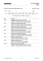
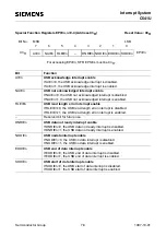
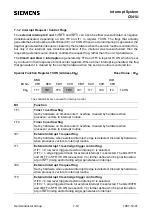
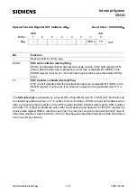
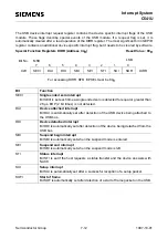
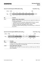
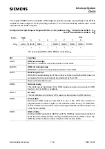
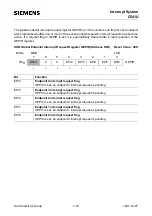
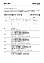
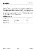
The external interrupts 0 and 1 can be programmed to be level-activated or transition activated by
setting or clearing bit IT0 or IT1 in register TCON. If ITx = 0 (x = 0 or 1), external interrupt x is
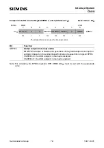
triggered by a detected low level at the INTx pin. In edge-triggered mode (ITx = ) two bits of the
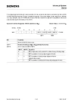
ITCON register define the type of signal transition for which the external interrupt inputs are
sensitive. Edge-triggered interrupt can be activated for an interrupt input signal at the rising edge,
at the falling edge or at both signal transitions. In edge-triggered mode, if successive samples of the
INTx pin show a different logic level in two consequent machine cycles, the corresponding interrupt
request flag IEx in TCON is set. Flag bit IEx=1 then requests the interrupt.
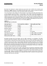
If the external interrupt 0 or 1 is level-activated, the external source has to hold the request active
until the requested interrupt is actually generated. Then it has to deactivate the request before the
interrupt service routine is completed, or else another interrupt will be generated.
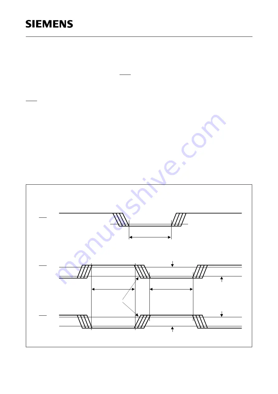
Since the external interrupt pins are sampled once in each machine cycle, an input high or low
should be held for at least 6 oscillator periods to ensure sampling. lf the external interrupt is
transition-activated, the external source has to hold the request pin high for at least one cycle, and
then hold it low for at least one cycle to ensure that the transition is recognized so that the
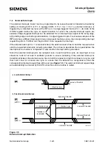
corresponding interrupt request flag will be set (see figure 7-5). The external interrupt request flags
will automatically be cleared by the CPU when the service routine is called.
Figure 7-5
External Interrupt Detection
MCT02577
Level-Activated Interrupt
INTx
Transition-Activated Interrupt
Low-Level Threshold
Transition to
be detected
High-Level Threshold
Low-Level Threshold
b)
a)
INTx
IxETF = 1
=
> 1 Machine Cycle
IxETR = 1
INTx
Low-Level Threshold
High-Level Threshold
> 1 Machine Cycle
> 1 Machine Cycle
Summary of Contents for C541U
Page 1: ... 8 LW 026 0LFURFRQWUROOHU 8VHU V 0DQXDO http www siem ens d Sem iconductor ...
Page 7: ......
Page 21: ...Semiconductor Group 2 6 1997 10 01 Fundamental Structure C541U ...
Page 37: ...Semiconductor Group 4 6 1997 10 01 External Bus Interface C541U ...
Page 133: ...Semiconductor Group 6 88 1999 04 01 On Chip Peripheral Components C541U ...
Page 163: ...Semiconductor Group 8 8 1997 10 01 Fail Safe Mechanisms C541U ...
Page 185: ...Semiconductor Group 10 14 1997 10 01 OTP Memory Operation C541U ...

