background image

– 13 –

SD-CX1W

REMOVING AND REINSTALLING THE MAIN PARTS

MD MECHANISM SECTION

For details about the procedure to remove the MD mechanism
from the main unit, refer to the Disassembly Procedure, Steps
1-8 and 15-18 in the main unit and also the MD section.
(Referring to pages 10 and 12.)

Caution:
After pulling out the optical pickup connector, wrap the end of
the connector in conductive aluminium foil to prevent the
optical pickup from being destroyed by static electricity.

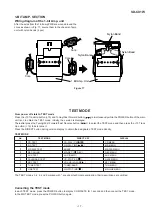
How to remove the magnetic head
(See Fig. 13-1)

1. Remove the screw (A1) x 1 pc.

Caution:
Take utmost care so that the magnetic head is not damaged
when it is mounted.

Figure 13-1

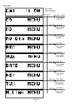
How to remove the MD loading motor PWB/MD
loading motor
(See Fig. 13-2)

1. Remove the screw (B1) x 1 pc.
2. Remove the Hooks (B2) x 3 pcs., and remove the MD

Loading motor PWB.

3. Remove the screws (B3) x 2 pcs., and remove the MD

Loading motor.

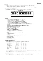
How to remove the MD sled motor/optical pickup
(See Fig. 13-3)

1. Remove the screws (C1) x 3 pcs., and remove the MD

sled motor.

2. Remove the optical pickup.

Caution:
Be careful so that the gear is not damaged.
(The damaged gear emits noise during searching.)

Figure 13-2

Figure 13-3

(C1)x2
ø1.4x4.5mm

(C1)x1

ø1.4x5mm

Optical
Pickup

MD Sled Motor

MD Mechanism
Switch PWB

Washer

MD Mechanism

(A1)x1

ø1.7x5mm

Magnetic Head

Optical Pickup

(B3)x2
ø1.7x3mm

(B1)x1
ø1.7x6mm

MD Loading Motor

MD Loading
Motor PWB

(B2)x2

(B2)x1

Summary of Contents for SD-CX1W(BL)

Page 1: ...ANSISTOR AND LED 35 BLOCK DIAGRAM 36 SCHEMATIC DIAGRAM 40 WIRING SIDE OF P W BOARD 54 WAVEFORMS OF 1 BIT AMP CIRCUIT 67 WAVEFORMS OF MD CIRCUIT 68 WAVEFORMS OF CD CIRCUIT 70 TROUBLESHOOTING 72 FUNCTION TABLE OF IC 81 FL DISPLAY 98 PARTS GUIDE EXPLODED VIEW SERVICE MANUAL SHARP CORPORATION No S3117SDCX1WBL In the interests of user safety the set should be restored to its original condition and only...

Page 2: ...to protect your eyes against exposure to the laser Warning of possible eye damage when repairing If the AC power plug is connected when the inner cover of the unit is removed the laser will light up during focus access about 1 second Fig 2 1 During this operation the laser will leak from the opening between the magnetic head and cartridge holder Fig 2 2 In order to protect your eyes you must not l...

Page 3: ...e parts have already been adjusted prior to shipping 3 No adjustment to the Laser Power should be attempted when replacing or servicing the Pickup 4 Under no circumstances look directly into the Pickup Lens at any time 5 CAUTION Use of controls or adjustments or performance of procedures other than those specified herein may result in hazardous radiation exposure WARNINGS SAFETY PRECAUTION OF CD S...

Page 4: ...erter 1 bit D A converter Frequency response 20 20 000 Hz Dynamic range 90 db 1 kHz MiniDisc Type MiniDisc Recorder Signal readout Non contact 3 beam semiconductor laser pickup Rotation speed 400 900 rpm CLV Approx Eror correction ACIRC Advanced Cross Interleave Reed Solomon Code Quantization 20 bit linear A D converter Coding ATRAC Adaptive TRansform Acoustic Coding ATRAC3 Sampling frequenvy 44 1...

Page 5: ...1 22 23 Multi function LCD display 1 Level Meter Character Information Frequency Indicator 2 Band Selector Indicator 3 Record Indicator 4 CD MD Play Indicator 5 Top Position Indicator 6 Record Mode Indicator 7 MD Record Pause Indicator 8 CD MD Repeat Indicator 9 Surround Indicator 10 Random Play Indicator 11 Programme Play Indicator 12 Sound Synchronised Recording Indicator 13 Track Edit Indicator...

Page 6: ...n 26 Preset Equalizer Button 27 Character Input CD MD Tuner Direct Buttons 28 Display Button 29 Recording Level Cursor Tuner Preset Buttons 30 CD MD Edit Buttons 1 2 3 4 5 6 7 8 9 10 11 12 18 19 20 21 22 23 24 25 26 27 28 29 30 13 14 15 16 17 Buttons with mark in the illustration can be operated on the remote control only Other buttons can be operated both on the main unit and the remote control 1...

Page 7: ...nds Setting the AC voltage selector Check the setting of the AC voltage selector located on the rear panel before plug ging the unit into an AC socket If necessary adjust the selector to correspond to the AC power voltage used in your area Turn the selector with a screwdriver until the appropriate voltage number appears in the window 110 V 127 V 220 V or 230 V 240 V AC Connecting the AC power lead...

Page 8: ...g an optical pickup Re cording and editing are not possible A Shutter will be used on only one side back Recordable MiniDisc This is a raw disc on which recording can be performed A magneto optical disc is used Recordings are made us ing a laser and magnetic field Repeated recording is pos sible Shutters will be used on both sides Recordable Recording prevented Even if the maximum recording time o...

Page 9: ... re cording track numbers Replace it with another record able disc TOC FULL 1 There is no space left for re cording character information Replace it with another record able disc Erase the needless characters MD DISC The data contains an error Press the MD button MiniDisc not specified Replace it with another disc Troubleshooting Chart Many potential problems can be resolved by the owner without c...

Page 10: ...Cable G2 x1 8 MD Unit 1 Screw H1 x4 11 2 9 CD PWB 1 Flat Cable J1 x1 11 3 Note 2 Socket J2 x5 3 Screw J3 x3 10 Switch PWB 1 Screw K1 x1 11 3 11 CD Mechanism 1 Screw L1 x2 11 3 2 Screw L2 x2 12 Display PWB 1 Screw M1 x11 11 4 CD Eject PWB 2 Socket M2 x1 Headphones PWB 3 Hook M3 x2 13 LED PWB 1 Solder Joint N1 x4 11 4 2 Hook N2 x1 14 1 Bit Amp PWB 1 Screw P1 x2 11 5 2 Fan Motor P2 x1 3 Screw P3 x2 4...

Page 11: ... M1 x2 ø3x8mm CD Eject PWB Display PWB Front Panel Headphons PWB N1 x4 LED PWB N2 x1 P1 x2 ø3x6mm P11 x1 ø3x6mm P9 x2 ø3x8mm P6 x1 P4 x1 P2 x1 P10 x1 P11 x1 ø3x6mm P11 x1 ø3x6mm P9 x1 ø3x8mm P11 x1 ø3x6mm P5 x2 ø3x6mm P7 x4 ø3x8mm P3 x2 ø3x6mm P10 x1 P8 x1 P12 x1 P9 x1 ø3x8mm 1 Bit Amp Unit P13 x4 ø3x10mm P14 x1 1 Bit Amp PWB Be careful of the silicon grease J3 x2 ø3x8mm L2 x2 ø3x8mm L1 x2 ø3x20mm...

Page 12: ...igure 12 2 A1 x6 ø4x16mm Net Front Panel Rear Cabinet S1 x2 R2 x1 ø2x2mm R1 x1 ø2x3mm R1 x1 ø2x3mm R1 x1 ø2x3mm R1 x1 ø2x3mm S1 x1 S2 x1 S2 x1 R1 x1 ø2x3mm T1 x2 ø1 7x3mm S3 x1 Q1 x2 ø3x6mm Q1 x2 ø3x6mm Shield Cover Top MD Mechanism Shield Cover Side Shield Cover Bottom MD Main PWB Optical pickup Flexible PWB Note 1 Note 1 After removing the flexible PWB for optical pickup from the connector wrap ...

Page 13: ...magnetic head is not damaged when it is mounted Figure 13 1 How to remove the MD loading motor PWB MD loading motor See Fig 13 2 1 Remove the screw B1 x 1 pc 2 Remove the Hooks B2 x 3 pcs and remove the MD Loading motor PWB 3 Remove the screws B3 x 2 pcs and remove the MD Loading motor HowtoremovetheMDsledmotor opticalpickup See Fig 13 3 1 Remove the screws C1 x 3 pcs and remove the MD sled motor ...

Page 14: ...mbly method on page 10 2 Remove the screws B1 x 4 pcs 3 Remove the CD lid gear unit from the front panel 4 Remove the screws B2 x 5 pcs to remove the gear box B 5 Remove the gear B3 x 1 pc 6 Remove the screws B4 x 2 pcs to remove the CD lid motor How to remove the pickup See Fig 14 2 1 Remove the CD mechanism cover paying attention to the pawls A1 x 4 pcs 2 Remove the screws A2 x 2 pcs to remove t...

Page 15: ...gate driver The level shifted signals are input to the gate driver IC HIP2100 Since the final stage FET array is H bridge two gate drivers are used for 1 CH At this time and of differential signals are input by crossing diagonally for the two gate drivers Positive output to ICA101 ICA103 Hin and ICA102 ICA104 Lin and negative output to ICA102 ICA104 Hin and ICA101 ICA103 Lin Outputofthegatedriverd...

Page 16: ...circuit to be supplied with the power may be defective 2 Excessive output offset of 1 bit amplifier After disconnecting the CNPV99 speaker output connector of 1 bit amplifier turn on the unit power for the normal operation No sound is heard from the speaker After repairing adjust the output offset voltage of 1 bit amplifier as shown on page 22 If the protective operation is observed even after dis...

Page 17: ...elect the TEST mode and then press the 10 Track Up button 10 to determine it Press the DIRECT button during version display to obtain the designated TEST mode directly TEST MODE No TEST MODE DIRECT KEY DISPLAY 1 CD TEST CD PLAY CD CD MENU 2 MD TEST MD PLAY MD MD MENU 3 MD DISP TEST ERASE MD DIS MENU 4 REC AGING MD REC REC REC MENU 5 AUX TEST AUX DEMO AUX MENU 6 CALENDAR TEST CD STOP CD DATE MENU 7...

Page 18: ...ersion display to AUX DEMO Version display to CD STOP Version display to VOL UP Version display to TUNER BAND With SKIP UP button SKIP DWN SKIP UP Version display to CD PLAY Version display to MD STOP SKIP DWN SKIP UP SKIP DWN SKIP UP SKIP DWN SKIP UP SKIP DWN SKIP UP SKIP DWN SKIP UP SKIP DWN SKIP UP SKIP DWN SKIP UP SKIP DWN ...

Page 19: ...switch is turned on 5 MD STOP Automatic adjustment at the present pickup position 6 POWER Canceling the test mode 7 REC MODE To read the coefficient register while the CD operation is stopped To display the error number during CD playback 8 VOLUME UP DOWN Normal volume control 9 CD OPEN CLOSE Normal open close operation Readout of the adjusted value Press the REC MODE button during the stop mode t...

Page 20: ...2 JUMP operation 3 Address setting value up etc TUNING MD SKIP DOWN 1 Forced slide feeding REV 2 JUMP operation 3 Address setting value down etc TUNING VOLUME UP 1 Forced UNLOAD of DISC 2 Set value UP VOLUME DOWN 1 Forced LOAD of DISC 2 Set value DOWN CD STOP 1 To switch laser by EJECT 2 To switch display during continuous playback etc POWER To operation mode without automatic adjustment MD EJECT ...

Page 21: ... OP CL RANDOM CD EJECT FLAG MARK CD PLAY PLAY MARK CD STOP CD SKIP UP TUNING ST SKIP DOWN TUNING STEREO 8 TUNER TEST Outline To test the accurate operation of the tuner The following presets are written a Reception of Preset 1 b Press the POWER button to cancel the TEST mode In this case preset is entirely erased Figure 21 2 TEST MODE MENU PNO Display The flashing display of FM AM AM FM TUN TEST T...

Page 22: ...z P09 1 404 kHz P05 98 00 MHz P10 990 kHz Figure 22 1 AM IF RF GND AM Loop Antenna AM signal oscillator Loop Antenna IF Headphones Frequency cover TP301 Electric Voltmeter UNIT Figure 22 4 Output Offset Lelel Figure 22 2 FM Mute Level Figure 22 3 ADJUSTMENT POINT Preset memory FM frequency AM frequency Preset memory To erase the registered broadcast stations When exiting from the test mode all pre...

Page 23: ... shown at the end of the test mode Although SET was written normally it was not written in the YOBI COMPLETE state Peform AUTO YOBI adjustment After making a normal adjustment write the preliminary adjustment into the EEPROM OK_EEPROM SET and YOBI COMPLETE were written normally WR_EEPROM NG_EEPROM SET could not be written indicate the order of inplementation Checking EEPROM setting EEPROM_SET AUTO...

Page 24: ...utton is pressed the mode is changed If the REC button is pressed instead the mode will change in the opposite order Cancel of test mode The mode is written on EEPROM by pressing the POWER button If the POWER button is pressed again the unit returns to the normal state Before pressing the POWER button make sure that the AUTO pre adjustment AUTO adjustment and AUTO AFB adjustment have been complete...

Page 25: ... Press the MD REC button AUTO pre adjustment menu _ A U T _ Y O B I _ Step 4 Press once the MD PLAY button During automatic adjustment changes as follows _ _ _ _ _ _ HAo TCO End of adjustment If adjustment is OK Step 5 If adjustment is NG Step 6 Step 5 Press the MD STOP button STEP 2 _ C O M P L E T E _ Step 6 Adjustment value output C a n t _ A D J Press the MD STOP button STEP 2 AUTO adjustment ...

Page 26: ...output _ Press the MD STOP button STEP 2 AUTO AFB adjustment Measurement value Step No Setting Method Display Setting value 5 EEPROM setting mode a Focus setting b Spin setting Step No Setting Method Display Step 1 Test mode STOP state t s m e Step 2 Press the CD PLAY button eight times E E P R O M_ S E T Step 3 Press the MD PLAY button _ _ F o c u s _ _ _ Step 4 Press the CD PLAY button _ S p i n...

Page 27: ... 23 Press the CD PLAY button T C R S C 0 L _ Step 24 Press the CD PLAY button T C R S C H h _ Step 25 Press the CD PLAY button T C R S C H L _ Step 26 Press the CD PLAY button C O T L V p _ _ Step 27 Press the CD PLAY button C O T L V r _ _ Step 28 Press the CD PLAY button J P i n t _ _ _ Step 29 Press the CD PLAY button K I K 1 0 _ _ _ Setting value d Sled setting Step No Setting Method Display S...

Page 28: ... _ _ Step 15 Press the CD PLAY button G D E Q B C 2 _ Step 16 Press the CD PLAY button H A L S G _ _ _ Step 17 Press the CD PLAY button L A L S G _ _ _ Step 18 Press the CD PLAY button G A L S G _ _ Step 19 Press the CD PLAY button H A L S O F S _ Step 20 Press the CD PLAY button L A L S O F S _ Step 21 Press the CD PLAY button G A L S O F S _ Step No Setting Method Display Step No Setting Method ...

Page 29: ... _ _ I N N E R _ _ _ Step 3 Press the MD PLAY button INNER switch position measurement s c SUBQ address and C1 error are also indicated Step 4 Press the MD STOP button INNER menu _ _ I N N E R _ _ _ Step No Setting Method Remarks Display Address Whenever the TUNER BAND button is pressed in the address setting mode the address changes as follows 0 0 3 2 0 3 C 0 0 7 0 0 0 8 A 0 0 9 5 0 0 0 3 2 Whene...

Page 30: ... the 3 screws of the spindle motor adjust while observing the Lissajou s waveform 2 After adjustment tighten screws 1 2 and 3 in numerical order See Fig 30 4 Figure 30 4 GND CH1 CH2 X Y 100K 470p 470p a b 100K Osilloscope Lissajous s waveform 4 Pin of IC1201 GND TP1202 11 Pin of IC1201 EIN TP1253 12 Pin of IC1201 FIN TP1254 Less then a b 4 1 Figure 30 1 2 Confirmation Check that the display shows ...

Page 31: ...g MD or hybrid MD DISC FULL No recordable space was found when entering the REC Replace the disc with the one on which the recording PAUSE mode space for UTOC is left PROTECT You tried recording or editing on a disc with the erase Move the tab back to its original position and try prevention tab moved recording or editing again You tried editing the track that is write protected due to the Try edi...

Page 32: ...EJECT 4 Press the TUNER BAND button TEMP Measured temperature Temperature setting 5 Find the temperature correction value for the current ambient temperature on the following table Adjust the temperature correction value using the VOLUME UP DOWN button Ambient Temperature Correction 21 0 C 23 2 C 1 H 23 3 C 26 8 C 0 H 26 9 C 29 0 C 1 H EEPROM DATA LIST Version 01 Focus setting Item indication Sett...

Page 33: ...L K r o i 6 2 H S L K l i o 6 4 H S L K l o i 6 0 H I N N E R 1 8 6 H I N N E R u D 0 H E J _ W A I T 7 8 H C O K 5 8 H F A T C 0 H T A T 3 E H C A T 4 0 H F A B 6 4 H S T R 0 B H S F S 0 D H S T C 0 D H Control setting Item indication Setting C O N T R L 1 0 8 H C O N T R L 2 0 2 H A D J T T M 1 4 H H D E Q A D 9 2 H L D E Q A D 8 E H G D E Q A D 9 1 H G D E Q A D 2 9 1 H M D E Q B C 8 C H L D E ...

Page 34: ...1 no disc System side Until CMD RCV received As quick as possible POWER ON or DISC IN DVDD CN1501 17 18 TRY TRY CN1401 1 2 BACK UP CN1501 4 MD ST TP1800 3 2 V CN1501 7 MCCK IC1401 15 RESET IC1401 12 XRST IC1401 80 RESET CN1501 6 PDOWN CN1501 5 PCONTO CN1501 19 DSTB CN1501 12 DSCK CN1501 8 System side 100 ms 1 5 ms Disc existence Mechanism positioning DISC IN LOADING operation 30 ms 2 ms 3 2 ms 62 ...

Page 35: ... Mylar type P P Polypropylene type NSW802 PICKUP IN ON OFF SW01 CD LID CLOSE ON OFF SW02 CD LID OPEN ON OFF SW601 SPAN SELECTOR 50 9 100 10 SW900 VOLTAGE SELECTOR 230 240 V SW1930 WRITE PRO ON OFF SW1931 DISC MEDIA ON OFF SW1932 LOADING ON OFF SW1933 RECORD ON OFF SW1934 PLAY ON OFF SW1936 LEAD IN ON OFF SWD02 ON STAND BY ON OFF SWD03 MD EJECT ON OFF SWD04 ERASE ON OFF SWD07 CD EJECT ON OFF REF NO...

Page 36: ... QP03 QPO5 MUTING DU01 DISPLAY SECTION DISPLAY SECTION HEADPHONE ALC B6 MD 5V D B8 MD 6V A POWER SECTION 12V A 12V A POWER SECTION ICP01 PRE AMP NJM4558M 1BITAMP SECTION DISPLAY SECTION DISPLAY SECTION VCC VCC B2 B7 CD SECTION TO MD SECTION L CH R CH AUX INPUT TUN_R TUN_L B8 MD 6V A B6 MD 5V D DIG IN D GND POWER MD_RESET MD ST MD_DSCK MD_SERCH MD_KDATA MD_DATA MD_D_STB D GND D GND D GND D GND D VD...

Page 37: ...AY FAN_L M97 FAN MOTOR CNPV97 FAN_L QV87 QV91 QV90 QV88 QV93 QV94 ZD803 ZD802 VF2 VF1 VP B11 D805 D808 B_CONT SP_RELAY M ICV99 KIA4558P OPE AMP ICV98 KIA4558P OPE AMP RLV99 RELAY RL800 RELAY KIA7805AP VOLTAGE REGULATOR VOLTAGE REGULATOR VOLTAGE REGULATOR VOLTAGE REGULATOR VOLTAGE REGULATOR VOLTAGE REGULATOR VOLTAGE REGULATOR VOLTAGE REGULATOR VOLTAGE REGULATOR Q800 D800 F803 T2 5A L 250V F802 T5A ...

Page 38: ... 4 1 2 3 4 5 6 7 1 2 3 4 5 6 7 8 9 33 34 35 36 37 38 39 40 41 42 43 44 45 46 47 48 17 18 19 20 21 22 23 24 25 26 27 28 29 30 31 32 16 15 14 13 12 11 10 9 8 7 6 5 4 3 2 1 1 2 3 4 5 D_OUT DATA BCK LRCK D_3R3V CD_FUNC DR_CL_IN DR_OP_IN DR_M DR_M CD_FUNC PU_IN DR_M DR_CL_IN DR_M DR_OP_IN A_3R3V A_3R3V BUS0_ BUS1_ BUS2_ BUS3_ BUCK_ CCE_ 7R2V_CD 7R2V_CD CD_RES TO MAIN SECTION VO3 VO3 VO5 VO5 VO4 VO4 P G...

Page 39: ...IC1202 IX2474AF 4M BIT DRAM 5 9 11 15 26 29 32 36 42 IC1201 LR37816A ENDEC ATRAC XL1201 33 8688MHz IC1101 IR3R58M RF SIGNAL PROCESSOR 3 2V 3 2V MECHANISM 4 75 5 25V E F SIGNAL A B SIGNAL RF1 RF4 SIGNAL IC1601 M56788FP MOTOR DRIVER 12 10 15 M M903 MD LOADING MOTOR SW1932 LOADING SW1934 PLAY SW1936 LEAD IN MONITOR DIODE LASER DIODE RF4 RF3 RF2 RF1 LIGHT RECEIVING SECTION ERROR SIGNAL LIGHT RECEIVING...

Page 40: ...12 20 19 18 17 16 15 14 13 21 22 24 23 2 1 3 MAIN PWB A1 0V 0V 0V 4 2V 4 2V 4 2V 4 2V 4 2V 4 2V 4 2V 4 2V 4 2V 4 2V 4 2V 4 2V 4 2V 4 2V 4 2V 4 2V 4 2V 4 2V 8 4V 4 8V 11 1V 11 4V 11 1V 0V 0V 11 1V 2 2V 2 9V 2 9V 1 30 1 2 3 4 5 6 7 8 9 10 TO MD PWB CN1501 P53 12 G SURROUND ON OFF SURROUND MUTING 4 2V B B B B B B B B B B CNP603 B B P48 1 B ICU01 LC75341M CNS302 P43 12 H CW1501 28 FWM01 CU35 100P CH C...

Page 41: ...00K CS04 0 0047 QU01 KTC3199 GR QP02 KTC3199 GR CP02 2 2 50 RS25 10K RS26 10K RP08 4 7K RP07 4 7K CS08 0 22 50 RS08 100K CP13 47 25 RP27 47 RP13 6 8K CP33 100 16 CP01 2 2 50 RS23 100K RS24 100K RP03 4 7K RP02 22K RP01 22K CP09 2 2 50 CP10 2 2 50 RP05 100K CP07 1 50 CP08 1 50 CP14 47 25 RP04 4 7K RP06 100K CP05 100P CH ICP01 PRE AMP NJM4565M CP06 100P CH RP28 47 RP11 1K RP12 1K CNPP01 CU41 0 0022 D...

Page 42: ...COVERAGE GND FM IF 10 7MHz C324 0 47 50 C339 100P CH R323 68K C334 18P UJ C337 0 022 T306 C335 330P C323 0 022 T302 R336 10K C330 15P UJ C338 0 0022 VD301 SVC348S VR351 10 K B R386 1K C342 0 022 L353 1mH C332 0 022 C331 0 047 R358 8 2K C343 33P CH T CF302 C352 10 16 C351 0 022 R351 5 6K C361 0 022 C362 3 3 50 C350 0 047 C310 100P CH C384 0 001 C394 47 25 R380 1 5K C392 0 001 C393 1 50 R381 10K L34...

Page 43: ...ND TUN R CNPU03 P40 3 H TO MAIN PWB 10 9 8 7 6 5 4 3 2 1 B CNS302 10 9 8 7 6 5 4 3 2 1 CF352 C372 1 50 C371 1 50 C373 0 022 R357 470K C374 0 022 C343 33P CH R352 1K T351 C358 1 50 CF351 FM IF R356 1K C368 1 50 C366 0 001 R353 270 C354 0 022 C353 0 022 C399 0 022 C398 100 10 C356 0 001 C357 2 2 50 C361 0 022 C362 3 3 50 C364 10 16 C363 0 022 C365 0 022 C367 1 50 R350 2 7K X351 456kHz C350 0 047 C37...

Page 44: ...1 7V 1 65V 1 65V 0V 0V 3 7V 3 2V 3 2V 3 2V 3 2V 0V 7 2V 3 3V 7 2V 1 65V 1 65V 0V 0V 5V 3 7V 1 65V 1 65V 1 65V 1 65V 0V 2 67V 0V 3 3V 1 75V 1 65V 1 65V 0 6V 1 62V 1 23V 1 65V 0 75V 1 65V 1 65V 1 65V 2 1V 0V 1 65V 1 1V 2 39V 6 17V 1 96V 1 96V 1 96V 1 96V 3 54V 3 54V 0V 1 2 LASER DRIVER SWITCHING REGULATER SWITCHING B B B B B 1 8 3 2 6 5 IC1 IC2 12 11 4 13 CNP102 TO POWER PWB P48 1 D R74 2 2K NC NC N...

Page 45: ...V 0V 1 2V 0V 1 65V 0V 0V 1 57V 1 65V 3 3V 1 65V 0V 0 76V 1 65V 0 64V 1 65V 1 65V 1 65V 1 65V 1 65V 1 54V 1 75V 0V 3 3V 1 65V 1 65V 0V 3 3V 0V 0V 1 51V 1 55V 3 3V 0V 1 65V 3 3V 1 65V 1 65V 0V 4 81V 0V 4 74V 4 63V 4 62V 4 58V 4 62V 4 45V 4 81V 4 81V 57 58 59 60 61 62 63 64 P41 12 G 18 1 TO DISPLAY PWB FWD03 P53 12 E P47 12 B B B B B 10 9 7 IC3 Synchronizing signal guarantee EFM demodulation Address ...

Page 46: ...V KEY 3 KEY 2 KEY 1 POWER SPAN CD_OP CL_SENS TUNER_SM PROTECT H P_SW MD_RESET MD_ST MD_LOADSW_ MD_SERCH MD_D_STB MD_DSCK 3 1 5 4 2 3 1 5 4 2 3 1 5 4 2 D1 S16 S20 S19 S28 S27 S26 S25 D0 D3 D2 S31 S30 S29 S24 S23 S22 S21 S18 S17 S11 S21 S20 S19 S18 S17 S16 S15 S14 S13 S12 S10 S9 S8 S7 S6 S5 S4 S3 S2 S1 S0 79 1 3 2 1 3 2 2 1 3 LED8 LED9 LED10 LED11 4 9V 0V 0 2V 5 8V 5 8V 5 8V 0V 0V 0V 4 3V 4 8V 4 8V ...

Page 47: ...V DIG1 20V DIG0 20V 17 18 19 20 21 22 23 24 25 26 27 28 29 30 31 32 33 34 35 36 37 38 39 40 41 42 43 44 45 46 47 48 49 50 64 63 62 61 60 59 58 57 56 55 54 53 52 51 51 MD_RESET _ MD_D_STB MD_DSCK MD_KDATA MD_DATA_ BUS0 BUS1 BUCK CCE BUS2 BUS3 MD_D_STB_ MD_D_STB MD_DATA MD_DATA_ 3 2 1 REMO RESET SYS_STOP DI CLK DQ CE TO POWER PWB D8 D6 D1 D7 D12 D11 D10 D9 D5 D4 D3 D2 D13 2 1 3 2 3 1 2 3 1 2 3 1 3 1...

Page 48: ... 4 3 3 2 1 3 2 1 3 2 1 3 2 1 3 2 1 3 2 1 B_CONT 12V_M 12V_A 12V A 3 2 1 4 1 4 1 FROM 1 BIT AMP PWB 0V 0 7V 5 6V 11 4V 0 7V 12V 0V 17V 7 3V 1 3V 12V 0V 12 4V 22V 11 7V 5V 0V 33 8V 34 3V B FROM 1 BIT AMP PWB FROM 1 BIT AMP PWB D826 DS1SS133 R825 330 R826 330 D810 DS1SS133 D815 DS1SS133 D814 DS1SS133 IC804 KIA7805AP C832 0 022 C831 1 50 R817 150 Q802 KTA1271 Y C830 47 25 IC803 KIA7812AP ZD804 DZ13BSA...

Page 49: ...V98 DZ6 2BSA QV91 KTC3203 Y RV48 10K RV56 10K QV92 KTC3199 GR RV57 100K RV58 4 7K QV93 KRC107 M QV94 KRC107 M QV87 KTC3199 GR RV51 100K CV73 47 25 CV72 47 25 RV54 120K RV53 4 7K DV87 DS1SS133 DV88 DS1SS133 RV59 22K RV60 22K CV96 0 0022 RV89 180K RV68 100K RV80 5 6K RV81 5 6K RV76 180K CV90 0 0022 DV92 DS1SS133 QV99 KTC3199 GR RV67 10K RV71 390 CV79 47 25 CV78 0 022 RV72 10K RV70 1 2K CV77 0 01 RV6...

Page 50: ...101 2 2K CA 0 DA109 1SS362 DA108 1SS362 CA152 12P CH RA112 2 2K DA100 KDS160 CA153 18P CH RA113 2 2K CA154 18P CH RA114 2 2K CA155 12P CH RA115 2 2K DA128 1SS361 DA127 1SS361 DA129 1SS361 DA126 1SS361 ICA110 QUAD 2 INPUT AND GATE TC74AC8T CA110 0 1 DA102 KDS160 DA101 KDS160 DA103 KDS160 CA212 100 16 CA213 100 25 DA130 KDS160 CA111 330 6 3 CA198 0 1 CA131 0 22 CA128 0 22 CA121 0 22 CA118 0 22 RA116...

Page 51: ...56 DA117 SFPW56 DA116 SFPW56 QA101 SLA5001 DA114 SFPW56 DA115 SFPW56 QA100 SLA5001 DA113 SFPW56 RA339 47K CA214 0 001 RA126 2 2K RA125 2 2K RA337 10 RA336 10 RA338 10 RA335 10 RA333 10 RA332 10 RA331 10 RA334 10 CA132 1 0 50 CA193 0 001 RA327 10 RA326 10 RA325 10 RA328 10 RA323 10 RA322 10 RA321 10 RA324 10 RA315 10 RA316 10 RA318 10 RA317 10 CA124 1 0 50 CA122 1 0 50 RA306 10 RA305 10 RA307 10 RA...

Page 52: ... 5 4 3 2 1 APCIN LDON LDVCC DGND B LVVOUT F COIL T COIL I V I V I V I V SW APCOUT DGND LDVAR A COM RF1 F E RF2 RF4 VCC MP R RF3 T F AGND F T DGND EXT C LDOUT APC LVV LDON GND VCC LVVIN 2 8V MD PICKUP UNIT LDVAR FLEXIBLE PWB TP1971 TP1972 TP1975 TP1974 TP1973 TP1945 TP1944 TP1946 TP1943 TP1941 TP1942 LEAD IN LD LD MINF LOADING GND M MD MECHANISM SWITCH PWB F1 MD LOADING MOTOR PWB F2 1 3 3 2 1 2 MD ...

Page 53: ...A0 RAA1 RAA6 RAA9 RAD3 RAWEX XI LRCK BCLK RSTX SYD0 SYD1 SYD2 SYD3 SYD4 SYWRX VBAT FIN EIN BIN AIN X176KO TEST2 1 1 1 1 1 3 3 3 2 2 2 3 3 2 2 2 3 1 CNPU04 P40 5 H TO MAIN PWB CNP8 P45 12 B TO CD PWB MD SIGNAL 1 2 3 4 1 2 3 4 1 28 1 28 CD SIGNAL PLAYBACK SIGNAL RECORD SIGNAL NC NC NC NC HIGH DISC 0V 0V 3 2V 3 2V 3 2V 0V 0V 0 1V 0V 0V 0V 0V 0 2V 0V NC NC NC NC NC 0V 0V 0V 0V 0V 0V 3 2V 3 2V 0V 3 2V ...

Page 54: ...1W 54 A B C D E F G H 1 2 3 4 5 6 Figure 54 WIRING SIDE OF P W BOARD 1 13 MAIN PWB A1 TOP VIEW BR COLOR TABLE RD R OR YL GR BL VL GY WH W BK PK BROWN RED ORANGE YELLOW GREEN BLUE VIOLET GRAY WHITE BLACK PINK ...

Page 55: ...01 CP04 RP05 RP11 RP06 RP12 RP17 RP13 CP06 RP02 RP04 RP15 RP31 RP16 RP14 RP18 RS24 RS26 CU19 RS08 RP08 RU01 RP07 CS04 RU12 RU07 RS14 RS12 CS06 RS04 RS02 RU32 RS17 CU36 RU31 CU13 CU35 CU34 RU11 RU09 RU21 CU48 CU49 CU42 RU19 RU70 CU41 RU61 CU50 RU22 RU40 CU31 RU30 RU10 ICU01 CU14 RU02 RU08 CU20 RP20 RP24 RP19 RP23 RU05 RU06 CU06 FROM TUNER PWB 10 1 1 3 5 7 9 11 13 15 17 19 21 23 25 27 29 2 4 6 8 10 ...

Page 56: ...SD CX1W 56 Figure 56 WIRING SIDE OF P W BOARD 3 13 A B C D E F G H 1 2 3 4 5 6 TUNER PWB A2 TOP VIEW ...

Page 57: ...351 C363 C361 R370 C356 R384 C355 R385 R383 R395 C343 R376 R358 R360 R393 R371 R378 C312 R372 R345 C341 C345 C387 C311 R379 R373 C310 R374 R380 C392 R381 C397 C381 C382 R323 R336 C390 C346 C347 C332 C339 C335 C337 R386 C342 C354 C377 R389 R359 R399 C395 C389 L353 1 2 3 4 5 6 7 8 9 10 TO MAIN PWB TUNER PWB A2 BOTTOM VIEW AM GND FM 8 7 6 5 4 3 2 1 1 2 3 4 5 6 7 8 9 10 11 12 13 14 15 16 17 18 19 20 2...

Page 58: ...NG SIDE OF P W BOARD 5 13 A B C D E F G H 1 2 3 4 5 6 CD PWB A3 TOP VIEW PICKUP UNIT 8 7 6 5 4 3 2 1 7 6 5 4 3 2 1 BR COLOR TABLE RD R OR YL GR BL VL GY WH W BK PK BROWN RED ORANGE YELLOW GREEN BLUE VIOLET GRAY WHITE BLACK PINK ...

Page 59: ...7 R46 R45 R64 R60 R68 C41 C40 R67 C37 C44 C39 C66 R31 C9 C36 R65 C5 C38 C35 C43 R66 R9 C34 C74 R10 C73 C11 C21 C33 C25 R12 R11 R20 R19 IC2 C22 R18 C14 R17 R16 C16 R14 C15 R5 R6 C1 R4 R3 R2 R1 18 16 14 12 10 8 6 4 2 17 15 13 11 9 7 5 3 1 CD PWB A3 BOTTOM VIEW 1 1 1 2 1 2 2 3 4 5 6 6 RD GY GY GY GY BK GY GY CD MOTOR PWB D 18 18 1 1 FWD03 TO DISPLAY PWB 1 2 3 1 8 RD GY GY GY GY GY GY GY RD GY GY GY G...

Page 60: ... C822 IC802 D814 C841 D815 C824 IC803 C826 C828 IC804 C831 C833 D800 C807 C801 C800 BI02 BI02 R802 R801 R800 R817 R807 C838 C835 RV59 CV92 RV60 RV55 CV96 RV49 CV95 RV66 RV54 RV51 RV65 RV57 RV58 RV72 RV70 RV71 CV80 RV68 CV78 CV88 CV77 CV93 R823 R819 R820 R811 R815 C820 C823 C827 C832 1 1 4 4 1 3 1 5 7 9 4 2 6 8 10 11 13 15 17 19 21 3 1 5 7 9 11 13 15 17 19 21 23 12 14 16 18 21 22 4 2 6 8 10 12 14 1...

Page 61: ... OR YL GR BL VL GY WH W BK PK BROWN RED ORANGE YELLOW GREEN BLUE VIOLET GRAY WHITE BLACK PINK F803 T2 5A L 250V T F T901 MAIN POWER TRANSFORMER F802 T5A L 250V F801 T5A L 250V T900 SUB POWER TRANSFORMER SO900 AC POWER INPUT SOCKET AC 110 127 220 230 240 V 50 60 Hz B C E ZD900 Q901 B C E R905 R903 R904 ZD901 F901 T2A L 250V 3 4 5 SW900 VOLTAGE SELECTOR 110V 127V 220V 230 240V OR YL 5 WH 110V 127V 2...

Page 62: ... CA120 CA117 RA165 ICA101 RA169 RA166 CA116 RA168 CA119 CA118 RA167 RA170 RA120 DA107 CA112 CA115 DA106 ICA110 CA113 CA114 RA119 RA202 RA108 CA104 ICA100 CA126 RA172 CA131 CA129 RA171 ICA104 CA127 CA130 CA193 CA134 LA106 CA128 ICA103 ICA102 CA121 LA104 1 BIT AMP PWB C TOP VIEW 1 4 5 8 1 4 5 8 1 5 7 8 10 14 1 5 10 12 13 15 20 24 1 4 5 8 1 4 5 8 10 9 3 4 5 6 2 1 ...

Page 63: ... RA325 RA334 RA331 RA179 RA180 ZDA110 DA128 DA127 RA175 RA178 RA176 RA177 DA129 DA126 RA100 RA173 RA101 RA174 RA184 CA214 CA211 RA183 RA154 RA342 QA103 ZDA111 LA130 CA223 CA142 CA143 BIA110 CNSA110 LFA04 LFA03 RA341 RA340 CA224 LFA05 CA159 CA163 CA160 LFA06 BIA111 CNSA111 CNP801 CA162 CA150 LA131 LA133 CA151 VRA100 CA212 CA184 CA106 CXA100 CA105 CA186 CA108 LA124 CA109 CA165 CA164 CA194 BIA106 CA1...

Page 64: ... 35 40 45 50 51 55 60 65 70 75 80 81 85 90 95 100 1 5 10 14 15 20 25 28 1 3 4 5 1 4 5 8 1 2 3 R1538 R1537 R1536 R1535 R1534 R1533 R1532 R1510 CK3 TP1122 TP1123 TP1121 TP1120 TP1630 TP1607 CK2 TP1603 TP1600 TP1400 TP1210 TP1205 TP1208 TP1206 TP1214 TP1601 TP1213 TP1203 TP1116 TP1136 TP1131 TP1107 TP1108 TP1115 TP1110 TP1111 TP1130 TP1109 TP1106 TP1102 TP1105 TP1117 TP1100 TP1101 TP1135 TP1104 TP111...

Page 65: ...4 Q1807 C1409 R1443 R1401 R1435 R1440 R1420 R1403 D1402 C1706 L1554 R1407 R1424 R1405 Q1403 Q1806 Q1803 R1805 Q1805 R1808 C1303 R1801 Q1801 R1614 R1612 Q1501 C1802 D1401 Q1800 R1806 Q1802 Q1402 R1802 R1803 C1606 C1304 C1302 R1304 L1300 R1704 IC1702 C1707 Q1702 Q1700 C1503 C1506 C1509 R1516 R1513 L1552 R1561 L1551 C1714 R1511 R1515 C1710 C1712 C1501 R1716 R1714 R1711 R1712 Q1701 R1708 C1711 C1716 R...

Page 66: ...48 CD49 RE37 CD46 CD47 RD78 RE35 RE46 RE31 RE29 RE30 CD17 RE42 RE43 CD18 RE40 RD23 RD39 CD23 CD22 CD21 ICD01 CD06 RE12 RE11 RE10 RE09 RE08 RE07 RE06 RE05 RE04 RE03 RE02 RD44 RD43 RE50 RD51 CD35 CD34 CD33 CD32 CD19 RD56 CD45 LEDD07 LEDD08 LEDD10 1 22 22 1 CNP601 TO POWER PWB FWD03 18 1 1 18 1 3 5 7 9 11 13 15 17 19 21 2 4 6 8 10 12 14 16 18 20 22 1 3 5 7 9 11 13 15 17 2 4 6 8 10 12 14 16 18 CNPD1 T...

Page 67: ...ence side 5 V amplitude is observed at 2 V negative supply voltage corresponding to VINH and VINL of gate driver during 9 V operation Approx 0 8 VCC and 0 2 VSS 7 8 FET is based on the negative supply voltage the gate voltage of the LOW side FET operates with the negative power and 9 V To make HIGH SIDE FET completely on the positive supply voltage of 4 5 V or over is required At the bootstrap the...

Page 68: ...sc STOP PLAY TP1518 RESET TP1800 3 2V TP1511 PCONT0 TP1212 FEMON TP1422 DSENSE TP1420 FOK TP1201 EFMMON TP1135 ADIPO TP1122 F TP1207 TEMON TP1603 SP TP1602 SP TP1122 F TP1122 F TP1207 TEMON TP1603 SP TP1602 SP 1 2 3 4 4 6 10 11 4 6 10 11 4 5 12 13 14 15 5 6 7 4 5 6 7 4 6 8 9 4 6 8 9 TP1122 F TP1212 FEMON TP1207 TEMON TP1451 ADJUST TP1122 F TP1212 FEMON TP1207 TEMON TP1451 ADJUST TP1122 F TP1207 TE...

Page 69: ...EMON TP1121 T TP1421 CIN TP1121 T TP1421 CIN 72 IC1201 DFCK 72 IC1201 DFCK TP1300 REC HEAD TP1302 EFMO TP1105 LDVAL TP1113 R P 71 IC1201 BCLK 3 IC1202 WE 17 IC1202 CAS 1 IC1202 I 01 6 IC1202 A0 70 IC1201 LRCK 74 IC1201 DADATA 71 IC1201 BCLK 70 IC1201 LRCK 73 IC1201 ADDATA PLAY Low reflection disc PLAY High reflection disc 14 28 29 30 31 18 32 20 21 33 34 35 36 6 16 17 14 6 16 17 18 19 20 21 22 23 ...

Page 70: ...ack jump CH1 1 During the tracking jump TEO RFRP 2 IC2 11pin IC2 17pin T IC2 15 pin IC1 4 pin IC1 3 pin Stopped CH1 500mV 2000 09 18 15 29 21 DC 10 1 CH2 2V DC 10 1 CH3 2V DC 10 1 2ms div 2ms div NORM 500kS s 1 2 3 Record Length Smoothing ON CH1 0 000V CH2 0 00V Main 10K Zoom 5K Mode SINGLE Type EDGE CH2 Delay 102 3ns Hold off MINIMUM CH3 0 00V CH4 0 00V BW 20MHz Trigger Filter CH1 CH3 CH4 EXT LIN...

Page 71: ...20MHz Trigger Filter Offset T CD test 2 3 upgrade 1div CH Position To 3div 1div 0div 3div CH3 Position 3 00div 7 Disc motor output while in the test mode 11 12 DMO SP SP Stopped When there is no wound in the disk CH1 1V 2000 09 18 17 16 55 CH1 V DIV 1V 500us div 500us div CH1 V DIV CAL Smoothing ON BW 20MHz CH1 0 00V CH2 0 00V Main 10K Zoom 4K CH3 0 00V CH4 0 00V Mode AUTO Type EDGE CH1 Delay 102 ...

Page 72: ... lens during use and it may degrade performance To avoid this problem use a cleaning disc designed for CD optical pickup lenses HOW TO USE CAUTION Cleaning fluid Cleaner disc Using the brush in the cleaner cap apply 1 or 2 drops of the cleaning fluid to the brush on the CD cleaner disc which has the mark next to it Place the CD cleaner disc onto the CD disc tray with the brush side down then press...

Page 73: ...n the main unit Refer to The laser does not light up Is the output at pin 19 HF of IC2 flat in the CD test mode 4 Does the sled motor run Refer to Track search is impossible No Aretracksplayedfromthetrack1inascendingorderbypressing the button Refer to The disc motor CLV servo is defective Refer to The sled motor does not run No Refer to No sound is heard Yes When the unit is turned off and on agai...

Page 74: ...ode 4 No Check the parts around IC1 If OK IC1 is defective Is there the output between pins 5 and 6 on IC1 Yes Yes Is the output tracking error signal found at pins 4 and 5 on IC2 in the CD test mode 3 Abnormal Yes No Refer to The sled motor does not run IC2 is defective Check the portion between IC1 and CNS2 and connection of the optical pickup wires If OK the optical pickup is defective Check th...

Page 75: ...ate in the CD test mode 3 No Yes Does the disc motor rotate too rapidly or slowly Yes Recheck whether the optical pickup objective is dirty If it is dirty clean it Check the connection between pin 19 on IC2 and pin 24 on IC3 If OK the optical pickup is defective No Does the eye pattern appear at pin 19 on IC2 Refer to the waveform diagrams on page 70 It is OK even if the waveform is not clear IC3 ...

Page 76: ... outputted from pins 3 6 and 11 AOUT of IC4 No Check the CD MD connection sections Is the digital signal sent to pins 25 26 and 27 of CN1501 on the MD PWB Yes Is the digital signal outputted from pins 1 2 and 3 AOUT of IC3 No OK Yes No Check the connection of parts around IC3 If OK IC3 is defective Check the connection between pin 20 of IC1 and pin 40 of IC3 If OK C1 is defective Yes The sled moto...

Page 77: ...m Record and playback operations No Yes Playback state cannot be set Is it impossible to set both high reflection disc and low reflection disc to playback state No Check as stated in item TEST mode check Yes Only the high reflection disc cannot be played back Yes Is 1 3 V to 1 6 V applied to the pin 93 of IC1401 with the high reflection disc inserted Only the low reflection disc cannot be played b...

Page 78: ... Yes Disc retracts soon after completion of disc ejection Yes Check SW1932 Is the pin 5 of CN1401 set to H state Yes No Check the main PWB and CN1501 No Check the power PWB main PWB and CN1501 Is pulse input in the pin 6 of CN1501 when reset power supply is turned on Is 5 V to 6 V applied to the pins 17 and 18 of CN1501 Yes No Check IC1201 No Check the periphery of Q1804 and IC1401 Is pulse of 8 4...

Page 79: ...the normal mode playback set the record playback TEST mode Is recording performed after displaying TEST REC Yes No Check whether the disc is record prohibited Is RF waveform output to the pin 1 of IC1201 or TP1201 when playback is performed after recording No Does RF pattern appear on the pin 50 of IC1201 during recording Yes No No Check for IC1201 soldering failure Yes Is output waveform given to...

Page 80: ...tor and for disconnection Yes Replace the sled motor The spindle motor does not rotate Is waveform output from the pins 25 of IC1201 in the step 4 of AUTO auxiliary adjustment mode of TEST mode Check IC1601 CN1401 and soldering of mechanism switch PWB Is waveform output from the pins 9 and 10 of IC1601 and the pins 4 and 5 of CN1401 Replace with a spindle motor complete No No Yes Yes Check the pin...

Page 81: ...rsion input terminal for PLL system low pass filter 19 LPFO Output Amp s output terminal for PLL system low pass filter 20 PVREF Input VREF terminal only for PLL system 21 VCOF Output Filter terminal for VCO 22 AVSS3 Analog GND terminal 23 SLCO Output DAC output terminal for data slice level generation 24 RFI Input RF signal input terminal Zin can be selected by command 25 AVDD3 Input Analog 3 3 V...

Page 82: ...E Input Chip enable signal input terminal for microcomputer interface In case of L BUS3 0 are active 63 RST Input Reset signal input terminal Reset L 64 VDD5 Input 5 V power supply terminal for microcomputer interface Pin No Terminal Name Function Input Output In this unit the terminal with asterisk mark is open terminal which is not connected to the outside Note AI F Analog input output terminal ...

Page 83: ...n terminal 20 RBASS Bass band filter capacitor and resistor connection terminal 21 ROUT Bass band filter capacitor resistor connection terminal and bass treble output terminal 22 Vref 0 5 VDD voltage generation section for analog ground Connect a capacitor of 10 µF or more between Vref and AVSS VSS as a countermeasure against the power supply ripple 23 VDD Power supply terminal 24 CL Serial data a...

Page 84: ...terminal 18 Rch Vref Input Reference voltage terminal for R channel 19 Lch Vref Input Reference voltage terminal for L channel 20 Lch IN Input L channel analog input terminal 21 RESET Input Reset terminal It is reset with L 22 NFL2 Input L channel reverse signal feedback input terminal 23 NFL1 Input L channel forward signal feedback input terminal 24 VDDA Input Analog current terminal for AD conve...

Page 85: ... 20 P66 SCLK11 MD_D_SCK Output MD clock output 21 P65 SOUT1 MD_KDATA Output MD KEY data 22 P64 SIN1 MD_DATA Input MD data input 23 P63 CNTR1 CD_BUS3 Input Output Data input output terminal for CD interface 3 L output fixed except CD function 24 P62 CNTR0 CD_BUS2 Input Output Data input output terminal for CD interface 2 L output fixed except CD function 25 P61 PWM CD_BUS1 Input Output Data input o...

Page 86: ... 72 P37 SEG31 P30 SEG24 SEG32 SEG25 Output Segment output for FL No 32 No 25 73 80 P97 SEG23 P90 SEG16 SEG24 SEG17 Output Segment output for FL No 24 No 17 81 88 P87 SEG15 P80 SEG08 SEG16 SEG9 Output Segment output for FL No 16 No 9 89 90 PA7 SEG07 PA6 SEG06 SEG8 SEG7 Output Segment output for FL No 8 No 7 91 VCC VCC Input Power supply 5 V 92 97 PA5 SEG05 PA0 SEG00 SEG6 SEG1 Output Segment output ...

Page 87: ...EY1 KEY2 KEY3 P_DOWN TUNER_SM PROTECT SPAN POWER H P_SW CD_OP CL_SENS MD_LOAD_SW MD_ST MD_SERACH MD_RESET MD_D_STB MD_D_SCK MD_KDATA MD_DATA CD_BUS3 CD_BUS2 CD_BUS1 CD_BUS0 CD_BUSK CD_CCE AVSS VREF VEE PA0 SEG0 PA1 SEG1 PA2 SEG2 PA3 SEG3 PA4 SEG4 PA5 SEG5 VCC PA6 SEG6 PA7 SEG7 P80 SEG8 P81 SEG9 P82 SEG10 P83 SEG11 P84 SEG12 P85 SEG13 P86 SEG14 P87 SEG15 AVSS VREF VEE SEG1 SEG2 SEG3 SEG4 SEG5 SEG6 ...

Page 88: ...l for track count 18 RFRPIN Input Signal generation amp input terminal for track count 19 RFGO Output RF signal amplitude adjustment amp output terminal 20 RFGC Input RF amplitude adjustment control signal input terminal RFGC input voltage 21 AGCIN Input RF signal amplitude adjustment amp input terminal 22 RFO Output RF signal generation amp output terminal 23 RFN Input RF signal generation amp in...

Page 89: ...tem power supply 24 P GND2 Power system GND CH1 2 6 25 V01 CH1 output Inversion against input 26 V01 CH1 output Non inversion against input 27 V02 CH2 output Inversion against input 28 V01 CH2 output Non inversion against input 29 V06 CH6 output 20 V06 CH6 output Figure 89 BLOCK DIAGRAM OF IC In this unit the terminal with asterisk mark is open terminal which is not connected to the outside VO3 VO...

Page 90: ...vo focus servo system 22 TCGO Group mode Track cross detection signal amplifier output terminal 23 TCGI Group mode Track cross detection signal amplifier input terminal 24 RFADD Resistance addition output terminal of RF1 RF4 25 DTEMP Chip temperature detection terminal 26 SGAIN Switch section control terminal of amplifier for servo 27 DISC Pit mode groove mode selecting control terminal 28 OPICPW ...

Page 91: ...8 89 90 91 92 93 94 95 96 97 98 99 100 50 49 48 47 46 45 44 43 42 41 40 39 38 37 36 35 34 33 32 31 30 29 28 27 26 TOTMON TEMCN SBCK SBO SBSY SFSY FCK SENSE COUT MCCK DINIX VDD2 DGND RSTX SYD0 SYD1 SYD2 SYD3 SYD4 SYD5 SYD6 SYD7 SYWRX SYRDX SYRS EFMO PLCK ACRCEF RAA11 RAD0 RAD1 RAWEX RARASX RAA9 RAD3 RAD2 RACASX DGND RACEX RAA8 RAA7 RAA6 RAA5 RAA4 VDD2 RAA10 RAA0 RAA1 RAA2 RAA3 EFMMON AVCC1 EFM1 AGN...

Page 92: ...tput to external D RAM ADR0 LSB 30 RAA10 Output Address output to external D RAM ADR10 MSB 31 VDD2 Input Power supply for interface 32 RAA4 Output Address output to external D RAM ADR4 33 RAA5 Output Address output to external D RAM ADR5 34 RAA6 Output Address output to external D RAM ADR6 35 RAA7 Output Address output to external D RAM ADR7 36 RAA8 Output Address output to external D RAM ADR8 37 ...

Page 93: ...or output Series resistance 10 100 kΩ built in 77 TEMON Output Tracking error signal monitor output Series resistance 10 100 kΩ built in 78 SBCK Input Output DIN subcode read clock Expansion port 4 79 SBO Output DIN subcode serial data Expansion port 5 80 SBSY Output DIN subcode block synchronous signal Expansion port 6 81 SFSY Output DIN subcode frame synchronous signal Expansion port 7 82 FOK Ou...

Page 94: ... A0 A2 Device address 4 VSS Ground 5 SDA Serial data input output 6 SCL Serial clock input 7 WP Write protect 8 VCC Power supply Figure 94 1 BLOCK DIAGRAM OF IC Figure 94 2 BLOCK DIAGRAM OF IC Figure 94 3 BLOCK DIAGRAM OF IC Figure 94 4 BLOCK DIAGRAM OF IC 4 RAS 5 17 15 CAS A0 A9 WE DQ0 20 VSS VBB 17 CAS Clock Generator CBR Refresh Counter Row Address Buffer Memory Cell I O Selection Write Clock G...

Page 95: ...release output 28 HFON Output HFON 29 EEPK Output EEPROM serial clock output 30 EEPD Input Output EEPROM data input output 31 MD DATA Output MD computer data input output 32 K DATA Input System computer data input 33 DSCK Input System computer clock input 34 DSTB Output DSTB system computer communication possible and during communication 35 N C Output Not used 36 SBO Input Subcode serial data inpu...

Page 96: ...t output port P24 69 P23 Output Input output port P23 70 PCNT0 Output PCNT0 output 71 LAST Output LAST 72 LD ON Output LDON output H ON 73 A B Input ANLPTR output ADC DAC selection input 74 SBSY Input Subcode communication block synchro input 75 DAP ON Output DAPON output for CK 76 DFS0 Output DFS0 output 77 DFS1 Output DFS1 output 78 P12 Input Input output port P12 79 P11 Input Input output port ...

Page 97: ...control 2 Pulled down 22 VSSA DAC DA converter analog ground 23 VDDA ADC DA converter analog power 24 VOUTR DA converter output right 25 VDDO Opeamp power 26 VOUTL DA converter output left 27 VSSO Opeamp ground 28 Vref D AD converter reference voltage IC1701 VHiUDA1345 1 AD DA Converter UDA1345 Pin No Function Terminal Name In this unit the terminal with asterisk mark is open terminal which is not...

Page 98: ...LOCK 1 1 1 2 1 3 1 4 1 5 2 1 2 2 2 3 2 4 2 5 3 1 3 2 3 3 3 4 3 5 4 1 4 2 4 3 4 4 4 5 TOTAL 1 1 1 2 1 3 1 4 1 5 2 1 2 2 2 3 2 4 2 5 3 1 3 2 3 3 3 4 3 5 4 1 4 2 4 3 4 4 4 5 12 1 1 1 2 1 3 1 4 1 5 2 1 2 2 2 3 2 4 2 5 3 1 3 2 3 3 3 4 3 5 4 1 4 2 4 3 4 4 4 5 DATE 1 1 1 2 1 3 1 4 1 5 2 1 2 2 2 3 2 4 2 5 3 1 3 2 3 3 3 4 3 5 4 1 4 2 4 3 4 4 4 5 TRACK 1 1 1 2 1 3 1 4 1 5 2 1 2 2 2 3 2 4 2 5 3 1 3 2 3 3 3 4...

Page 99: ...ype without lead wire VC TV Square type without lead wire VC TQ Square type without lead wire VC CY Square type without lead wire VC CZ Square type without lead wire VC J The 13th character represents capacity difference J 5 K 10 M 20 N 30 C 0 25 pF D 0 5 pF Z 80 20 If there are no indications for the electrolytic capacitors error is 20 Resistors VRD Carbon film type VRS Carbon film type VRN Metal...

Page 100: ...RA225 S QA103 VSKRC102S 1 J AB Digital NPN KRC102 S QD01 VSKRC107M 1 J AC Digital NPN KRC107 M QD03 05 VSKRA107M 1 J AE Digital PNP KRA107 M QD06 VSKRC104M 1 J AC Digital NPN KRC104 M QD07 VSKRC107M 1 J AC Digital NPN KRC107 M QD08 VSKTC3199GR 1 J AB Silicon NPN KTC3199 GR QD09 VSKRA107M 1 J AE Digital PNP KRA107 M QD10 VSKRC104M 1 J AC Digital NPN KRC104 M QP02 VSKTC3199GR 1 J AB Silicon NPN KTC3...

Page 101: ...µF 25V C23 VCEAZA1AW107M J AB 100 µF 10V Electrolytic C25 VCKYCY1HB682K J AA 0 0068 µF 50V C26 VCEAZA1AW107M J AB 100 µF 10V Electrolytic C27 VCCCCY1HH470J J AA 47 pF CH 50V C28 VCEAZA1CW476M J AB 47 µF 16V Electrolytic C29 VCKYCY1EF223Z J AB 0 022 µF 25V C30 VCKYCY1HB153K J AA 0 015 µF 50V C31 VCKYCY1HB103K J AA 0 01 µF 50V C32 VCKYCY1HB272K J AA 0 0027 µF 50V C33 VCKYCY1HB332K J AA 0 0033 µF 50V...

Page 102: ... VCKYTV1CF105Z J AB 1 µF 16V C1205 VCKYTV1CF105Z J AB 1 µF 16V C1206 VCKYCY1EF104Z J AA 0 1 µF 25V C1207 VCKYTV1CF105Z J AB 1 µF 16V C1208 1209 VCCCCY1HH120J J AA 12 pF CH 50V C1210 VCCCCY1HH220J J AA 22 pF CH 50V C1211 VCKYCY1EF104Z J AA 0 1 µF 25V C1230 VCKYTV1CF105Z J AB 1 µF 16V C1261 1265 VCCCCY1HH221J J AA 220 pF CH 50V C1266 VCCCCY1HH220J J AA 22 pF CH 50V C1300 VCCCTV1HH470J J AA 47 pF CH ...

Page 103: ...1CW107M J AC 100 µF 16V Electrolytic CU33 RC EZ0004AWZZ J AD 100 µF 10V Electrolytic CU34 36 VCCCCY1HH101J J AA 100 pF CH 50V CU41 VCKYCY1HB222K J AA 0 0022 µF 50V CU42 VCKYCY1HB222K J AA 0 0022 µF 50V CU43 VCKYBT1HB102K J AA 0 001 µF 50V CU45 RC EZ0004AWZZ J AD 100 µF 10V Electrolytic CU46 VCTYBT1CX332M J AA 0 0033 µF 16V CU47 VCKYBT1HB102K J AA 0 001 µF 50V CU48 VCKYCY1HB102K J AA 0 001 µF 50V C...

Page 104: ...Y1JB563F J AA 56 kohms 1 16W R1203 VRS CY1JB104F J AA 100 kohm 1 16W R1205 VRS CY1JB683J J AA 68 kohms 1 16W R1207 VRS CY1JB393J J AA 39 kohms 1 16W R1208 VRS CY1JB221J J AA 220 ohms 1 16W R1209 VRS CY1JB101J J AA 100 ohm 1 16W R1210 1211 VRS CY1JB221J J AA 220 ohms 1 16W R1212 VRS CY1JB470J J AA 47 ohms 1 16W R1214 VRS CY1JB103J J AA 10 kohm 1 16W R1215 VRS CY1JB105J J AA 1 Mohm 1 16W R1217 VRS C...

Page 105: ...kohm 1 8W RD91 VRD ST2CD122J J AA 1 2 kohms 1 6W RD92 VRD MN2BD152J J AA 1 5 kohms 1 8W RD93 VRD ST2CD182J J AA 1 8 kohms 1 6W RD94 VRD ST2CD272J J AA 2 7 kohms 1 6W RD95 VRD ST2CD102J J AA 1 kohm 1 6W RD96 VRD ST2CD122J J AA 1 2 kohms 1 6W RD97 VRD ST2CD152J J AA 1 5 kohms 1 6W RD98 VRD ST2CD182J J AA 1 8 kohms 1 6W RD99 VRD ST2CD272J J AA 2 7 kohms 1 6W RE01 VRD ST2CD392J J AA 3 9 kohms 1 6W RE0...

Page 106: ...ctor Ass y 4 4Pin CW1931 QCNWN1512AWZZ J AC Flat Cable 5Pin CW1932 QCNWN1513AWZZ J AC Flat Cable 6Pin 1 F801 802 QFS D502CAWNI J AC Fuse T5A L 250V 1 F803 QFS D252CAWNI J AC Fuse T2 5A L 250V 1 F901 QFS D202CAWNI J AC Fuse T2A L 250V FE301 RTUNS0014AWZZ J AR FM Front End FLD01 VVKHNA13LS3 1 J BB FL Display FWD01 QCNWN1769AWZZ J AG Flat Cable 22Pin FWD02 QCNWN1770AWZZ J AG Flat Cable 16Pin FWD03 QC...

Page 107: ...Z0002AWZZ J AD Magnet Operation Button Lid 201 25 PSHEP0056AWZZ J AB Sheet Magnet Bracket 203 DUNTZ3666AW01 J CD Lid Gear Unit Ass y 203 1 LHLDZ1342AWZZ J Gear Box A 203 2 LHLDZ1343AWZZ J AE Gear Box B 203 3 NGERH0132AWZZ J AD Gear A Drive 203 4 NGERH0133AWZZ J AD Gear B Drive 203 5 NGERH0151AWZZ J AG Gear C Drive 203 6 NGERH0150AWZZ J AC Gear Motor 203 7 M01 RMOTV0043AWZZ J AN CD Lid Motor 203 8 ...

Page 108: ...616 J AL Non slip Sheet for Speaker 8 92LG CARD1266E J AB Guarantee Card For Australia New Zealand 92LLABL1507B J AA Label Made in Malaysia Packing Case P W B ASSEMBLY Not Replacement Item PWB A1 4 92LPWB3672MANS J Main Tuner CD Switch Combined Ass y 1 PWB B1 8 92LPWB3672DPLS J Display Power Main Trans Sub Trans CD Eject Headphones LED Spacer Combined Ass y PWB C 92LPWB3666AMPS J 1 Bit Amp PWB D Q...

Page 109: ...D VIEW 10 SD CX1W PWB E PWB F2 SW1934 SW1933 SW1932 SW1931 SW1930 506 504 34 PWB F1 SW1936 M902 15 501x2 507 511 507 513 28 14 503 35 24 27 7 2 19 20 21 18 10 8 22 512x2 17 9 M903 3 M901 506x2 506 505x3 30 509 509 509 33x2 33x2 509 36 31 509 510x2 502 32 4 12 5 16 512 ...

Page 110: ...SD CX1W A B C D E F G H 1 2 3 4 5 6 Figure 11 CD MECHANISM EXPLODED VIEW 11 SD CX1W 701 304 701 302 301 NM802 703x2 NSW801 NM801 PWB D 306 2 306 704 306 1 306 3 702x2 303 ...

Page 111: ...09x3 229 609x8 219 220 FLD01 238 223 CD Mechanism 206 207 609x2 609x2 609 609 609 609 609x2 602 609 234x2 231x2 612x2 615x2 609x2 612x2 234 615 231 208 624 624 209 201 14 240 201 5 239 201 24x2 201 16x2 201 11x2 201 13 201 7 201 9 201 8 201 1 620 250 226 224 620 201 4 201 13 201 3 201 2 603x4 620x3 610 617 217 218 609x2 203 3 203 1 203 2 203 6 203 4x2 203 7 M01 203 610x3 607x5 610 203 5 203 8x2 60...

Page 112: ...7 617x4 605x4 617x5 609x3 241 244x2 244x2 QA100 QA101 605x3 245 PWB C PWB A1 PWB B2 PWB B3 PWB A2 MD Mechanism 608x2 616x2 616x2 608x2 221 222 235 216 226 226 227 233 617 IC801 IC802 IC803 IC804 IC806 D800 620 620 620x3 616x3 228 204 253 251 Thailand Taiwan Only 252 Hong Kong Only 232x6 212 PWB B8 617 617 616 616x2 616x2 622 618 225 230 609 Silicon grease Silicon grease Silicon grease 237 625 624 ...

Page 113: ...R CH SPEAKER TERMINAL 912 BK BK RD GR BK YL Capacitor 3 3µF Mylar Coil 0 82mH TWEETER SP3 L CH SP4 R CH WOOFER SP1 L CH SP2 R CH Capacitor Coil PWB SPEAKER TERMINAL 912 917x3 913 919x2 907 921x4 SP3 L CH SP4 R CH 909 910 911 908 913 902 905 901 921x4 920x2 918x2 917x3 SP1 L CH SP2 R CH 903 915 912 914 904 906 916 905 905 905 ...

Page 114: ...SD CX1W 15 M E M O ...

Page 115: ...SD CX1W 16 M E M O ...

Page 116: ...eval system or transmitted in any form or by any means electronic mechanical photocopying recording or otherwise without prior written permission of the publisher A0103 1765DS HA M EX SA SZ SHARP CORPORATION Communication Systems Group Quality Reliability Control Center Higashihiroshima Hiroshima 739 0192 Japan Printed in Japan ...

Reviews: