XL-HP535H/HP535E
8 – 2
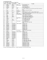
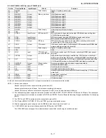
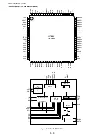
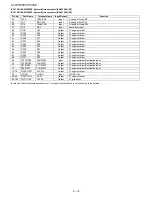
IC1 VHiLC78648E-1: CD Digital Signal Processor (LC78648E) (2/2)
In this unit, the terminal with asterisk mark (*) is (open) terminal which is not connected to the outside.
The same potential must be supplied to all power supply pins, i, e., AVDD1, AVDD2, XVDD, DVDD, LVDD and RVDD)
Pin No.
Terminal Name
Input/Output
Setting in Reset
Function
44
RCHO
Output
RVDD /2
Right channel
D/A converter
R channel Power supply pin.
45
RVDD
—
—
R channel output supply pin.
46
XVSS
—
—
Digital GND pin. Must always be connected to 0V
47
XOUT
Output
Oscillator
Crystal
oscillator
Power supply for crystal oscillator.
Connected for a 16.9344 MHz crystal oscillator pin.
48
XIN
Input
Oscillator
49
XVDD
—
—
Digital power supply pin. Must always be connected to 0V
50
IOMODE
Input
—
CONT4 to 6.MONI3~5, DRF, WRQB pin output mode switching input pin.
”L” setting: Normal output “H” setting: Nch open drain output
51
F16MIN
Input
—
DF. DAC external clock input pin.
52*
OUT1
Output
L
General-purpose output pin 1.
53
16MOUT
Output
CLK
Output
16.9344 MHz output port.
54
ASLRCK
Input
—
Anti-shock
Left/Right clock input pin.
(Must be connect to 0 V when unused.)
55
ASDACK
Input
—
Bit clock input pin.
(Must be connect to 0 V when unused.)
56
ASDFIN
Input
—
Left/Right channel data input pin.
(Must be connect to 0 V when unused.)
57
LRSK
Output
L
Digital data out-
put
Left/Right channel data output pin.
58
DATACK
Output
L
Bit clock output pin.
59
DATA
Output
L
Left/Right clock output pin.
60
DVDD
—
—
Digital power supply pin.
61
DVSS
—
—
Digital GND pin 2. Must always be connected to 0V.
62
CE
Input
—
Microcomputer
Interface
Chip enable signal input pin.
63
CL
Input
—
Data transfer clock input pin.
64
DI
Input
—
Data output pin.
65
DO
Output
(H)
Data output pin. (Try state output.)
66
WRQB
Output
L
Interruption signal output pin.
67
RESB
Input
—
Reset input pin for LSI.
This pin must be set LOW briefly after power is first applied.
68
DRF
Output
L
Focus ON detection pin.
69
C2F/SBCK
Input/Output
Input
Error flag monitor pin, or sub code
read clock input pin.
Controlled by commands from the micro-
processor.
70
CONT6/SBCK
Input/Output
Input
General-purpose I/O pin 6, or sub
code read clock input pin.
Controlled by commands from the micro-
processor.
Any of these that are unused must be either
set up as input pin ports and connected to
0V, or set up as output pin ports and left
open.
71*
MONI5
Output
L
Internal signal monitor pin 5.
72*
MONI4
Output
L
Internal signal monitor pin 4.
73
MONI3
Output
L
Internal signal monitor pin 3.
74
CONT5
Input/Output
Input
General pur-
pose I/O pin 5.
Controlled by command from the microprocessor. Any of
these that are unused must be either set up as input pin
ports and connected to 0V, or set up as output pin ports and
left open when unused.
75
CONT4
Input/Output
Input
General pur-
pose I/O pin 4.
76
PDO1
Output
—
PLL
Phase comparison output pin 1 to control built-in VCO.
77
PDO2
Output
—
Phase comparison output pin 2 to control built-in VCO.
78
PCKIST
Input
—
Resistor connection pin to set current for PDO1 and 02 out-
puts.
79
VVSS
—
—
Built-in VCO GND pin. Must always be connected to 0V.
80
VVDD
—
—
Built-in VCO power supply pin.
Summary of Contents for Illustration XL-HP535E
Page 15: ...XL HP535H HP535E 3 5 MEMO ...
Page 22: ...XL HP535H HP535E 5 3 MEMO ...
Page 86: ...XL HP535E HP535H 13 M E M O ...
Page 87: ...XL HP535E HP535H 14 M E M O ...

