background image


PCUSFO 

P F L T - 0 4 0 5 A F Z Z

129
130
131
132

 Power Supply

Cord

Nylon 

Belt

 Chassis
 

 Lever

Felt, Leg
Magnet

AC Power Supply Cord

Sheet

 Chassis

Sheet

 1 [Australia


 Volt

 [Australia


Screw, 


Screw, 


Screw,     12mm

ACCESSORIES/PACKING PARTS

QCNW- 

Connecting 

A N

  A C   P l u g   A d a p t o r
  A C   P l u g   A d a p t o r

Packing Add.
Packing Case
Polyethylene 

 Holder

Cushion

 Holder

Polyethylene Bag,

Accessories

A F
A E
A C
A H
A D
A A
A H
A B
A A

Warranty Card [Australia A 

Operation Manual

A R
A D

A C

A K
A A
A D
A B
A C
A E
A B

A A
A C
A B
A A
A E
A C

A L
A L
A H
A B
A A
A A
A A
A A
A A
A A
A A
A A

A A
A B

A B
A B
A B

A A
A A
A A
A A
A A
A A
A A
A A
A A
A A
A A
A A

A A
A A
A A
A A


P.W.B. ASSEMBLY (Not Replacement Item)

PWB-A

Servo PWB

D i s p l a y / S w i t c h   P W B  

(Combined Ass’y)

Power PWB


Writer  and Editor: 

   Reliability Control Center of Audio Systems Group, Sharp Corp.

Summary of Contents for DX-670BK

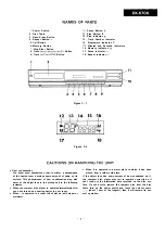
Page 1: ...ION 2 AC POWER SUPPLY CORD AND AC PLUG ADAPTOR 2 NAMES OF PARTS 3 CAUTIONS ON HANDLING THE UNIT 3 DISASSEMBLY 4 5 REPLACEMENT OF PICKUP 5 FITTING OF CD MECHANISM 6 FITTING OF DISC HOLDER 6 BLOCK DIAGRAM 7 FUNCTION TABLE OF IC 8 9 ADJUSTMENT 10 11 EQUIVALENT CIRCUIT BLOCK DIAGRAM OF IC 12 13 TYPES OF TRANSISTOR AND LED 13 NOTES ON SCHEMATIC DIAGRAM 14 SCHEMATIC DIAGRAM WIRING SIDE OF F W BOARD 15 1...

Page 2: ...ut level 2 0 V Recommended impedance 10 kohms Power source AC 110 12712201240 1 50160 Hz Power consumption 10 W Dimensions Width 430 mm 17 Height 80 mm 3 118 Depth 232 mm 9 l 8 Weight 2 8 kg 6 2 Ibs Specifications for this model are subject to change without prior notice VOLTAGE SELECTION The voltage selector is located on the rear of the unit If ad justment is necessary use a screwdriver in order...

Page 3: ...t of dews on its surface This phenomenon of dew condensation may also occur at the object lens in the pickup unit in the following instances l When the compact disc player is operated immediately after you have turned on a heating device in your room l When It is operated in a room full of wet air with steam or moisture l When it is operated in a warm place to which it has been moved from a rather...

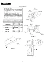
Page 4: ...before disassembling 4 Take sufficient care on static electricity of integrated circuits and circuits when servicing STEP REMOVAL PROCEDURE FIGURE 1 Cabinet 1 Screw Al x 3 4 l 2 Front Panel 1 Screw __ _ 6 x 6 4 2 2 Socket Cl x 3 3 1 Loading Mechanism 1 Screw D x 2 4 3 2 Socket El x 3 4 Servo PWB 1 Screw fF x 3 4 3 2 Socket _ G x 1 5 Disc Holder 1 Push the Rack Gear 4 4 2 Hook H x 2 6 CD Mechanism ...

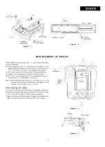
Page 5: ...r and lead wire as it was fdl The laser power adjustment is not necessary owing to improvement of performance of pickup Note When replacing the pickup do not apply force to the turntable of spin motor Otherwise the height of main chassis and turntable may be varied After replacing the pickup This new mechanism has been newly designed to enhance remarkably its performance as compared to the former ...

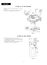
Page 6: ...ading chassis using screws Figure 6 l FITTING OF DISC HOLDER 1 Turn the rack gear in the arrow direction A This causes the disc lever to move to the direction 6 2 While keeping the rack gear in the direction A force fit the disc holder to the chassis 3 Turning the rack gear in the arrow direction C lowers the disk holder so that the disc holder is fixed Figure 6 2 6 ...

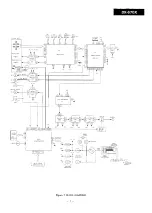
Page 7: ...Figure 7 BLOCK DIAGRAM 7 ...

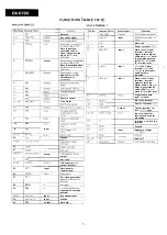
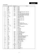
Page 8: ...1 input terminal internal signal to latch the digital audio data CH2 data is generated by using fall of WCLKI when IF is in low level Digital audio data I input terminal I Remote control Tray motor Open tray swnch Ground output Not used Bit clock terminal Power terminal 5 V j Output terminal for test usuallv open I output lnrxt Input terminal for test usually used for grounding interface switching...

Page 9: ...wer terminal Address signal data signal and input control signal Address signal data signal and input control signal Address signal data signal and input control signal Address signal data signal and input control signal Deemphasis control signal Crystal oscillation terminal Synchronizing signal output Not used Synchronizing signal output Not used Synchronizing signal output Not used Not used Grou...

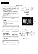
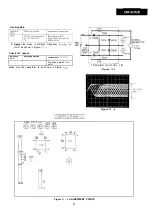
Page 10: ... procedure stated below Focus Offset Adjusting Point Specified value Instrument Connection VR3 0 2 5omv Pin 2 and pin 1 GNDI of CNPZ Tracking Offset Adjusting Point Specified value Instrument Connection VR2 0 Ifr 5 0 mV Pin 4 and pin 1 GND of CNP2 I I Xacking Error Balance Adjusting Point Adjusting method Instrument Connection I I I I VR4 1 Pin 2 and pin 25 GND of IC2 I I I I I Shot t circuit the ...

Page 11: ... 1 l l Check HF output Adjusting Point Adjusting method Instrument ConnectIon Pin 36 and pin 25 GND of IC2 J TRACKING GAIN ADJ JIG Make sure that waveform is as shown in Figure 11 2 Figure 11 1 CNP l l Figure 11 2 1 SERVO PWB A 1 V R 4 V R 3 VRI VR5 VR2 CNP3 Figure 11 3 ADJUSTMENT POINTS 11 ...

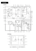
Page 12: ...6 5 Y E SLC Q F 1 2vcc RFS LDD FIVI FIVZ VEE VRl VR2 T 1 17 H F L 516 TES nlYs TES F TE PRI 73 5 1 K IL NJM4560M A OUT A I N A IN VEE Figure 12 EQUIVALENT ClRCUlT BLOCK DIAGRAM OF IC 12 ...

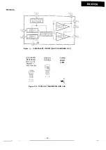
Page 13: ...LENT CIRCUIT BLOCK DIAGRAM OF IC DTAI 14 ES DTC114 ES DTC114YS 2SA562 Y 2SC1740 SR r l FRONT VIEW ii n f E CB l l21 3 2SB1223 2SD1825 LT3P8D FRONT VIEW FRONT VIEW w a B C E Figure 13 2 TYPES OF TRANSISTOR AND LED 13 _ _ __ _ _ _ ...

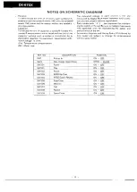
Page 14: ...ofarad As to electrolytic capacitor the expressron capacrtance wrth stand voltage IS used CH Temperature compensation ML Mylar type The lndlcated voltage in each SeCtiOn IS the one measured by Dlgltal Multimeter between such a sec tion and the chassis with no Signal giVen Parts marked with A are important for maintarn ing the safety of the set Be sure to replace these parts with specified ones for...

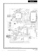
Page 15: ...1 I 2 3 I 4 I 5 I 6 I III 1 I I i I I NOTES ON SCHEMATIC DIAGRAM can be found on page 14 1 1 2 I 3 I 4 I 5 I 6 I 15 figure 15 SCHEM _I ...

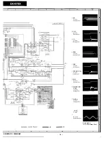
Page 16: ... PDO 2ViDiv 0 5pseciDiv 0 FRF CH D 5VlDiv cli 0 5 sec Div kj FOCUS COIL 1 VlDiv O Ssec Div i i 2 FRF E I 5VlDiv 0 5 sec Div I I fj TRACKING COIL lV Div 0 5seclDiv 7 DATA 2ViDiv O aec Div L O UT R o uT 8 2 VlDiv 0 2m sec Div PLAYBACK 1 kHz Sine Wave Disc H I 7 1 8 I 9 I 10 I 11 I 12 I SCHEMATIC DIAGRAM 16 ...

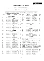
Page 17: ...bber lOmmXl0mmXt8mm Spacer lOmmXlOmmXtO 5mm Sheet Loading Chassis Sheet Holder Fuse Lug Label Class 1 Australia Only1 Label Warning Label Rated Lrne Volt Label Laser Australia Only1 Screw d4X8mm Screw d3XlOmm Screw d3X8mm Screw Q3X8mm Black Screw d3XlOmm Screw d26X5mm Screw r 3X8mm Screw d3X6mm Black Screw d3XlOmm Black Screw 4X6mm Black Screw d4X lOmm Black Screw d3X6mm Screw d 3 X 8mm Screw 43 X...

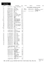
Page 18: ...VRD MN2BD124J R92 VRD MN2BD154J R93 VRD MNZBD224J R94 VRD MN2BD272J R95 VRD MN2BD184J R96 VRD MN2BD154 J R97 VRD MN2BD273J R98 VRD MNZBD8 22 J R99 VRD MN2BD103J RlOO VRD MN2BD823J RlOl VRD MN2BD184J R102 103 VRD MN2BD2R2 J R105 106 VRD MN2BD333J R107 VRD MN2BD473J R108 VRD MN2BD221J RI09 VRD MN2BD124J RllO VRD MN2BD332J R112 VRD MN2BD473J RI13 VRD MNPBD124 J R114 115 VRD MNPBDlROJ RI16 VRD MN2BD22...

Page 19: ...A A A A A A A B A A A A A B A B A B A A A A A A A A A A A B A B A A A A A B A A A A A A A A A B A A A A A B A B A B A B A A A B A B A A A A A B A A A B A B A A A B A A A A A A A A A B A A Unless otherwrse specifvad resrstors are iS carbon type Tubular type carbon film resistor i5 IS rdenbfred the symbol TV TQ CY of the part NO VRS TV TQ CY OOOOOOO this TV TQ CY does not mean lead wrre Tubular type...

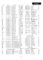
Page 20: ...PN 2SC1740 SR A X AN A N A P A E A H A H A G A E A E A D A E A T AB A C A B AB A B A B A B A B A C A E A F A B A B A B AB A B A B A B A A A B REF NO DlO DZO 23 D301 303 LED1 LED301 ZDlO ll 20301 IT201 Ll dL201 VRl VR2 VR3 4 VR5 Xl x301 PART NO DESCRIPTION VHCSVC203 3F Varrable Capacitance SVC203 VHDllESlTB3 1 Silrcon llESlTB3 VHDlSS133 1 Silicon lSS133 VHPLTSP8D 1 LED Red LT3P8D VHPLT9323H 1 LED O...

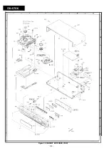
Page 21: ...I38 AUSTRALlA ONLY 119x2 _ CD MECHANISM1 _ I I 5 60 X2 IpwB B21 _ A i I w I a I 0 Figure 20 CABINET EXPLODED VIEW 20 ...

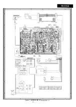
Page 22: ...A e C 0 E F G H L 1 I 2 I 3 I 4 I 5 I 6 1 I 2 I 3 I 4 I 5 I 6 Figure 17 WIRING SIDE OF l W BOARD l 2 17 A B C D E F G H ...

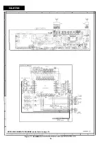
Page 23: ...A e C D E F G H 1 I 2 I 3 I 4 1 5 I 6 DISPLAY PWB Bl NOTES ON SCHEMATIC DIAGRAM can be found on page 14 1 I 2 I 3 I 4 I 5 6 Figure 18 SCHEMATIC DIAGRAM WIRING SlDE OF l W BOARD 2 2 18 ...

Page 24: ...M2 504x2 k I 503x 2 I I I Figure 19 aMf 3 iANISlVl EXPLObED VIEW 3 I 0 19 ...

Reviews: