61
DV-NC55U/C/M
Name
Type
Description
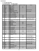
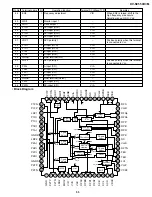
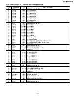
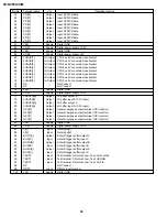
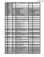
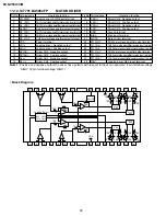
Host interface, CD-DSP interface, sub-code interface (32-pin)...continued
Host ready output (active High). Use this signal when the stream is transferred via
the host bus. External pull-up resistor is required. Prior to transfer of each packet (1
HRDY
O(p.d.)
packet: length in CodBurstLen bytes), make sure that this signal is in the active state,
and then bit streams of CodBurstLen byte long or shorter can be written on this device
consecutively.
Interrupt request (active Low). This is deasserted when the host reads the interrupt
status register of this device and also when the host masks or resets the interrupt
HIRQ#
O(p.u.)
using the interrupt mask register.
When HIRQ# is not asserted, it enters the 3-state mode. (External pull-up resistor is
required.)
Host acknowledge output (active Low). When the protocol is A type, the device asserts
this output and notifies the completion of read or write cycle.
HACK#
O(p.u.)
When this signal is not active, it enters the 3-state mode. (External pull-up resistor is
required.) When the protocol is B type, this signal functions as a wait output signal. If
the high-speed host (microcomputer) is used, this signal may not have to be connected.
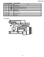
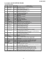
GPI/O signal (3-pin)
GPIO
I/O(r.t.)
General-purpose bidirectional pin monitored and controlled by the ADP micro code.
After resetting, this pin is defined as an input. It can be set by using the ADP command.
GPSI
I
General-purpose input monitored by the DVP micro code.
GPSO
O(p.d.)
General-purpose output controlled by the DVP micro code. After resetting, output
from this pin is switched to Low.
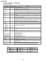
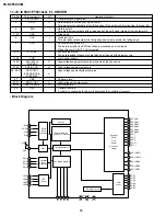
PLL signal (5-pin)
GCLK
ID
27,000 MHz clock or crystal input for main processor.
GCLK1
ID
27,000 MHz master clock input for audio. Normally, this must be connected to GCLK.
XO
AO
Output to crystal connected to GCLK. If the crystal is not used for GCLK, nothing
must be connected to XO.
PLLCFG[1:0]
ID
PLL configuration input. It can be changed only during resetting. Normally, both pins
must be connected to GNDP.
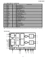
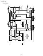
Analog video port (7-pin)
CVBS/G/Y
For CVBS, the composite video signal is output.
(DAC A)
AO
For RGB, the G signal is output.
For YUV, the Y signal is output.
Y/R/V
For CVBS, the Y signal is output.
(DAC B)
AO
For RGB, the R signal is output.
For YUV, the V signal is output.
C/B/U
For CVBS, the C signal is output.
(DAC C)
AO
For RGB, the B signal is output.
For YUV, the U signal is output.
CVBS/C
AO
The CVBS or C signal is selected and output.
(DAC D)
RSET
AI
Resistance load for DAC gain adjustment is inserted between GND and DAC.
VREF
AI
Reference voltage for DAC gain adjustment is input.
COSYNC
O(p.d.)
Composite sync output. Effective only when the RGB analog output is selected.
Otherwise, it is fixed to Low.
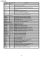
Digital video port (5-pin)
VCLKx2
I/O(r.t.)
Main video clock input or output. 27,000 MHz.
VCLK
I/O(r.t.)
Divided VCLKx2 signal. Used as a qualifier of data and sync signal.
HSYNC
I/O(r.t.)
Horizontal sync bidirectional signal pin. Its polarity and length are programmable.
VSYNC
I/O(r.t.)
Vertical sync bidirectional signal pin. Its polarity and length are programmable.
FI
I/O(r.t.)
Field identification bidirectional signal pin. Its polarity is programmable.

