8
8-1
8-2
CX51TXZ
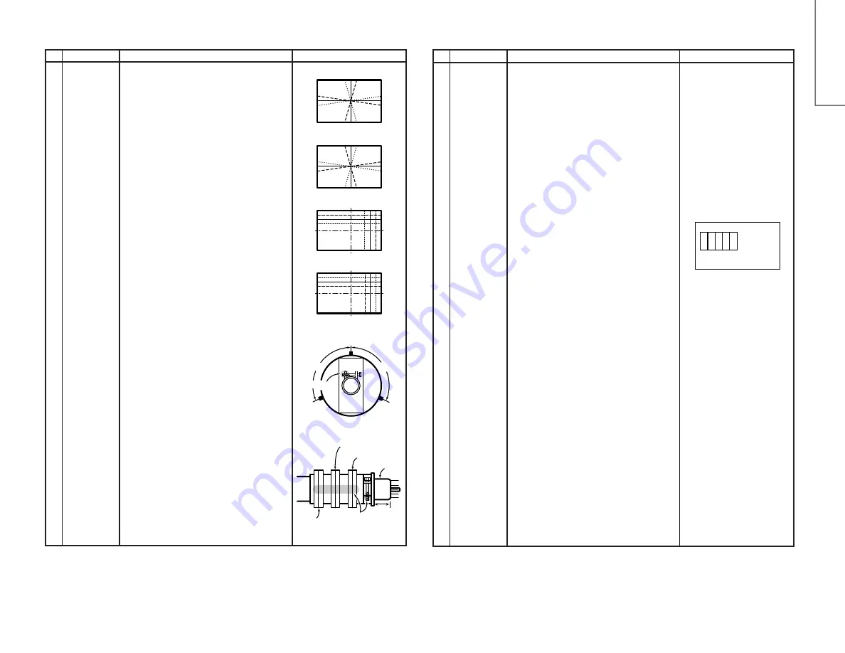
CONVERGENCE ADJUSTMENT
No. Adjusting point
Adjusting procedure/conditions
Waveform and others
Convergence
adjustment
(to be done
after the purity
adjustment)
1. Receive the “Crosshatch Pattern” signal.
2. Using the remote controller, call NORMAL mode.
STATIC CONVERGENCE
1. Turn the 4-pole magnet to a proper opening an-
gle in order to superpose the blue and red col-
ours.
2. Turn the 6-pole magnet to a proper opening an-
gle in order to superpose the green colour over
the blue and red colours.
DYNAMIC CONVERGENCE
1. Adjust the convergence on the fringes of the
screen in the following steps.
a)
Fig. 3-1: Drive the wedge at point “a” and
swing the deflection coil upward.
b)
Fig. 3-2: Drive the wedge at points “b” and
“c” and swing the deflection coil downward.
c)
Fig. 3-3: Drive the “c” wedge deeper and
swing the deflection coil rightward.
d) Fig. 3-4: Drive the “b” wedge deeper and
swing the deflection coil leftward.
2. Fix all the wedges on the CRT and apply glass
tape over them.
3. Apply lacquer to the deflection yoke lock screw,
magnet unit (purity, 4-pole, 6-pole magnets) and
magnet unit lock screw.
Finally received the Red-only and Blue-only sig-
nals to make sure there is no other colours on the
screen.
1
RGB
BGR
R
G
B
R
G
B
B
G
R
B
G
R
RGB
BGR
Fig. 3-2
Fig. 3-1
Fig. 3-3
Fig. 3-4
Fig. 3-5
Fig. 3-6
Lacquer
Wedge "a"
Wedge
"b"
Wedge
"c"
About
100
°
About
100
°
4-pole magnet
6-pole magnet
CRT neck
20mm
Lacquer
Purity magnet
CRT CUT-OFF, BACKGROUND AND SUB-CONTRAST ADJUSTMENT
No. Adjusting point
Adjusting procedure/conditions
Waveform and others
CRT cut-off
adjustment
I
2
C bus
Control
adjustment
1. Receive the the “Monoscope Pattern” signal.
2. Press R/C to set Picture in Normal condition.
3. Call the Service mode and select the “Cut-off/
Background” mode.
4. Set the screen control to 0 / 10 position.
5. Press “-/--” key on the remote controller to reach
the horizontal centering mode.
6. Here one of the three colour will appear as a bright
line when the screen controlis turned clockwise.
Adjust the screen VR until the line can be seen
slightly on the screen.
7. Use the control key in the R/C to adjust the quan-
tity of the other two colours, thus touching off the
bias control belonging to the first colour, until the
horizontal raster becomes white.
8. Turn off the screen control (counter-clockwise)
until the horizontal raster disappears.
Note: Before starting this adjustment , warm
up the unit for 30 minutes or longer at
a beam current of over 700 µA.
9. Press the “-/--” key on the remote control to call
the NORMAL mode.
10.Call “SUB-BRIGHT” in SERVICE mode. (Receive
Crosshatch Signal with 5 black level window)
11.Adjust the “SUB BRIGHT” bus data in order that
the line 1, 2 and 3 have the same darkness
wherelse line 4 is slightly brighter than line 1, 2
and 3 and finally line 5 will be the brighter than
line 4.
12.The range of the “SUB BRIGHT” must be between
107 and 157(127 +30, –20). (If the “SUB BRIGHT”
is out of the range as mention above, please do
adjust from step 1. to 11. again.)
Note: Steps 10. and 11. should be adjusted af-
ter WHITE BALANCE ADJUSTMENT.
For the “SUB BRIGHT” out of range
mention above, it will result in the dif-
ferent brightness of OSD.
1
* Before adjustment , make sure
that this adjustment with the ini-
tial bus data
“R-CUT OFF”, “G-CUT OFF”,
“B-CUT OFF”, “B-DRIVE” &
“G-DRIVE”.
Note:
R CUT OFF UP
“1” KEY
DOWN “4” KEY
G CUT OFF UP
“2” KEY
DOWN “5” KEY
B CUT OFF UP
“3” KEY
DOWN “6” KEY
The data can be turned up
and down with the above
keys.
Make sure all the 1st, 2nd and
3rd black portions are at the
same black level.
1 2 3 4 5
Summary of Contents for CX51TXZ
Page 24: ...24 CX51TXZ CHASSIS LAYOUT 6 5 4 3 2 1 A B C D E F G H ...
Page 28: ...28 8 7 10 9 6 5 4 3 2 1 A B C D E F G H CX51TXZ SCHEMATIC DIAGRAM MAIN Unit ...
Page 29: ...29 17 16 19 18 15 14 13 12 11 10 CX51TXZ ...
Page 32: ...32 8 7 10 9 6 5 4 3 2 1 A B C D E F G H CX51TXZ BLOCK DIAGRAM 1 3 Ys Ym ...
Page 33: ...33 17 16 19 18 15 14 13 12 11 10 CX51TXZ ...
Page 34: ...34 8 7 10 9 6 5 4 3 2 1 A B C D E F G H CX51TXZ 6 5 4 3 2 1 A B C D E F G H BLOCK DIAGRAM 2 3 ...
Page 35: ...35 17 16 19 18 15 14 13 12 11 10 CX51TXZ 6 5 4 3 2 1 A B C D E F G H BLOCK DIAGRAM 3 3 ...
Page 37: ...37 17 16 19 18 15 14 13 12 11 10 CX51TXZ ...
Page 38: ...38 8 7 10 9 6 5 4 3 2 1 A B C D E F G H CX51TXZ PWB A MAIN Unit Chip Parts Side ...


