CD-C471
Note:
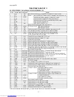
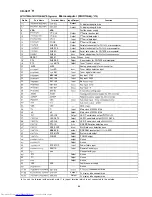
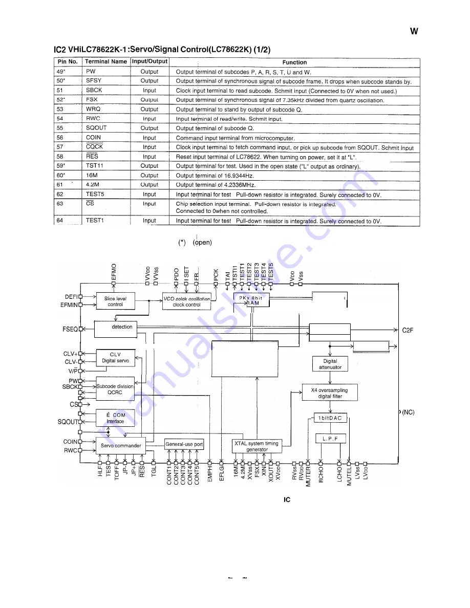
The same potential must be supplied to the, power terminals (VDD, VVDD, LVDD, RVDD, XVDD).
In this unit, the terminal with asterisk mark
is
terminal which is not connected to the outside.
g
e
n
e
r
a
t
o
r
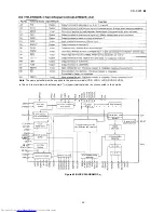
RAM address
Sync
EFM demodulation
Interpolation mute
Bilingual
I
I
I
Digital OUT
DOUT
Flag processing of Cl/C2
error detection and correction
SBSY
SFSY
WRQ
CQCK
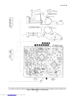
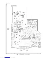
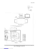
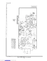
Figure 45 BLOCK DIAGRAM OF
45
Summary of Contents for CD-C471 W
Page 16: ... I I Ill I i c r __ __ I Figure 16 BLOCK DIAGRAM 2 3 16 ...
Page 17: ...CD C471 W w UTER lC56115621563 N5M4558L lC562 1 2 Figure 17 BLOCK DIAGRAM 3 3 17 ...
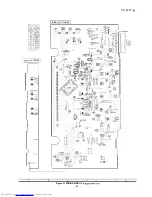
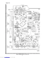
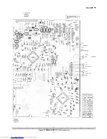
Page 36: ... POWER PWB B 1 MAII IUPWB P33 7 A 1 2 3 4 5 6 Figure 36 WIRING SIDE OF P W BOARD 6 8 36 ...
Page 54: ...CD C471 W MEMO 54 ...
Page 70: ......
Page 71: ...CD C471 W MEMO ...

