background image

CD-BP1450V

– 8 –

1

Top Cabinet

1. Screw ..................... (A1) x4

8-1

2

Side Panel

1. Screw ..................... (B1) x2

8-1

(Left/right)

2. Screw ..................... (B2) x2

3

CD Player Unit/

1. Turn on the power supply,

8-2

CD Tray Cover

    open the disc tray, take out the
    CD cover, and close.   (Note 1)
2. Screw ..................... (C1) x1
3. Hook ....................... (C2) x3
4. Hook ....................... (C3) x2
5. Socket .................... (C4) x3

4

Rear Panel

1. Screw ..................... (D1) x8

8-2

5

Main/Headphones 1. Screw ........................ (E1) x8

9-2

PWB

2. Socket .................... (E2) x4
3. Flat Cable .............. (E3) x1
4. Lug Wire ................. (E4) x1

6

Front Panel

1. Screw ..................... (F1) x3

9-2

7

Display PWB

1. Screw ..................... (G1) x9

9-3

2. Flat Cable .............. (G2) x1

8

Tape Mechanism 1. Open the cassette holder.

9-3

2. Screw...................... (H1) x5

9

Turntable

1. Hook ....................... (J1) x2

9-4

2. Cover ..................... (J2) x1

10

Disc Tray

1. Turn fully the lock  lever in the

8-3

    arrow direction.
2. While holding the lock lever, rotate

9-1

    the cam gear until the cam gear
    rib engages with the clamp lever.
3. Push the slide holder backward to

9-5

    engage the claw with the groove
    and remove it in the direction
    of the arrow. .............. (K1) x6

11

CD Servo PWB

1. Screw ..................... (L1) x1

9-6

(Note 2)

2. Hook ....................... (L2) x3
3. Socket .................... (L3) x4

12

CD Mechanism

1. Hook ....................... (M1) x2

10-1

2. Hook ....................... (M2) x3

13

Loading Motor PWB 1. Hook ....................... (N1) x5

10-1

DISASSEMBLY

Caution on Disassembly
Follow the below-mentioned notes when disassembling
the unit and reassembling it, to keep it safe and ensure
excellent performance:
1. Take cassette tape and compact disc out of the unit.
2. Be sure to remove the power supply plug from the wall

outlet before starting to disassemble the unit.

3. Take off nylon bands or wire holders where they need to

be removed when disassembling the unit. After servicing
the unit, be sure to rearrange the leads where they were
before disassembling.

4. Take sufficient care on static electricity of integrated

circuits and other circuits when servicing.

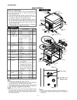
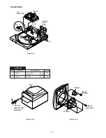
Figure 8-2

Figure 8-3

STEP

REMOVAL

PROCEDURE

FIGURE

Note 1:
How to open the changer manually. (Fig. 8-3)
1.  In this state, turn fully the lock lever in the arrow direction

through the hole on the loading chassis bottom.

2. While holding the lock lever, rotate the cam gear anti clockwise

until the cam gear rib engages with the clamp lever. (Fig. 9-1)

3.  After that, push forward the CD slide holder.
Note 2:
1. After removing the connector for the optical pickup from the

connector, wrap the conductive aluminium foil around the
front end of the connector to protect the optical pickup from
electrostatic damage.

Figure 8-1

Note 3:
1. Be careful not to break the claw of the CD mechanism.
2. When fining back the cam gear assembly, let it lock by front

movement.

(B2)x1
ø3x10mm

(B2)x1
ø3x10mm

Side Panel
(Right)

Side Panel
(Left)

Top Cabinet

Rear
Panel

(A1)x2
ø3x12mm

(A1)x2
ø3x12mm

(B1)x2
ø3x12mm

Front Panel

(C3)x1

(C1)x1
ø3x12mm

(D1)x8
ø3x8mm

CD Player
Unit

CD Tray  Cover

Rear
Panel

Pull

(C3) x1

(C2) x3

1

1

2

Main PWB

Front Panel

(C4)x3

Video CD PWB

Lock Lever

CD Player Unit
(Bottom View)

CD-BP1450V

CD-BP1450V

Summary of Contents for CD-BP1450V

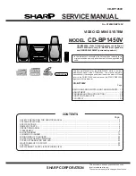
Page 1: ...AL This document has been published to be used for after sales service only The contents are subject to change without notice CD BP1450V Video CD Mini System consisting of CD BP1450V mainunit CP BK1450 front speakers and GBOXS0043AWM1 surround speakers SHARP CORPORATION MODEL CD BP1450V VIDEO CD MINI SYSTEM NTSC PAL This Service Manual is for the CD BP1450V which is a minor modification model of t...

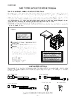
Page 2: ...ntil the appropriate voltage number appears in the window 110 V 127 V 220 V or 230 V 240 V AC QACCE0007AW00 Figure 2 AC POWER SUPPLY CORD AND PLUG ADAPTOR QPLGA0003AWZZ QPLGA0004AWZZ QACCA0004AW00 CAUTION This Video CD Mini System is classified as a CLASS 1 LASER product The CLASS 1 LASER PRODUCT label is located on the rear cover Use of controls adjustments or performance of proce dures other tha...

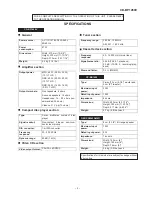
Page 3: ... 20 20 000 Hz Dynamic range 90 dB 1 kHz Video output format PAL PAL 60 NTSC Frequency range FM 88 108 MHz AM 531 1 602 kHz Frequency response 50 14 000 Hz Normal tape Signal noise ratio 55 dB TAPE 1 playback 50 dB TAPE 2 recording play back Wow and flutter 0 3 WRMS Type 2 way 13 cm 5 1 4 woofer and 5 cm 2 tweeter Maximum input power 30 W Rated input power 15 W Impedance 8 ohms Dimensions Width 220...

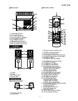
Page 4: ...own Buttons 21 Tuning and Time Up Down Buttons 22 TAPE 1 Cassette Compartment 23 TAPE 2 Cassette Compartment 24 VCD CD Disc Skip Button 25 VCD CD Audio Mode Button 26 VCD Playback Control Button 27 VCD On Screen Display On Off Button 28 VCD Digest Button 29 VCD Bookmark Button 30 VCD CD Open Close Button 31 Memory Set Button 32 VCD Skip Previous Button CD Track Down Review Button TUNER Preset Down...

Page 5: ...rch Button 8 VCD Digest Time Search Button 9 VCD CD Clear Button 10 VCD CD Memory Button 11 VCD CD Disc Skip Button 12 VCD Skip Previous Button CD Track Down Review Button TUNER Preset Down Button TAPE 2 Rewind Button 13 VCD Bookmark Button 14 VCD PAL NTSC Select Button 15 TAPE 2 Record Pause Button 16 Function Selector Buttons 17 VCD CD Random Button 18 VCD CD Pause Button 19 VCD Skip Next Button...

Page 6: ...s where the AC wall socket and AC power plug can be directly connected see illustra tion Note for users in Australia and New Zealand An AC plug adaptor is not supplied if the lead has an Austra lian Standard plug AM FM interval span The International Telecommunication Union ITU has established that member countries should maintain either a 10 kHz or a 9 kHz interval between broadcasting frequen ci...

Page 7: ...ow to change the clock time To change the clock time 1 Press the CLOCK button 2 Within 5 seconds press the MEMORY SET button 3 Perform steps 6 9 above To change the time display mode 1 Perform steps 1 2 in RESETTING THE MICROCOM PUTER 2 Perform steps 1 9 above Main unit operation 0 00 The 24 hour display will appear 0 00 23 59 AM 0 00 The 12 hour display will appear AM 0 00 PM 11 59 AM 12 00 The 1...

Page 8: ...e sure to remove the power supply plug from the wall outlet before starting to disassemble the unit 3 Take off nylon bands or wire holders where they need to be removed when disassembling the unit After servicing the unit be sure to rearrange the leads where they were before disassembling 4 Take sufficient care on static electricity of integrated circuits and other circuits when servicing Figure 8...

Page 9: ... Chassis Loading Chassis L3 x2 L2 x3 L3 x2 CD Servo PWB Slide Chassis L1 x1 ø3x8mm E2 x2 E2 x1 E2 x1 E3 x1 Headphones PWB E1 x7 ø3x10mm Main PWB E1 x1 ø3x10mm E4 x1 F1 x3 ø3x8mm Front Panel G1 x10 ø3x10mm G2 x1 H1 x5 ø3x10mm Display PWB Open Cassette Cover Tape Mechanism Front Panel Clamp Lever CD Player Unit Top View Cam Gear Rib Figure 9 1 ...

Page 10: ...iver should be pried away from speaker box A1x1 Tweeter B1 x2 ø3x10mm A2 x4 ø4x12mm Woofer 1 Woofer 1 Front Panel A1 x1 10 2 2 Screw A2 x4 2 Tweeter 1 Screw B1 x2 10 3 STEP REMOVAL PROCEDURE FIGURE Figure 10 1 M2 x3 M1 x1 N1 x5 M1 x1 Loading Motor PWB CD Mechanism ...

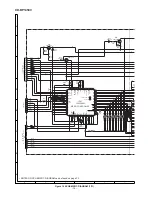
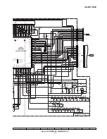
Page 11: ...5 76 45 53 46 47 48 32 31 30 40 65 66 67 68 69 70 71 72 CE CL DI DO INT WRQ RES DEF 52 51 XOUT XIN 73 5 18 36 44 49 50 7 3 14 15 16 19 23 24 25 26 33 59 57 35 54 55 56 17 18 19 20 21 22 30 23 11 9 1 4 5 6 7 15 16 26 27 2 17 25 41 42 38 39 35 29 22 21 14 8 40 18 24 23 28 SW4 PICKUP IN 3 3V QV3 B5 XV1 4 19MHz 7 XV2 27MHz ICV1 MPEG CONTROLLER IX0352AW ICV2 D61012GC MPEG DECODER ICV3 SDM4260C DRAM MBU...

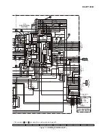
Page 12: ...ITCHING Q104 Q107 L T2 R T2 R T1 L T1 IC101 AN7345K PLAYBACK AND RECORD PLAYBACK AMP R L FM AM MPX IN STEREO AM RF IN AM OSC IN FM B Q360 VT FM OSC 4 5MHz X352 COVERAGE AM BAND AM TRACKING T303 Q302 X351 MO ST VCO DET FM FM B GND AM IF CF351 IC303 LA1832S FM IFDET FM MPX AM IF AM MIX CF352 T351 RF FM OSC FM L312 CF303 T302 FM FRONT END TA7358AP IC301 BF301 FM ANTENNA TERMINAL 22 3 21 4 24 2 1 8 18...

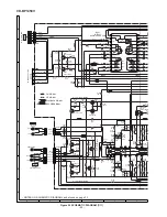
Page 13: ...50V F802 T3 15A L 250V Vcc Vcc POWER AMP STK402020 IC901 BAIS AVDD KEY SW701 SW721 SW723 SW725 SECTION TO CD AC POWER SUPPLY CORD AC 110 127 220 230 240V 50 60Hz T F IC701 IX0338AW SYSTEM MICROCOMPUTER FL DISPLAY FL701 10 13 8 9 1 15 7 1 3 33 32 31 71 30 11 10 6 5 4 1 2 99 80 33 31 45 7 111213 9 10 15 16 17 20 21 23 22 24 100 78 60 5957 565554 5352 50 51 49484746 44 43424140 39 38 37 36 35 34 4 2 ...

Page 14: ...F 7 6 5 4 1 2 3 KEY CONT VOCAL CANCEL HD0 HD1 K_C_STRB K_C_CLK K_C_DATA VSS0 VDD0 PWR_MPEG MDI MDO MCK SBUSY MBUSY VDD1 AVSS HD7 HD6 HD5 HD4 HD3 HD2 AVREF AVDD RESET XT2 XT1 IC X2 X1 VSS1 INT HCS HRD HWR HDAK HA MPEG RESET CD LD M CD LD M CD SOL MO_SPEED 2 3 1 10 8 18 4 3 2 16 11 12 14 13 15 19 17 6 1 7 5 9 ICV1 IX0352AW MPEG CONTROLLER QV2 KTA1298 Y CV1 47 6 3 RV1 10K RV2 1K DV4 KDS193 QV3 KRC104...

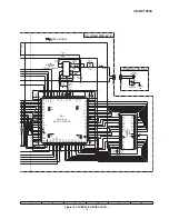
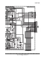
Page 15: ...RAS MA0 MA1 MA2 MA3 VDD MA4 MA5 MA6 MA7 MA8 VDD AUDO AUEMPH AULRCK AUBCK AUCLK INT HDAK RESET VDD HSELA HSELX HA HWR HRD HCS VDD CKSEL VDD X2 X1 HD0 HD1 HD2 HD3 GND GND GND GND GND GND GND GND GND GND GND GND GND GND HD4 HD5 HD6 HD7 GND VDD VSS DQ15 DQ14 DQ13 DQ12 VSS DQ11 DQ10 DQ9 DQ8 LCAS UCAS OE A8 A7 A6 A5 A4 VSS VDD A3 A2 A1 A0 RAS WE DQ7 DQ6 DQ5 DQ4 VDD DQ3 DQ2 DQ1 DQ0 VDD VIDEO SIGNAL CD VI...

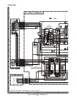
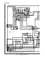
Page 16: ...38 39 40 41 42 8 7 6 5 4 3 2 1 NC NC SLDO FDO TDO LOADING M VCC3 VCC2 SPN VCC4 LD_M LD_M LOADING M SP SP SPO MUTE Vref STANDBY VCC1 SL SL GND GND TR TR FO FO FO FD TO 8 7 6 5 4 3 2 1 GND D PUIN SP SP SL SL 6 2 3 1 4 5 6 2 3 1 4 5 6 2 3 1 4 5 6 2 3 1 4 5 M M TDO SPDO EFBL FIN2 FIN1 TIN2 TIN1 CD VIDEO PWB B 2 2 8 LASER DRIVER C8 0 022 C7 10 16 C20 0 1 C14 0 33 R56 68K R55 68K R54 68K R53 68K R52 68K...

Page 17: ...IT DAC LPF INTERPOLATION MUTE ATTENUATION DEEMPHASIS AUDIO OUT ERROR CORRECT FRAME SYNC DEFECT PROTECT EFM DECODE CLV CONTROL CLOCK GENERATOR GENERAL SUBCODE DECODE CRC COMMAND INTERFACE GENERAL SW SERVO PROCESSEROR AUTO ADJUST S H JITER DEFECT CONTROL A D SW SLICE LEVEL CONTROL PLL VCEC D A CONT7 CONT6 CE CL DI DO WRQ RES DEF VSS V vP FSEQ DEFECT 3 2 1 NG M PN NG M TDO SLDO FDO RES WRQ CE CL DI D...

Page 18: ... 21 27 28 29 26 30 2 3 4 5 1 7 8 9 6 12 13 14 15 11 17 18 19 10 16 22 23 24 25 21 27 28 29 20 26 30 31 52 53 54 55 51 52 53 54 51 57 58 59 56 60 62 63 64 65 61 67 68 69 66 70 72 73 74 75 71 77 78 79 76 80 80 32 33 34 35 31 37 38 39 36 40 42 43 44 45 41 47 48 49 46 50 B B B B B B B B B 13 12 11 10 9 8 7 2 1 3 4 5 6 M TAPE MECHANISM PWB D TAPE MOTOR SOLENOID SOLENOID FFC13 PH PH T2 PALAY R PALAY T1 ...

Page 19: ... 21 1 CNP701 TO MAIN PWB P21 12 D CNS702 FFC21 P17 12 E R778 1K R726 2 2K R727 2 2K R728 2 2K R729 2 2K R719 1K R720 1K R721 1K R722 10K R724 1K R717 1K R716 1K R715 1K R714 1K R713 1K R712 1K R711 1K R710 1K R709 1K R706 1K R703 1K R702 1K R707 1K R704 1K R708 1K R705 1K C704 18P C703 15P XL701 C702 220 10 C701 0 022 R745 100K C707 1 50 Q701 KRC107 M R744 1K R725 1K R755 4 7K L701 100µH R770 47K ...

Page 20: ...601 330 C603 22 25 R625 22K BI601 CNS601 IC601 LC75341 AUDIO PROCESOR C633 0 0033 C623 1 50 C625 1 50 C627 1 50 C629 1 50 R615 3 9K R617 3 3K C607 10 50 C617 1 50 C609 0 1 ML C611 0 1 ML C613 0 0027 C628 1 50 C626 1 50 C624 1 50 C630 1 50 C610 0 1 M C612 0 1 M C618 1 50 C614 0 00 C608 10 50 C606 22 50 R101 10K C101 0 047 R157 100 R104 1K R102 10K Q102 KRC104 M R137 10K Q103 KRC104 M R103 4 7K C108...

Page 21: ...A1 1 3 26 27 28 25 31 32 33 30 29 CNS701 34 36 37 38 35 41 42 43 40 39 IC101 PLAYBACK AND RECORD PLAYBACK AMP 1 2 3 50 9kHz 100 10kHz MUTING MUTING SWITCHING BIAS BIAS OSC 1 21 C604 100 16 C628 1 50 C626 1 50 C624 1 50 C630 1 50 C610 0 1 ML C612 0 1 ML C618 1 50 C614 0 0027 C608 10 50 C606 22 50 C634 0 0033 R618 3 3K C605 0 022 R616 3 9K C139 3 3 50 C127 270P C135 47 25 C129 22 25 R127 6 8K R129 2...

Page 22: ...8 100 Fusible R954 0 1 1W R93 21K R936 1K C934 3P C936 10 50 R934 56K R948 1K C949 0 001 C932 220P C942 10 50 R942 39K R933 56K R943 47K R945 10K Q902 KTA1268 GR C935 10 50 R941 39K C941 10 50 R944 1K R940 10K Q903 KTC3200 GR C815 2200 50 R811 22K R812 22K Q904 KTC3199 GR Q901 KTC3199 GR R953 1K C943 100 16 R952 33K R951 47K Q805 KTD2026 C814 2200 50 R814 33 C826 22 25 R815 22K C827 0 047 ML IC801...

Page 23: ...00µH L902 0 29µH L901 0 29µH R907 330 C919 0 1 ML C920 0 1 ML C918 0 1 ML C917 0 1 ML R910 4 7 1 4 R909 4 7 1 4 C916 22 50 C915 22 50 SO901 SPEAKER TERMINAL D814 D3SBA60F C816 0 047 ML C817 0 047 ML F802 T3 15A L 250V CNP801 F801 T2A L 250V C813 0 047 ML C812 0 047 ML D811 1N4004S D813 1N4004S D810 1N4004S D812 1N4004S R810 12K C810 100 35 ZD802 DZ6 2ASA C809 47 50 C808 47 50 R807 2 2K ZD801 DZ300...

Page 24: ...0 2 7K C367 1 50 C361 0 022 R351 5 6K C353 0 022 CF352 AM IF R352 1K T351 C350 0 022 C352 10 16 C351 0 022 CNP302 BF301 BAND PASS FILTER IC301 TA7358AP FM FRONT END C305 4 7P CH C304 0 01 C306 0 022 C307 10 16 SO302 FM ANTENNA TERMINAL C301 0 001 C309 0 001 D305 DS1SS133 L312 C308 4 7P VD302 KDV147B R313 33K C310 15P CH C311 18P C324 8 2P UJ C313 22P CH T301 C312 0 022 CF303 C387 0 022 C392 0 001 ...

Page 25: ...SOLENOID PH SW SW SW PH SOLENOID TAPE MECHANISM PWB D TAPE MECHANISM ASSEMBLY P28 5 G TO DISPLAY PWB CNP101 P26 1 D TO MAIN PWB P26 1 E TO MAIN PWB CNP102 TAPE 1 PLAYBACK HEAD TAPE 2 ERASE HEAD RECORD PLAYBACK HEAD FFC13 BL WH YL BK PK WH BK BK BK RD WH WH WH PK BK 1 2 3 4 5 6 7 GR GR GR 2 3 1 BL YL WH RD CNP802 P26 2 B TO MAIN PWB YL BK YL BR BR WH WH PT801 POWER TRANSFORMER 1 2 3 4 5 6 7 1 2 3 4...

Page 26: ...611 R948 R362 R364 R361 R363 C355 R3 C601 C C602 R603 R604 R609 R615 C633 R617 R618 R135 C131 R131 C634 R129 R616 C137 R123 C143 R125 C923 R144 R101 R102 R103 C104 R148 R147 R111 R112 C105 C103 R113 R108 R110 R137 C106 C107 R106 R107 R109 C102 R105 C113 C112 C114 C115 R118 R124 R120 R119 R121 C120 C121 R126 C127 R127 R130 R133 C130 C132 R132 C133 C145 R136 R141 R140 C144 C126 R128 R134 2 3 4 5 1 7...

Page 27: ... C381 C386 C392 R377 R385 C318 C385 R393 R380 R383 R322 R325 C324 R327 R302 C311 C310 C313 C312 R353 C315 C399 C308 R311 C366 R351 C314 R365 R313 C317 R316 C316 C369 C334 R350 C361 R336 R356 R323 C363 C342 C332 C335 R362 R364 R361 R363 C355 R355 C601 C356 C602 R603 R604 R609 R615 C633 R617 R618 6 R395 R378 C302 C309 C353 R352 C354 C350 C351 C387 R379 2 3 4 5 1 7 8 9 6 12 11 10 2 3 4 5 1 7 8 9 6 11...

Page 28: ...OLUME UP Q706 Q704 Q705 SW713 VOLUME DOWN SW724 TUNING TIME UP SW716 TUNING TIME DOWN SW F FOR R702 R701 R703 R704 RD07 SW708 BOOK MARK SW70 DIGES RD06 RD17 RD20 RD19 RD26 RD09 R708 R744 C718 R745 RD25 RD10 RD11 R768 R766 R767 RD12 RD23 22 23 24 25 21 27 28 29 26 30 32 33 31 2 3 1 1 2 3 B C E B C E B C E TO TAPE MECHANISM PWB FFC13 13 1 P25 8 A 1 1 3 5 7 9 1113 12 10 8 6 4 2 DISPLAY PWB A2 BR COLO...

Page 29: ...W725 TUNER BAND SW719 FAST FORWARD 80 81 100 1 5 10 15 20 25 30 31 35 40 45 50 51 55 60 65 70 75 85 90 95 R770 C714 RD02 R772 R760 RD04 R763 RD13 RD24 RD15 RD16 R719 R777 R720 R776 R721 R775 R722 R778 R757 R756 R759 R749 R750 R751 R761 R758 R762 R748 R737 R736 R735 R734 R742 IC701 R733 R702 R701 4 C704 C703 D07 SW707 DIGEST SW705 P B C SW704 AUDIO MODE SW706 OSD RD06 RD17 R753 BI702 12 1 101112 1 ...

Page 30: ... R25 R47 IC1 ZD61 R58 Q1 C22 C17 R10 R19 C20 R8 R39 R38 R35 R44 R79 C23 C29 C82 C27 C42 C26 R15 R80 R13 R12 IC2 C80 R20 L61 Q2 CNP2 XL1 1 1 5 10 15 16 20 25 30 5 10 15 20 21 22 25 30 35 40 42 1 5 10 15 20 25 30 32 33 35 40 45 48 49 50 55 60 64 16 17 2 1 121110 9 1 1 1 2 3 4 5 6 7 1 1 2 3 4 5 6 1 2 3 4 5 6 2 3 4 5 6 7 8 2 3 4 1 5 10 15 20 24 25 30 35 40 41 45 50 55 60 64 65 70 75 80 CNS702 FROM DIS...

Page 31: ...39 CV15 CV41 CV40 C51 C18 R7 C11 R74 R71 R78 R72 R76 R77 R11 R14 C41 C47 C50 C49 RV60 CV14 ICV2 CV13 R90 C39 1 1 1 4 5 8 5 10 15 20 40 45 55 60 65 70 75 76 80 85 90 95 100 50 51 35 25 26 30 5 10 11 15 21 25 30 31 35 40 20 1 2 CD VIDEO PWB C TOP VIEW VIDEO OUT PWB A4 M1 SPINDLE MOTOR 1 7 1 8 CNS1B CNS1A CNS2B CNS2A CNS3B CNS3A RD WH GY WH GY WH GY WH RD WH GR WH GR WH 1 2 3 4 5 6 7 8 1 2 3 4 5 6 7 ...

Page 32: ... capacitance withstand voltage is used CH TH RH UJ Temperature compensation ML Mylar type P P Polypropylene type Schematic diagram and Wiring Side of P W Board for this model are subject to change for improvement without prior notice REF NO DESCRIPTION POSITION POSITION REF NO DESCRIPTION SW1 OPEN CLOSE ON OFF SW2 CLAMP ON OFF SW3 DISC NUMBER ON OFF SW4 PICKUP IN ON OFF SW601 SPAN SELECTOR 50 9kHz...

Page 33: ...MAL Type EDGE CH2 Delay 2 924ms Hold off 0 2µs CH3 0 00V CH4 0 00V BW FULL Trigger Filter Offset 1 IC2 24 6 IC2 25 T FDO PDO2 PDO1 Stopped CH1 500mV DC 10 1 CH3 1V DC 10 1 CH4 1V DC 10 1 500ms div 500ms div NORM 20kS s 1 4 3 Record Length Smoothing ON CH1 0 000V CH2 0 0V Main 100K Zoom 2K Mode AUTO Type EDGE CH2 Delay 0 0ns Hold off 0 2µs CH3 0 00V CH4 0 00V BW FULL Trigger Filter Offset CH1 v DIV...

Page 34: ...6V 0V 0V 0V 0V 0V 0V 17 16 15 14 13 20 19 18 1 9V 1 9V 0 5V 0 5V 0V 0V 0V 0V 21 24 23 22 PIN NO VOLTAGE IC101 4 96V 4 96V 0V 0V 0V 4 96V 4 96V 4 89V 4 78V 4 78V 4 78V 4 78V 9 8 7 6 5 4 3 2 1 12 11 10 4 78V 4 78V 4 78V 4 78V 5 1V 5 5V 5 0V 4 66V 17 16 15 14 13 20 19 18 5 03V 4 97V 10 0V 0V 21 24 23 22 PIN NO VOLTAGE IC601 0 1V 9 9V 4 6V 4 7V 2 4V 2 4V 0V 0V 0V 0V 0V 0V 4 8V 4 9V 4 2V 0V 0V 0V 0V 0V...

Page 35: ...ithout lead wire VC TV Square type without lead wire VC TQ Square type without lead wire VC CY Square type without lead wire VC CZ Square type without lead wire VC J The 13th character represents capacity difference J 5 K 10 M 20 N 30 C 0 25 pF D 0 5 pF Z 80 20 If there are no indications for the electrolytic capacitors error is 20 Resistors VRD Carbon film type VRS Carbon film type VRN Metal film...

Page 36: ...S1SS133 D918 919 VHDDS1SS133 1 J AB Silicon DS1SS133 DV4 5 VHDKDS193 1 J AC Silicon KDS193 LED722 VHP4204SRT7 1 J AD LED Red 4204SRT7 ZD61 VHEZ02W3R9Z 1 J Zener 3 9V Z02W3 9Z ZD351 VHEDZ5R1BSB 1 J AC Zener 5 1V DZ5 1BSB ZD801 VHEDZ300BSB 1 J AB Zener 30V DZ30BSB ZD802 VHEDZ6R2BSA 1 J AB Zener 6 2V DZ6 2BSA FILTERS BF301 RFILR0008AWZZ J AE Band Pass Filter CF303 RFILF0124AFZZ J AD FM IF 10 7 MHz CF...

Page 37: ...2K J AA 0 001 µF 50V C393 VCEAZA1HW105M J AB 1 µF 50V Electrolytic C394 VCEAZA1CW476M J AB 47 µF 16V Electrolytic C395 VCTYMN1EF223Z J AA 0 022 µF 25V C396 VCEAZA1AW107M J AB 100 µF 10V Electrolytic C397 VCTYMN1EF223Z J AA 0 022 µF 25V C398 VCEAZA1AW107M J AB 100 µF 10V Electrolytic C399 VCTYMN1EF223Z J AA 0 022 µF 25V C601 602 VCKYMN1HB102K J AA 0 001 µF 50V C603 VCEAZA1EW226M J AB 22 µF 25V Elec...

Page 38: ...8W R149 VRD ST2CD4R7J J AA 4 7 ohms 1 6W R157 VRD ST2EE101J J AA 100 ohm 1 4W R302 VRD MN2BD100J J AA 10 ohm 1 8W R309 VRD ST2CD103J J AA 10 kohm 1 6W R311 VRD MN2BD104J J AA 100 kohm 1 8W R313 VRD MN2BD333J J AA 33 kohms 1 8W R314 VRD ST2CD220J J AA 22 ohms 1 6W R316 VRD MN2BD472J J AA 4 7 kohms 1 8W R322 VRD MN2BD681J J AA 680 ohms 1 8W R323 VRD MN2BD683J J AA 68 kohms 1 8W R325 VRD MN2BD473J J ...

Page 39: ...QCNCM932MAFZZ J AE Plug 11Pin CNP101 QCNCM705CAFZZ J AA Plug 3Pin CNP102 QCNCM705GAFZZ J AB Plug 7Pin CNP302 92LCONE2P5268 J AB Plug 2Pin CNP701 QCNCWZF21AWZZ J AF Socket 21Pin CNP802 QCNCM035GAWZZ J AC Plug 7Pin CNP901 QCNCM035FAWZZ J AC Plug 6Pin CNPV3 92LCONE2P53254 J AB Plug 2Pin CNS1A B QCNWN1537AWZZ J AG Connector Ass y 7 7Pin CNS2A B QCNWN1538AWZZ J AG Connector Ass y 8 8Pin CNS3A B QCNWN15...

Page 40: ...lley Stopper 247 92LPT0305413 J AG Cam Gear Lower 248 92LPT0309506 J AD Gear Turntable Drive 249 92LPT0309507 J AD Gear Open Close Drive 250 92LPT0309508 J AD Gear Planet 251 92LPT0309509 J AD Gear Drive 252 92LPT0309510 J AE Gear Pulley 253 92LPT0309511 J AD Gear Middle 254 92LPT0311101 J AB Lever Clamp 255 92LPT0311102 J AC Lever Disc 256 92LPT0312005 J AL Gear Cam 257 92LPT0320201 J AE Support ...

Page 41: ... AG Polyethylene Bag 92L412 0125 J AN Packing Add Top Bottom SPEAKER BOX PARTS 901 92LSRCNF006RS J AP Net Frame Ass y 902 92LSRCBC011RS J Bottom Cabinet 903 92LSRCSC004RS J AK Speaker Cord 904 92LSRCPL017RS J Label Part Code 905 92LSRCSW005RS J AB Screw ø3 12mm SP1 2 VSP0080PBP2WA J AN Speaker PACKING PARTS 92LSRCBP012RS J Packing Add Bottom 92LSRCPE006RS J AB Polyethylene Bag 92LSRCTP011RS J Pack...

Page 42: ...CD BP1450V 7 A B C D E F G H 1 2 3 4 5 6 Figure 7 CD MECHANISM EXPLODED VIEW 306 1 701 304 701 302 301 702 303 M1 703x2 305x2 SW4 M2 305 PWB C 306 2 306 3 306 704 CD BP1450V ...

Page 43: ... 201 2 201 3 201 4 201 5 201 7 201 6 201 8 201 9 201 10 201 11 201 12 201 13 201 14 201 15 201 16 201 18 201 18 201 20 201 19 201 21 201 22 202 202 1 202 2 203 1 203 2 203 206 208 209 213 214 219 220 221 222 225x2 226 230 231x6 237 268 620 620 270 271 265 601x3 605x5 605x10 606x2 606x2 607x2 610x2 610x2 610x2 610 610 610 621x3 612 612 613x4 614x7 614x2 616 611x9 PWB A3 PWB A2 FL701 IC801 IC802 IC9...

Page 44: ... G H 1 2 3 4 5 6 204 2 204 1 204 3 204 205 224 232 234 235 236 239 239 239x4 238 239 240 241 242 243 244 245 246 247 248 249 250x4 251 252 253 254 255 256 257 258 259 260 262 263 264 273 272 604x2 604x2 618 PWB B PWB E SW3 SW2 SW1 M3 CD MECHANISM 619 CD BP1450V ...

Page 45: ... 3 4 5 6 Figure 10 SPEAKER EXPLODED VIEW 1 2 903 with Capacitor C1 2 901 906 905 910x4 907 SP1 2 909x2 SP3 4 904 902 SP1 2 TWEETER C1 2 Capacitor SP3 4 WOOFER BK RD SP1 2 TWEETER SP3 4 WOOFER BK BK RD C1 2 Capacitor N P 908x2 CP BK1450 ...

Page 46: ...CD BP1450V A B C D E F G H 1 2 3 4 5 6 Figure 11 SPEAKER EXPLODED VIEW 2 2 GBOXS0043AWM1 SP1 L CH SP2 R CH 902 905x6 904 903 SP1 L CH SP2 R CH 901 BK BK 11 ...

Page 47: ...CD BP1450V 12 MEMO ...
Page 48: ...retrieval system or transmitted in any from or by any means electronic mechanical photocopying recording or otherwise without prior written permission of the publisher A0007 611DS HA M EX SHARP CORPORATION Communication Systems Group Quality Reliability Control Center Higashihiroshima Hiroshima 739 0192 Japan Printed in Japan ...

Reviews: