


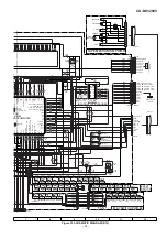
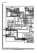
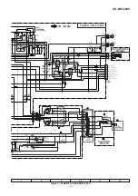
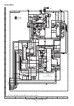
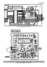

CD-BK3200V
– 34 –
A
B
C
D
E
F
G
H
1
2
3
4
5
6
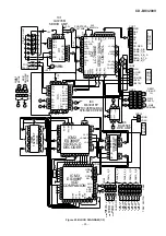
• NOTES ON SCHEMATIC DIAGRAM can be found on page 51.
Figure 34 SCHEMATIC DIAGRAM (7/12)
+B
+B
+B
+B
+B
+B
+B
+B
+B
+B
+B
+B
+B
+B
+B
+B
+B
+B
+B
65 64 63
61 60 59 58 57 56 55 54 53 52 51 50 49 48 47 46 45 44 43 42 41 40 39 38 37 36 35 34 33 32 31 30 29 28 27 26 25 24
1
19
18
17
16
15
14
13
12
11
10
9
8
7
6
5
4
3
2
1
100
99
98
97
96
95
94
93
92
91
90
89
88
87
86
85
84
83
82
82
81
81
50
49
48
32
31
44
43
42
41
40
39
38
37
36
35
34
34
22
22
21
20
19
18
17
16
15
14
13
12
12
23 24 25 26 27 28 29 30 31 32 33
11 10
9 8 7 6 5 4 3 2 1
80 79 78 77 76 75 7 4 73 72 71 70 69 68 67 66 65 64 63
16 17 18
2
1
3 4 5 6 7 8 9
10 11 12 13 14 15
MICIN
KLATCH
CEO
CLK
DI
DO
REC/PLAY
T_T1/T2
T_BIAS
–20DBATT
P13
P12
P11
P10
P1
P2
P3
P4
P6
P8
SPRLY
SP_DET
ANI1
ANI2
ANI3
ANI4
ANI5
P9
P7
P5
MICIN
G4
G5
G6
G9
G10
G11
G12
G13
G14
G15
G16
P22
P23
P24
P25
P26
P27
P28
P29
P30
P31
P32
P33
P34
P35
P36
P37
P38
P39
P40
P41
P41
P40
P39
P38
P37
P36
P35
P34
P33
P32
P31
P30
P29
P28
P27
P26
P25
P24
P23
P22
G16
G15
G14
G13
G12
G11
G10
G9
P1
P2
P3
P4
P5
P6
P7
P8
P9
P10
P14
P15
P16
P17
P18
P19
P20
P21
G1
G2
G3
G7
G8
KLATCH
BACK_UP
SO
+VF2
VF1
–VF
P_IN
UN_SW 5V
/SPEANA SEL C
/SPEANA SEL B
M_GND
KEY2
KEY1
RES
VPP
SI
D-GND
VDD
BG1
BG2
BG3
BG4
BG5
BG6
BG7
BG8
BS1
BS2
BS3
BS4
BS5
BS6
BS7
BS8
BS9
BS10
BS11
BS12
BS13
BS14
BS15
BS16
BS17
BS18
BS19
BS20
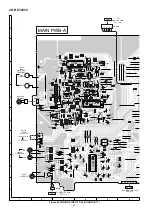
DISPLAY PWB-B1
AIN
SPN/TUN_SM
GND
AOUT
TEST
SEL
C
B
A
VCC
AIN
CIN
DIFOUT
RREF
VREFC
BIASC
STB
CLK
DIN
DOUT
OSC
VEE
VDD
VDD
VSS VSS
D_GND
A_+10V
+5V
M_+12V
100
FIP0
FIP1
FIP2
FIP3
FIP4
FIP5
FIP6
FIP7
FIP8
FIP9
FIP10
FIP11
FIP12
FIP13
FIP14
FIP15
FIP16
FIP17
FIP18/SPEANA SEL A
FIP19
VLOAD
VDD2
FIP20
FIP21
FIP22
FIP23
FIP24
FIP25
FIP26
FIP27
FIP28
DIST IN
MPEG_POW
KARAOKE LATCH
FL LATCH
MIC SW
JOG 1
JOG
0
DSA_STB
DSA_DATA
AC3_SCK/DS
TIMER LED
DO
VDD1
X2
X1
VSS1
AVSS
TUN_SM/SPN
T2RUN
T1RUN
KEY2
KEY1
KEY0
ANI5
ANI4
ANI3
ANI2
ANI1
AVDD
SPEANA
A OUT
9
8
7
6
5
4
3
2
1
9
8
7
6
5
4
3
2
1
6
5
4
3
2
1
16
19
2
1
3
4
5
6
7
8
9
10
11
12
13
14
15
17
18
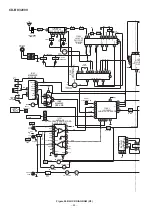
TO MAIN PWB
P33 10-H
TO POWER PWB
P36 1-F
CNP905
CNP602
RS701
1K
RS702
1K
C727 0.0015
R703
82K
R702
47K
R701
47K
C702
47/25
C701
0.022
IC702
D16315GB
FL DISPLAY
DRIVER
FL701
FL DISPLAY
C703
47/50
C705 47/25
R708
1K
R709 1K
R710 1K
R707 33
R704
100K
R705
100K
R706
100K
Q703
KTC3199 GR
Q702
KTC3199 GR
Q701
KTC3199 GR
R761 10K
R762 10K
R766 10K
R792 10K
R798 10K
C706
0.022
R727 1K
C714
220/10
C713
0.022
R717 10K
R716 10K
XL701
C712
15P
C711 18P
R719 1K
R724 1K
R725 1K
R726 1K
R728 1K
R729 1K
R723 1K
R722 1K
R721 1K
R720 1K
R712
47K
R713
10K
R714 10K
R715
10K
D711
DS1SS133
D713
DS1SS133
D712
DS1SS133
C709
0.1
C708 0.1
C707
0.1
C710
0.1
IC703
BA3835F
5 BAND PASS
FILTER
R711
100K
CNP702
D717
DS 1SS133
D716
DS1SS133
BI701
IC701
IX0413AW
SYSTEM MICROCOM
D708
DS1SS133
R775 1K
R745
10K
D701
DS1SS133
D703
DS1SS133
D705
DS1SS133
R776
10K
C704
0.022
R777
10K
R770 100
R771 100
R772 1K
R773 1K
R774 1K
R718 1K
CNS905
FFC702


