background image


SERVICE MANUAL

Parts marked with "

" are important for maintaining the safety of the set. Be sure to replace these parts with specified ones for maintaining the

safety and performance of the set.

This document has been published to be used for
after sales service only.
The contents are subject to change without notice.

SAFETY PRECAUTION

IMPORTANT SERVICE SAFETY 

PRECAUTION............................................................ i

PRECAUTIONS FOR USING LEAD-FREE 

SOLDER ................................................................... ii

CHAPTER 1. SPECIFICATIONS

[1] SPECIFICATIONS .................................................1-1

CHAPTER 2. OPERATION MANUAL

[1] OPERATION 

MANUAL ..........................................2-1

CHAPTER 3. DIMENSIONS

[1] DIMENSIONS ........................................................3-1

CHAPTER 4. REMOVING OF MAJOR PARTS

[1] 

REMOVING OF MAJOR PARTS (LC-42D85X) .....4-1

[2] 

REMOVING OF MAJOR PARTS (LC-46D85X) .....4-7

[3] 

REMOVING OF MAJOR PARTS (LC-52D85X) ...4-13

CHAPTER 5. ADJUSTMENT PROCEDURE

[1] ADJUSTMENT 

PROCEDURE ...............................5-1

CHAPTER 6. TROUBLESHOOTING TABLE

[1] TROUBLESHOOTING 

TABLE...............................6-1

CHAPTER 7. OVERALL WIRING/BLOCK DIAGRAM

[1] OVERALL 

WIRING 

DIAGRAM ..............................7-1

[2] SYSTEM 

BLOCK 

DIAGRAM .................................7-2

CHAPTER 8. PRINTED WIRING BOARD ASSEMBLIES

[1] MINI-AV 

Unit ..........................................................8-1

[2] 

R/C, LED Unit.........................................................8-2

[3] KEY 

Unit.................................................................8-3

[4] MAIN 

Unit...............................................................8-4

[5] SUB 

Unit ................................................................8-8

CHAPTER 9. SCHEMATIC DIAGRAM

[1] 

DESCRIPTION OF SCHEMATIC DIAGRAM .........9-1

[2] MINI-AV 

Unit ..........................................................9-2

[3] 

R/C, LED Unit.........................................................9-3

[4] KEY 

Unit.................................................................9-4

[5] MAIN 

Unit...............................................................9-5

[6] SUB 

Unit ..............................................................9-20

Parts Guide

TopPage

CONTENTS

In the interests of user-safety (Required by safety regulations in some countries) the set should
be restored to its original condition and only parts identical to those specified should be used

.

LCD COLOUR TELEVISION

No. S88P2LC52D85X

LC-42/46/52D85X

LC-42D85X

LC-46D85X

LC-52D85X

MODELS

Summary of Contents for AQUOS LC-42D85X

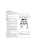
Page 1: ...85X 4 7 3 REMOVING OF MAJOR PARTS LC 52D85X 4 13 CHAPTER 5 ADJUSTMENT PROCEDURE 1 ADJUSTMENT PROCEDURE 5 1 CHAPTER 6 TROUBLESHOOTING TABLE 1 TROUBLESHOOTING TABLE 6 1 CHAPTER 7 OVERALL WIRING BLOCK DIAGRAM 1 OVERALL WIRING DIAGRAM 7 1 2 SYSTEM BLOCK DIAGRAM 7 2 CHAPTER 8 PRINTED WIRING BOARD ASSEMBLIES 1 MINI AV Unit 8 1 2 R C LED Unit 8 2 3 KEY Unit 8 3 4 MAIN Unit 8 4 5 SUB Unit 8 8 CHAPTER 9 SC...

Page 2: ...ds knobs and control shafts escutcheon etc and measure the AC voltage drop across the resistor All checks must be repeated with the AC cord plug connection reversed If necessary a nonpolarized adaptor plug must be used only for the purpose of completing these checks Any reading of 0 74 Vrms this corresponds to 0 5 mA rms AC or more is excessive and indicates a potential shock hazard which must be ...

Page 3: ...ad solder by 40 C and as it has poor solder wettability you may be apt to keep the soldering bit in contact with the PWB for extended period of time However Since the land may be peeled off or the maximum heat resistance temperature of parts may be exceeded remove the bit from the PWB as soon as you confirm the steady soldering condition Lead free solder contains more tin and the end of the solder...

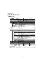
Page 4: ...576P 720P 50Hz 720P 60Hz 1080I 50Hz 1080I 60Hz 1080P 50Hz 1080P 60Hz 1080P 24Hz HDMI HDMI input 480I 576I 480P 576P 720P 50Hz 720P 60Hz 1080I 50Hz 1080I 60Hz 1080P 50Hz 1080P 60Hz 1080P 24Hz AUDIO in 15 pin mini D sub AUDIO in Ø 3 5 mm jack STEREO BILINGUAL NICAM B G I D K A2 stereo B G Resolution 2 073 600 pixels 1920 1080 As a part of policy of continuous improvement SHARP reserves the right to ...

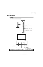
Page 5: ...indicator POWER On Off button MENU button OPC Optical Picture Control TV VIDEO button OPC sensor Remote control sensor POWER indicator The illustrations in this operation manual are for explanation purposes and may vary slightly from the actual operations The illustrations used throughout this manual are based on LC 42D85X TV Front Side SLEEP timer indicator ...

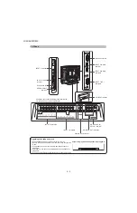
Page 6: ...not in use The speakers do not output volume when headphones are plugged in The Audio menu cannot be operated when headphones are plugged in You can set the volume to different levels for each input source Volume display when headphones are plugged in 20 Headphone jack INPUT 5 HDMI terminal INPUT 6 HDMI terminals INPUT 3 terminals MONITOR OUT terminals DIGITAL AUDIO OUTPUT terminal SERVICE ONLY te...

Page 7: ...ubpage directly Top Bottom Full TELETEXT mode Set the area of magnification 14 TV VIDEO INPUT SOURCE Select an input source TV INPUT 1 INPUT 2 INPUT 3 INPUT 4 INPUT 5 INPUT 6 INPUT 7 PC 15 FAV Display the favourite channel setting 16 RADIO Press to access RADIO mode 17 DISPLAY Displays the channel or input information DTV mode Displays the time information included in the DTV broadcast TELETEXT mo...

Page 8: ...e bottom of the TV Insert and tighten the 4 short screws into the 4 holes on the rear of the TV Hex key Short screw Soft cushion NOTE To detach the stand perform the steps in reverse order 2 Hex key Long screw Attach the supporting post for the stand unit onto the base as shown below Confirm the 8 screws supplied with the TV Short screws 4 used in step 3 Long screws 4 used in step 2 LC 42D85X LC 4...

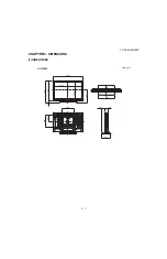
Page 9: ...LC 42 46 52D85X 3 1 LC 42 46 52D85X Service Manual CHAPTER 3 DIMENSIONS 1 DIMENSIONS 400 550 400 200 933 2 526 2 114 95 305 1004 409 708 646 62 Unit mm LC 42D85X ...

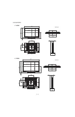
Page 10: ...LC 42 46 52D85X 3 2 550 400 400 1023 4 1101 575 6 62 434 124 95 325 175 760 698 Unit mm Unit mm LC 46D85X LC 52D85X 400 400 1157 0 1237 550 651 6 124 95 325 836 774 62 137 472 ...

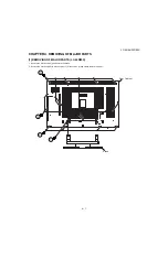
Page 11: ...e Manual CHAPTER 4 REMOVING OF MAJOR PARTS 1 REMOVING OF MAJOR PARTS LC 42D85X 1 Remove the 4 lock screws 1 and detach the Stand 2 Remove the 3 lock screws 2 4 lock screws 3 8 lock screws 4 and detach the Rear Cabinet Rear Cabinet 4 2 3 1 Stand ...

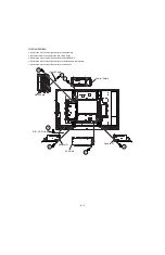
Page 12: ...ach the R C LED Unit 6 5 Remove the 4 lock screws 7 and detach the Control Shield 6 Remove the 9 lock screws 8 and detach the Ground Angle Main Shield 7 Remove the 6 lock screws 9 and detach the AV Shield 5 6 7 8 8 9 5 Speaker R R C LED Unit Speaker L RA Control Shield Main Shield Ground Angle AV Shield ...

Page 13: ...LC 42 46 52D85X 4 3 8 Disconnect all the connectors from all the PWBs 10 LP VD HM US KM LW SP PE KM PD LW LB LP RA U2 HM FE MA FE VD AC0 LA 1 LB LA R PE PL PD AC1 10 10 10 10 10 10 10 FR US ...

Page 14: ... AV Shield Side Key Cover from the Mini AV Angle 11 Detach the KEY Unit 14 from the Side Key Cover 12 Remove the 2 lock screws 15 and detach the Terminal Angle Bottom 13 Remove the 4 lock screws 16 and detach the Tray Chassis 16 16 15 Tray Chassis Terminal Angle Bottom 12 13 14 11 Mini AV Angle Side Key Cover MINI AV Unit Mini AV Shield Operation Button KEY Unit 11 ...

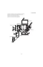
Page 15: ...rews 19 and detach the Main PWB Radiator MAIN Unit 16 Remove the 6 lock screws 20 and detach the SUB Unit 17 Remove the 5 lock screws 21 and detach the AC INLET Unit 18 Remove the 6 lock screws 22 and detach the POWER Unit 19 20 21 22 17 17 18 Terminal Angle Side POWER Unit MAIN Unit AC INLET Unit SUB Unit 19 Main PWB Radiator ...

Page 16: ...emove the 14 lock screws 23 and detach the Panel Support Angle 20 Remove the 2 lock screws 24 21 Remove the 8 lock screws 25 and detach the LCD Panel Module Panel Support Angle Panel Support Angle 23 23 24 25 LCD Panel Module ...

Page 17: ...2D85X 4 7 2 REMOVING OF MAJOR PARTS LC 46D85X 1 Remove the 4 lock screws 1 and detach the Stand 2 Remove the 2 lock screws 2 4 lock screws 3 8 lock screws 4 and detach the Rear Cabinet Stand 2 1 3 4 Rear Cabinet ...

Page 18: ...ach the R C LED Unit 6 5 Remove the 4 lock screws 7 and detach the Control Shield 6 Remove the 9 lock screws 8 and detach the Ground Angle Main Shield 7 Remove the 6 lock screws 9 and detach the AV Shield 5 6 5 Speaker L Speaker R R C LED Unit RA 7 Control Shield 9 AV Shield 8 8 Main Shield Ground Angle ...

Page 19: ...LC 42 46 52D85X 4 9 8 Disconnect all the connectors from all the PWBs 10 VD KM HM US LW LA 1 LA 2 LB 10 10 10 10 KM RA PD LW LB LP FE SP PE VD MA U2 HM FE AC0 LA R PE PD PL AC1 LA L 10 10 10 FR US ...

Page 20: ...ni AV Shield Side Key Cover from the Mini AV Angle 11 Detach the KEY Unit 14 from the Side Key Cover 12 Remove the 2 lock screws 15 and detach the Terminal Angle Bottom 13 Remove the 4 lock screws 16 and detach the Tray Chassis 11 16 16 15 12 14 13 Mini AV Angle Side Key Cover MINI AV Unit Mini AV Shield Operation Button KEY Unit Tray Chassis Terminal Angle Bottom ...

Page 21: ...rews 19 and detach the Main PWB Radiator MAIN Unit 16 Remove the 6 lock screws 20 and detach the SUB Unit 17 Remove the 5 lock screws 21 and detach the AC INLET Unit 18 Remove the 6 lock screws 22 and detach the POWER Unit 19 20 21 22 17 17 18 Terminal Angle Side POWER Unit MAIN Unit AC INLET Unit SUB Unit 19 Main PWB Radiator ...

Page 22: ...6 52D85X 4 12 19 Remove the 14 lock screws 23 and detach the Panel Support Angle 20 Remove the 8 lock screws 24 and detach the LCD Panel Module Panel Support Angle LCD Panel Module 24 23 23 Panel Support Angle ...

Page 23: ...2D85X 4 13 3 REMOVING OF MAJOR PARTS LC 52D85X 1 Remove the 4 lock screws 1 and detach the Stand 2 Remove the 3 lock screws 2 4 lock screws 3 8 lock screws 4 and detach the Rear Cabinet 1 Stand 2 3 4 Rear Cabinet ...

Page 24: ...tach the R C LED Unit 6 5 Remove the 4 lock screws 7 and detach the Control Shield 6 Remove the 9 lock screws 8 and detach the Ground Angle Main Shield 7 Remove the 6 lock screws 9 and detach the AV Shield 5 6 5 Speaker L Speaker R R C LED Unit RA 7 8 8 Control Shield 9 AV Shield Main Shield Ground Angle ...

Page 25: ...LC 42 46 52D85X 4 15 8 Disconnect all the connectors from all the PWBs 10 LA 1 VD HM US KM LA 2 LB LW 10 10 10 KM RA PD LW LB LP FE SP PE VD MA U2 HM FE AC0 LA R PE PD PL AC1 LA L 10 10 10 FR US ...

Page 26: ...ni AV Shield Side Key Cover from the Mini AV Angle 11 Detach the KEY Unit 14 from the Side Key Cover 12 Remove the 2 lock screws 15 and detach the Terminal Angle Bottom 13 Remove the 4 lock screws 16 and detach the Tray Chassis 11 16 16 15 12 14 13 Tray Chassis Terminal Angle Bottom Mini AV Angle Side Key Cover MINI AV Unit Mini AV Shield Operation Button KEY Unit ...

Page 27: ...rews 19 and detach the Main PWB Radiator MAIN Unit 16 Remove the 6 lock screws 20 and detach the SUB Unit 17 Remove the 5 lock screws 21 and detach the AC INLET Unit 18 Remove the 6 lock screws 22 and detach the POWER Unit 19 20 21 22 17 17 18 Terminal Angle Side POWER Unit MAIN Unit AC INLET Unit SUB Unit 19 Main PWB Radiator ...

Page 28: ...6 52D85X 4 18 19 Remove the 14 lock screws 23 and detach the Panel Support Angle 20 Remove the 8 lock screws 24 and detach the LCD Panel Module Panel Support Angle LCD Panel Module 24 23 23 Panel Support Angle ...

Page 29: ...leted with OK displayed 3 After replacing the LCD panel or LCD control PWB adjust the VCOM in the following procedure 1 Enter the process adjustment mode 2 Use the cursor keys and CH of R C to select the item VCOM ADJ on the page 9 32 3 Press the ENTER key to verify that the adjustment pattern is displayed 4 Use the keys of VOL of L C to adjust the flicker in the center of the screen to minimum 5 ...

Page 30: ...ignal is available 4 Description of display CAUTION Use due care in handling the information described here lest the users should know how to enter the adjustment process mode If the settings are tampered with in this mode unrecoverable system damage may result Remote controller key Main unit key Function CH CH Moving an item line by one UP DOWN VOL VOL Changing a selected item setting 1 1 Cursor ...

Page 31: ...C YPOS 0 Y coordinate setting for VIC READ 12 VIC SIGNAL TYPE MAIN Signal type setting for VIC READ 13 VIC READ OFF Picture level acquisition function Level appears in green on the upper right 3 32 TUNER ADJ 1 RF AGC ADJ Enter RF AGC auto adjustment execution 2 TUNER ADJ Enter TUNER auto adjustment execution 3 PAL TUNER ADJ Enter PAL TUNER auto adjustment execution 4 RF AGC ADJ CA 8CH Enter RF AGC...

Page 32: ...DDR BIST Enter 11 32 LEV 1 LEV1 176 2 LEV2 352 3 LEV3 528 4 LEV4 656 5 LEV5 800 6 LEV6 928 12 32 MGXX1 1 MG1R 178 W B adjustment gradation 1R adjustment value 2 MG1G 184 W B adjustment gradation 1G adjustment value 3 MG1B 138 W B adjustment gradation 1B adjustment value 4 MG2R 227 W B adjustment gradation 2R adjustment value 5 MG2G 232 W B adjustment gradation 2G adjustment value 6 MG2B 177 W B ad...

Page 33: ...DJUSTER2 9 GAIN_ADJUSTER3 10 GAIN_ADJUSTER4 11 GAIN_ADJUSTER5 12 GAIN_ADJUSTER6_SP 13 GAIN_ADJUSTER6_HP 17 32 SOUND 3 1 LOUT1_VOLUME_CONTROL 2 ROUT1_VOLUME_CONTROL 18 32 M PWM 1 PWM 2 PWM FREQ 3 PWM DUTY 4 OSC FREQ 5 OSC DUTY 19 32 M OPC1 1 OPC LDUTY0 2 OPC LDUTY1 3 OPC LDUTY2 4 OPC LDUTY3 5 OPC LDUTY4 6 OPC LDUTY5 7 OPC LDUTY6 8 OPC LDUTY7 9 OPC LDUTY8 10 OPC LDUTY9 11 OPC LDUTY10 12 OPC LDUTY11 ...

Page 34: ...L 12 2 OPC33 ADLEVEL 13 3 OPC33 ADLEVEL 14 4 OPC33 ADLEVEL 15 5 OPC33 ADLEVEL 16 6 OPC33 ADLEVEL 17 7 OPC33 ADLEVEL 18 8 OPC33 ADLEVEL 19 9 OPC33 ADLEVEL 20 10 OPC33 ADLEVEL 21 11 OPC33 ADLEVEL 22 24 32 M ADL3 1 OPC33 ADLEVEL 23 2 OPC33 ADLEVEL 24 3 OPC33 ADLEVEL 25 4 OPC33 ADLEVEL 26 5 OPC33 ADLEVEL 27 6 OPC33 ADLEVEL 28 7 OPC33 ADLEVEL 29 8 OPC33 ADLEVEL 30 9 OPC33 ADLEVEL 31 25 32 M V6THE 1 V6 ...

Page 35: ...MEM CLEAR 1 KEY LOCK 1217 Enter 2 KOUTEI AREA ALL CLEAR Adjustment value clearness in all areas in process 3 A MODE AREA CLEAR Adjustment value clearness of process A mode 4 BACKUP AREA CLEAR Adjustment value clearness in process backup area 5 B MODE AREA CLEAR Adjustment value clearness of process B mode 6 EXECUTION Clear execution 31 32 FR REGI 1 READ WRITE READ 2 SLAVE ADDRESS SLAVE0 3 REGISTOR...

Page 36: ...phenomenon 1 occurs 5 times consecutively it becomes impossible to turn on the power The power LED remained red 2 Measures 1 Checking with lamp error detection OFF Enter the adjustment process mode referring to 1 Entering and exiting the adjustment process mode If there is a problem with the lamp or lamp circuit the lamp will go out The power LED is green Then you can check the operation to see if...

Page 37: ...mmunication from main CPU 3 times 1 time 03 Initial Communication Error 3 Receive initial communication only 3 times 2 times 04 Initial Communication Error 4 To the communication setting reception 3 times 2 times 05 Initial Communication Error 5 To the initialization completion reception 3 times 2 times 06 Initial Communication Error 6 To the notice of version reception 3 times 2 times 07 Initial ...

Page 38: ...imes 21 Power supply Error 5 Panel Power Error 2 times 5 times 22 Power supply Error 6 Not used 23 Main micom Error Error Standby request from Main CPU 2 times 7 times 24 Power supply Error 7 AC_DET Error during power on sequence 2 times 1 time Display Error Reason Power RED LED Blink Times OPC LED Blink Times ...

Page 39: ... position and shift the input position rightward one digit When three digits are completely input the Pass Word is judged c Check the Pass Word by inputting three digits If the Pass Word is it shifts to the PUBLIC Mode setting screen In another case the screen is erased and it operates in the ordinary mode 2 Exiting the Public Mode screen There are two following ways to exit the Public Mode settin...

Page 40: ...ecision ENTER Execution Used by the items Execution and RESET PUBLIC Mode R C Ordinary operation mode It enters the PUBLIC Mode PUBLIC MODE Flag is set to ON PUBLIC Mode It exits the PUBLIC Mode PUBLIC MODE Flag does not change Any set item in PUBLIC Mode is not initialized Public Mode POWER ON FIXED VARIABLE SHUT DOWN MODE NORMAL MAXIMUM VOLUME 60 VOLUME FIXED VARIABLE VOLUME FIXED LEVEL 20 RC BU...

Page 41: ...e speakers of the main unit Exception Remarks When it is set to 59 or less the number is displayed and the volume bar is not displayed during operation in the ordinary mode VOLUME can be abbreviated to VOL Selection VARIABLE or FIXED is selectable Loop is provided Default VARIABLE Function It is selectable whether or not the volume is fixed to the value adjusted in the volume fixed level mode Only...

Page 42: ... the setting contents the start operation of the process mode inspection mode and PUBLIC_Mode is enabled Regardless of the setting contents all keys can be used while entering the process mode inspection mode or PUBLIC_Mode Key that becomes invalid excluding Default besides MENU Key because of setting ON_TIMER Auto Preset Manual_Memory and clock setting All Direct Shift keys to the MENU display Re...

Page 43: ...elect and Direct input switching Remarks When START MODE is set to NORMAL this item is disable to set Automatically set to VARIABLE When set to FIXED The Channel setting MENU Menu setup Auto Installation Programme setup and Child Lock item hatching and Input Selection MENU in MENU are not displayed Composite signal PAL 0 7Vp p 0 02Vp p Pedestal to white level RGB signal 0 7Vp p 0 02Vp p 15K compon...

Page 44: ...when finished Adjustment point Adjustment Conditions Adjustment procedure 1 Setting Signal SECAM Full Field Colour Bar signal Terminal INPUT1 VIDEO IN Feed the SECAM full field colour bar signal 75 colour saturation to INPUT1 VIDEO INPUT 2 Auto adjustment performance Page 4 32 Bring the cursor on SECAM ADJ and press ENTER SECAM ADJ OK appears when finished Adjustment point Adjustment Conditions Ad...

Page 45: ...justment procedure 1 Setting Signal COMP33K 50Hz 1080i 100 Full Field Colour Bar sig nal Terminal INPUT1 COMPONENT INPUT Feed the COMPONENT 33K 100 1080i full field colour bar signal 100 colour saturation to INPUT1 COMPONENT INPUT 2 Auto adjustment performance Page 7 32 Bring the cursor on HDTV ADJ and press ENTER HDTV ADJ OK appears when finished Adjustment point Adjustment Conditions Adjustment ...

Page 46: ...display Change MG5R MG5B adjustment offset value on page 13 32 of process adjustment so that the values of the luminance meter approach x 0 272 and y 0 277 5 Repeat step 4 for points 4 3 2 and 1 Adjustment reference standard value Adjustment spec 0 002 Inspection spec 0 004 point 1 and 2 Adjustment spec 0 001 Inspection spec 0 002 Excluding the above mentioned Adjusting procedure by use of RS 232C...

Page 47: ...aduation 5 0000 4095 LEV40656 Graduation 4 656 graduation adjustment MG4G Adjustment of G of graduation 4 Calculated value MG4R Adjustment of R of graduation 4 0000 4095 MG4B Adjustment of B of graduation 4 0000 4095 LEV30528 Graduation 3 528 graduation adjustment MG3G Adjustment of G of graduation 3 Calculated value MG3R Adjustment of R of graduation 3 0000 4095 MG3B Adjustment of B of graduation...

Page 48: ...nt process mode are not initialized Keep this in mind when initializing these settings Adjustment item Adjustment conditions Adjustment procedure 1 Factory settings ends by turning off the MAIN POWER key See to below caution Factory setting with adjustment process mode Enter the adjustment process mode Move the cursor to INDUSTRY INIT on page 2 32 EXECUTING display appears After a while SUCCESS di...

Page 49: ...upgraded Finally the main version number appears on screen 7 Turn off the AC power Unplug the AC power cord Take out the upgrading USB flash memory 8 Now the software has been upgraded NOTE Then get the set started and call the process adjustment screen 1 32 to check the main software version CAUTION 1 Do not take out and put in the USB flash memory during formatting 2 It takes about one minute to...

Page 50: ...he PS ON signal and PNL POWsignal input at pin 4 and 6 of P9601 NO Check the PS ON signal line PNL POW signal line YES Is the output voltage of each pin on P9601 as prescribed pin8 5V pin11 and 12 15V NO Replace the power unit RDENCA237WJQZ and ac inlet unit RUNTKA341WJQZ YES Are the DC DC converter outputs and the output voltages along the control line SUB 5V IC402 Q402 1 5V IC403 9V IC404 B3 3 I...

Page 51: ... its peripheral circuits YES Check Speaker Box right and left and wire harness No sound during the reception of TV ANALOG broadcasting Does not the sound go out though the picture has come out when UHF VHF is received SUB UNIT Is the IF signal output from pin 17 of TUNER TU7501 NO Check the tuner and its peripheral circuits Replace as required YES Is the SIF signal sent to pins 23 and 24 of IC7504...

Page 52: ...put devices 1 Does not the sound of the audio signal input to INPUT1 go out Does not the sound of the audio signal input to INPUT2 go out SUB UNIT INPUT1 Is the audio signal properly sent to pins 5 IN1_L and 4 IN1_R of INPUT1 J1704 NO Check the setting of an external input device that connects of J1704 INPUT2 Is the audio signal properly sent to pins 5 IN2_L and 4 IN2_R of INPUT2 J1702 NO Check th...

Page 53: ...d external devices YES Is V3_PLUG signal input to pin 2 of IC506 VIDEO SELEC TOR NO Everything from V3_PLUG_LINE J901 to pin 2 of IC506 is checked connector P901 P501 and etc YES Refer to No sound output in all modes No sound from external input devices 3 Does not the sound of the audio signal input to INPUT4 5 6 HDMI go out Is picture of the signal input from INPUT4 5 6 displayed NO Refer to Does...

Page 54: ...SUB UNIT YES NO Check the line between IC1504 and SC1101 and their peripheral circuits Is audio signal HDMI_PC_L MAIN_L HDMI_PC_R MAIN_R sent to pins 24 and 26 of SC501 NO Check the connector SC1101 SC501 YES Is audio signal input to pin 59 MAIN_L and 60 MAIN_R of IC1404 CODEC NO Check the line between P501 and IC1404 YES Refer to No sound output in all modes The audio signal is not output 1 No au...

Page 55: ...N_UNIT s IC9101 CPLD from pin 6 of a headphone terminal J802 NO Check the line between J802 and IC9101 P801 P1101 IC9105 etc YES Is the audio signal output to pin 2 L pin 3 R of headphone ter minal J802 YES Check HEAD PHONE J802 or peripheral circuits MAIN UNIT NO Is the audio signal input into pin 5 and 7 of connector P1101 from pin 6 L 4 R of Q2404 YES Check the line between P1101 and J802 P801 ...

Page 56: ...ignal input to connector SC4801 XL2E CN4804 X20E of the panel module NO Wire harness LW is checked YES Check the panel module No picture on the display 2 Does not the picture come out when VHF UHF is received SUB UNIT Is IF signal output from pin 17 of TUNER TU7501 NO Check whether I2C is normally accessed between named TU7501 and IC7507 COFDM YES Is IF signal input to pin 1 and 2 of IC7504 IF DEM...

Page 57: ...D_D of a con nector P7501 and pin 51 FESTR_PSYNC 50 FEVAL_DEN of a connector SC501 NO Is the control signal named IC7507 and IC9101 CPLD normal FE_RST_LINE FEERR_LINE FEPG0_COMP_LINE FEPG1_LOCK_LINE etc MAIN UNIT YES Is the digital signal input into pin 1 FECLK 3 FED_D of a con nector P1103 and pin 51 FESTR_PSYNC 50 FEVAL_DEN of a connector SC1101 NO Connector SC501 SC1101 and P7501 P1103 are chec...

Page 58: ...external input device that connects of J1702 YES INPUT1 Is CVBS signal sent to pin 65 of IC506 NO Check the line between J1704 and IC506 INPUT2 Is CVBS signal sent to pin 71 of IC506 NO Check the line between J1702 and IC506 YES Is Y C signal output to pin 2 of connector SC501 from pin 52 of IC506 NO Check the line between IC506 and SC501 MAIN UNIT YES Is CVBS signal MAIN_Y V input to pin 2 of con...

Page 59: ...nt to pins 27 Y 29 Pb and 31 Pr of IC506 NO Check the line between J1703 and IC506 YES INPUT1 Is detection signal COMP1_PLUG of the COMPONENT video signal from pin 7 of the input terminal J1705 normal NO Check from the input terminal J1705 to pin 38 of IC506 INPUT2 Is detection signal COMP2_PLUG of the COMPONENT video signal from pin 7 of the input terminal J1703 normal NO Check from the input ter...

Page 60: ...e video signal detection signal V3_PLUG signal from pin 7 of the input terminal J901 normal NO Check J901 or peripheral circuits YES Is the V3_PLUG signal input to pin 2 of IC506 NO Check the between V3_PLUG_LINE J901 and pin 2 of SUB UNIT s IC506 ConnectorP901 P501 etc YES Is video signal MAIN_Y V output into pin 2 of connector SC501 from pin 52 of IC506 NO Check the line between IC506 and SC501 ...

Page 61: ...he Y C video signal detection function S3_PLUG signal from pin 6 of the input terminal J902 normal NO Check J902 or peripheral circuits YES Is the S3_PLUG signal input to pin 42 of IC506 NO Check the between S3_PLUG_LINE J902 and pin 42 of SUB UNIT s IC506 connector P901 P501 etc YES Is Y C signal output into pin 2 4 of connector SC501 from pin 52 Y 50 C of IC506 NO Check the line between IC506 an...

Page 62: ...FER of IC803 from SC801 NO Check the line between SC801 and IC803 YES Is TMDS signal output into pin 11 12 8 9 5 6 2 3 of the connector SC802 from pin 8 9 CLK 6 7 DAT0 3 4 DAT1 1 2 DAT2 of IC803 NO Check the line between IC803 and SC802 YES Is TMDS signal input into pin 59 58 TMDS6_CLK 62 61 TMDS6_D0 65 64 TMDS6_D1 68 67 TMDS6_D2 of IC1507 NO Check the line between connector SC802 and IC1507 SC802...

Page 63: ...f IC1502 EEPROM accessed and is it read from pin 15 16 of a HDMI terminal SC1501 pin 15 16 NO Is access possible in the re writing or exchange of EDID data of IC1502 NO Check the circumference circuit of SC1501 IC1501and IC1507 YES INPUT5 Is TMDS signal input into pin 19 18 TMDS2_CLKP N 22 21 TMDS2_D0P N 25 24 TMDS2_D1P N 28 27 TMDS2_D2P N of IC1507 from SC1501 NO Check the line between SC1501 and...

Page 64: ...ized signal input from pin 1 2 3 R G B 13 and 14 V H of input terminal D SUB SC1504 YES Check the connection and setup between SC1504 and its cir cumference circuit as well as the external HDMI devices IC1503 etc NO Are the video signal and the synchronized signal input from pin U8 Y7 W10 R G B pin V10 U10 H V of IC3301 VIDEO PROCESSOR YES Check the line between SC1504 and IC3301 NO Refer to The p...

Page 65: ...7504 FL7502 VIF_SAW and its peripheral circuits NO Check whether I2C is normally accessed between TU7501 and IC7507 COFDM During external connection No picture on the monitor 2 No picture appears on MONITOR OUT1 connected monitor during the tuner DTV reception Checklist 1 Is ANT CABLE disconnected or connected improperly Connect it correctly as per the operation manual 2 The picture is sent to the...

Page 66: ...or picture is not sent and is not displayed on the monitor refer to No picture for each terminal SUB UNIT Is CVBS signal input from pin 51 of IC506 to pin 6 of J1701 YES Check the setting of an external input device that connects of J1701 NO Is CVBS signal sent to pin INT_V 65 or IN2_V 71 of IC506 VIDEO_SELECTOR YES Check the IC506 and its peripheral circuits NO Is CVBS signal sent to pin 8 of INP...

Page 67: ...C506 in the SUB UNIT Connector P901 P501 etc LED flashing patterns for error notification 1 Power red LED Remarks Error type Power red LED operation 1 cycle Description Lamp failure Flashes once Fast ERR_PNL IC2002_43pin Abnormal L Confirmed after 5 consecutive detec tions at 1 second intervals detected during backlight light on Note that after five detection counts the lamp cannot be activated ex...

Page 68: ...or The details are displayed on page 1 of process adjustment for the main microprocessor IC8101 3 Communication failure details Power LED flashes 3 times and OPC LED flashes Remarks Error type OPC LED operation 1 cycle Description Initial communication reception failure Flashes once Initial communication from the main CPU IC8101 is not received Communication line failure or main CPU IC8101 start u...

Page 69: ...LC 42 46 52D85X 7 1 LC 42 46 52D85X Service Manual CHAPTER 7 OVERALL WIRING BLOCK DIAGRAM 1 OVERALL WIRING DIAGRAM A C B D E F G I H 1 2 3 4 5 6 7 8 9 10 11 12 13 14 15 16 17 18 19 20 21 22 ...

Page 70: ...LC 42 46 52D85X 7 2 2 SYSTEM BLOCK DIAGRAM A C B D E F G I H 1 2 3 4 5 6 7 8 9 10 11 12 13 14 15 16 17 18 19 20 21 22 T35DT13K T35DT13K CS35D32G T7L2 2Z Q 5 1 2 T35DT13K ...

Page 71: ... C810 C811 C812 Q805 LUG901 Q804 R818 R811 IC803 C804 C824 C817 C801 C823 D808 IC805 IC801 R832 C821 C820 R804 R806 R840 Q806 R809 C830 Q807 C822 R839 R829 L808 L807 L806 L805 L809 C826 C825 FB805 D809 IC806 P801 SC802 LUG902 IC804 R813 D807 R828 C829 R827 R826 R825 R824 Q803 C819 C818 R817 v1 IC807 FB802 R805 C805 C813 C814 C815 C809 C808 C807 C806 C903 VA807 VA803 VA804 R910 R909 D803 C904 R908 ...

Page 72: ...nit Side A R C LED Unit Side A Chip 3 R101 C107 C102 SLD101 RMC101 D101 R132 IC101 C105 C104 R136 R135 R102 R105 D103 R117 R137 R108 Q104 R109 R104 R107 Q102 Q103 D114 R138 R106 Q105 R121 R126 R110 R123 Q106 D115 R127 R122 Q107 R124 C110 C108 C101 R103 RMC102 R119 R120 D116 IC102 R116 R118 C103 C111 P101 R139 R140 P102 ...

Page 73: ... 52D85X 8 3 3 KEY Unit A C B D E F G I H 1 2 3 4 5 6 7 8 9 10 11 12 13 14 15 16 17 18 19 20 21 22 KEY Unit Side A KEY Unit Side A Chip S155 R153 D152 S154 S152 R151 D151 S151 R152 S153 R154 S156 S157 D155 P151 ...

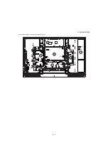
Page 74: ...LC 42 46 52D85X 8 4 4 MAIN Unit A C B D E F G I H 1 2 3 4 5 6 7 8 9 10 11 12 13 14 15 16 17 18 19 20 21 22 MAIN Unit Side A ...

Page 75: ...IC8704 R8131 R3311 R8132 R3506 R3507 R8710 IC3501 R3509 R8135 IC3502 R8136 R8137 R8714 R8138 R8139 R8718 C3539 R8332 R3512 R8333 R3514 R8140 J1501 R8141 R3516 J1502 R8142 R8143 R8144 P4501 R8145 P4502 R8147 R8148 R8149 C3548 LUG1101 R3521 R8729 LUG1102 C8176 C9116 C3357 LUG1103 R3524 LUG1104 R3525 C8179 LUG1105 R3526 R8152 R3527 R8153 R3528 R8154 Q1801 C8180 Q1804 R3530 C8379 R3532 P2001 R3341 SC1...

Page 76: ...LC 42 46 52D85X 8 6 A C B D E F G I H 1 2 3 4 5 6 7 8 9 10 11 12 13 14 15 16 17 18 19 20 21 22 MAIN Unit Side B ...

Page 77: ...TL1134 TL9604 C3338 C8159 C3339 TL1135 TL9605 TL9606 TL1136 R3312 R8133 TL1137 TL9607 C8350 TL1520 TL1138 TL9608 R3314 C8351 C3531 TL4401 TL1521 TL9609 R3315 TL1139 TL4402 C8352 C3532 R8712 TL1522 R3316 R8713 C3533 C8353 TL4403 TL1523 R3317 TL4404 C3534 C8354 TL1524 C8160 C3340 R3318 C3535 C8355 TL4405 TL1525 C8161 C9101 R3319 C3341 C8356 TL4406 TL1526 C8162 C3342 C8357 C3537 TL4407 TL1527 C8163 C...

Page 78: ...LC 42 46 52D85X 8 8 5 SUB Unit A C B D E F G I H 1 2 3 4 5 6 7 8 9 10 11 12 13 14 15 16 17 18 19 20 21 22 SUB Unit Side A ...

Page 79: ...309 R1301 D1301 Q1303 D1302 LF1 C1304 R1310 C422 IC404 FB404 C423 R430 C424 R431 FB406 FB405 C434 C414 C411 C406 FB402 IC402 C407 Q402 C432 R7512 IC405 D7503 R7530 C7519 R7506 L402 D7504 C7516 C429 R7517 D7506 C430 FL7501 FL7502 R7521 C7523 C420 C417 C403 D412 R433 C404 R7524 C7530 D410 C7525 R7522 C7524 C7533 D411 R432 D409 IC7504 IC403 C7528 R7520 C401 C7542 R1467 R1460 R7526 R1463 FB401 R7529 C...

Page 80: ...LC 42 46 52D85X 8 10 A C B D E F G I H 1 2 3 4 5 6 7 8 9 10 11 12 13 14 15 16 17 18 19 20 21 22 SUB Unit Side B ...

Page 81: ...stors are 5 unless otherwise noted K 10 F 1 D 0 5 3 All resistors are 1 16W unless otherwise noted CAPACITOR 1 All capacitors are µF unless otherwise noted P pF µµF 2 All capacitors are 50V unless otherwise noted CAUTION This circuit diagram is original one therefore there may be a slight difference from yours SAFETY NOTES 1 DISCONNECT THE AC PLUG FROM THE AC OUTLET BEFORE REPLACING PARTS 2 SEMICO...

Page 82: ...LC 42 46 52D85X 9 2 2 MINI AV Unit A C B D E F G I H 1 2 3 4 5 6 7 8 9 10 11 12 13 14 15 16 17 18 19 20 21 22 ...

Page 83: ...LC 42 46 52D85X 9 3 3 R C LED Unit A C B D E F G I H 1 2 3 4 5 6 7 8 9 10 11 12 13 14 15 16 17 18 19 20 21 22 ...

Page 84: ...LC 42 46 52D85X 9 4 4 KEY Unit A C B D E F G I H 1 2 3 4 5 6 7 8 9 10 11 12 13 14 15 16 17 18 19 20 21 22 ...

Page 85: ...LC 42 46 52D85X 9 5 5 MAIN Unit MAIN Unit 1 17 On this model the Main Circuit Basic Diagram 3 17 14 17 is not applied A C B D E F G I H 1 2 3 4 5 6 7 8 9 10 11 12 13 14 15 16 17 18 19 20 21 22 ...

Page 86: ...LC 42 46 52D85X 9 6 MAIN Unit 2 17 A C B D E F G I H 1 2 3 4 5 6 7 8 9 10 11 12 13 14 15 16 17 18 19 20 21 22 ...

Page 87: ...LC 42 46 52D85X 9 7 MAIN Unit 4 17 A C B D E F G I H 1 2 3 4 5 6 7 8 9 10 11 12 13 14 15 16 17 18 19 20 21 22 ...

Page 88: ...LC 42 46 52D85X 9 8 MAIN Unit 5 17 A C B D E F G I H 1 2 3 4 5 6 7 8 9 10 11 12 13 14 15 16 17 18 19 20 21 22 ...

Page 89: ...LC 42 46 52D85X 9 9 MAIN Unit 6 17 A C B D E F G I H 1 2 3 4 5 6 7 8 9 10 11 12 13 14 15 16 17 18 19 20 21 22 ...

Page 90: ...LC 42 46 52D85X 9 10 MAIN Unit 7 17 A C B D E F G I H 1 2 3 4 5 6 7 8 9 10 11 12 13 14 15 16 17 18 19 20 21 22 ...

Page 91: ...LC 42 46 52D85X 9 11 MAIN Unit 8 17 A C B D E F G I H 1 2 3 4 5 6 7 8 9 10 11 12 13 14 15 16 17 18 19 20 21 22 ...

Page 92: ...LC 42 46 52D85X 9 12 MAIN Unit 9 17 A C B D E F G I H 1 2 3 4 5 6 7 8 9 10 11 12 13 14 15 16 17 18 19 20 21 22 ...

Page 93: ...LC 42 46 52D85X 9 13 MAIN Unit 10 17 A C B D E F G I H 1 2 3 4 5 6 7 8 9 10 11 12 13 14 15 16 17 18 19 20 21 22 ...

Page 94: ...LC 42 46 52D85X 9 14 MAIN Unit 11 17 A C B D E F G I H 1 2 3 4 5 6 7 8 9 10 11 12 13 14 15 16 17 18 19 20 21 22 ...

Page 95: ...LC 42 46 52D85X 9 15 MAIN Unit 12 17 A C B D E F G I H 1 2 3 4 5 6 7 8 9 10 11 12 13 14 15 16 17 18 19 20 21 22 ...

Page 96: ...LC 42 46 52D85X 9 16 MAIN Unit 13 17 A C B D E F G I H 1 2 3 4 5 6 7 8 9 10 11 12 13 14 15 16 17 18 19 20 21 22 ...

Page 97: ...LC 42 46 52D85X 9 17 MAIN Unit 15 17 A C B D E F G I H 1 2 3 4 5 6 7 8 9 10 11 12 13 14 15 16 17 18 19 20 21 22 ...

Page 98: ...LC 42 46 52D85X 9 18 MAIN Unit 16 17 A C B D E F G I H 1 2 3 4 5 6 7 8 9 10 11 12 13 14 15 16 17 18 19 20 21 22 ...

Page 99: ...LC 42 46 52D85X 9 19 MAIN Unit 17 17 A C B D E F G I H 1 2 3 4 5 6 7 8 9 10 11 12 13 14 15 16 17 18 19 20 21 22 ...

Page 100: ...LC 42 46 52D85X 9 20 6 SUB Unit SUB Unit 1 5 A C B D E F G I H 1 2 3 4 5 6 7 8 9 10 11 12 13 14 15 16 17 18 19 20 21 22 ...

Page 101: ...LC 42 46 52D85X 9 21 SUB Unit 2 5 A C B D E F G I H 1 2 3 4 5 6 7 8 9 10 11 12 13 14 15 16 17 18 19 20 21 22 ...

Page 102: ...LC 42 46 52D85X 9 22 SUB Unit 3 5 A C B D E F G I H 1 2 3 4 5 6 7 8 9 10 11 12 13 14 15 16 17 18 19 20 21 22 ...

Page 103: ...LC 42 46 52D85X 9 23 SUB Unit 4 5 A C B D E F G I H 1 2 3 4 5 6 7 8 9 10 11 12 13 14 15 16 17 18 19 20 21 22 ...

Page 104: ...LC 42 46 52D85X 9 24 SUB Unit 5 5 A C B D E F G I H 1 2 3 4 5 6 7 8 9 10 11 12 13 14 15 16 17 18 19 20 21 22 ...

Page 105: ...C 46D85X LC 52D85X MODELS PartsGuide 1 PRINTED WIRING BOARD ASSEMBLIES 2 LCD PANEL 3 DUNTKE188FM05 MINI AV Unit 4 DUNTKE264FM03 R C LED Unit 5 DUNTKE266FM03 KEY Unit 6 DUNTKE976FM01 LC 42D85X DUNTKE976FM02 LC 46D85X DUNTKE976FM03 LC 52D85X MAIN Unit 7 DUNTKE977FM01 SUB Unit 8 CABINET AND MECHANICAL PARTS LC 42D85X 9 LCD PANEL UNIT LC 42D85X 10 CABINET AND MECHANICAL PARTS LC 46D85X 11 LCD PANEL UN...

Page 106: ...AB J Capacitor 0 1 10V Ceramic C812 VCKYCZ1HB102KY AB J Capacitor 1000p 50V Ceramic C813 RC KZA237WJZZY AB J Capacitor 10 16V Ceramic C814 VCKYCZ1HB102KY AB J Capacitor 1000p 50V Ceramic C815 VCKYCZ1AB104KY AB J Capacitor 0 1 10V Ceramic C816 VCKYCY1HB223KY AA J Capacitor 0 022 50V Ceramic C817 VCKYCZ1HB102KY AB J Capacitor 1000p 50V Ceramic C818 VCKYCZ1HB102KY AB J Capacitor 1000p 50V Ceramic C81...

Page 107: ...474JY AA J Resistor 470k 1 16W Metal Oxide R829 VRS CJ1JF100JY AA J Resistor 10 1 16W Metal Oxide R830 VRS CZ1JF102JY AA J Resistor 1k 1 16W Metal Oxide R831 VRS CZ1JF103JY AA J Resistor 10k 1 16W Metal Oxide R832 VRS CZ1JF103JY AA J Resistor 10k 1 16W Metal Oxide R834 VRS CZ1JF102JY AA J Resistor 1k 1 16W Metal Oxide R838 VRS CZ1JF472JY AA J Resistor 4 7k 1 16W Metal Oxide R839 VRS CZ1JF101JY AA ...

Page 108: ...95WJZZY AB J Capacitor 10 10V Ceramic C1509 VCKYCZ1HB221KY AA J Capacitor 220p 50V Ceramic C1510 VCKYCZ1HB102KY AB J Capacitor 1000p 50V Ceramic C1511 VCKYCZ1HB102KY AB J Capacitor 1000p 50V Ceramic C1512 VCKYTV1CB105KY AC J Capacitor 1 16V Ceramic C1513 VCKYTV1CB105KY AC J Capacitor 1 16V Ceramic C1514 VCERML1CN106MY AC J Capacitor 10 16V Electrolytic C1515 VCKYCZ1CF104ZY AA J Capacitor 0 1 16V C...

Page 109: ... C2613 VCKYCZ1AF104ZY AB J Capacitor 0 1 10V Ceramic C2614 VCKYCZ1HB221KY AA J Capacitor 220p 50V Ceramic C2615 VCKYCZ1HB221KY AA J Capacitor 220p 50V Ceramic C2616 VCKYCZ1AF104ZY AB J Capacitor 0 1 10V Ceramic C3301 VCKYCZ1CF104ZY AA J Capacitor 0 1 16V Ceramic C3302 VCKYCZ1CF104ZY AA J Capacitor 0 1 16V Ceramic C3303 VCKYCZ1CF104ZY AA J Capacitor 0 1 16V Ceramic C3304 VCKYCZ1CF104ZY AA J Capacit...

Page 110: ...C3381 VCKYCZ1CF104ZY AA J Capacitor 0 1 16V Ceramic C3382 VCKYCZ1CF104ZY AA J Capacitor 0 1 16V Ceramic C3383 VCKYCZ1CF104ZY AA J Capacitor 0 1 16V Ceramic C3384 RC KZA195WJZZY AB J Capacitor 10 10V Ceramic C3385 RC KZA195WJZZY AB J Capacitor 10 10V Ceramic C3386 VCKYCZ1CF104ZY AA J Capacitor 0 1 16V Ceramic C3387 VCKYCZ1CF104ZY AA J Capacitor 0 1 16V Ceramic C3388 RC KZA195WJZZY AB J Capacitor 10...

Page 111: ...Y AB J Capacitor 10 10V Ceramic C8134 VCKYCZ1CF104ZY AA J Capacitor 0 1 16V Ceramic C8135 VCKYCZ1CF104ZY AA J Capacitor 0 1 16V Ceramic C8136 VCKYCZ1CF104ZY AA J Capacitor 0 1 16V Ceramic C8137 VCKYCZ1CF104ZY AA J Capacitor 0 1 16V Ceramic C8138 RC KZA195WJZZY AB J Capacitor 10 10V Ceramic C8139 RC KZA195WJZZY AB J Capacitor 10 10V Ceramic C8140 RC KZA195WJZZY AB J Capacitor 10 10V Ceramic C8141 R...

Page 112: ...ramic C8217 VCKYCZ1AB104KY AB J Capacitor 0 1 10V Ceramic C8218 VCKYCZ1HB102KY AB J Capacitor 1000p 50V Ceramic C8219 VCKYCZ1HB102KY AB J Capacitor 1000p 50V Ceramic C8220 RC KZA388WJZZY AC J Capacitor 10 6 3V Ceramic C8221 VCKYCZ1AB104KY AB J Capacitor 0 1 10V Ceramic C8222 VCKYCZ1AB104KY AB J Capacitor 0 1 10V Ceramic C8223 VCKYCZ1HB102KY AB J Capacitor 1000p 50V Ceramic C8224 VCKYCZ1HB102KY AB ...

Page 113: ...F104ZY AA J Capacitor 0 1 16V Ceramic C8385 VCKYCZ1CF104ZY AA J Capacitor 0 1 16V Ceramic C8386 VCKYCZ1CF104ZY AA J Capacitor 0 1 16V Ceramic C8387 VCKYCZ1CF104ZY AA J Capacitor 0 1 16V Ceramic C8388 VCKYCZ1CF104ZY AA J Capacitor 0 1 16V Ceramic C8389 VCKYCZ1CF104ZY AA J Capacitor 0 1 16V Ceramic C8390 VCKYCZ1CF104ZY AA J Capacitor 0 1 16V Ceramic C8391 VCKYCZ1CF104ZY AA J Capacitor 0 1 16V Cerami...

Page 114: ...citor 8200p 25V Ceramic C9654 VCKYCZ1CF104ZY AA J Capacitor 0 1 16V Ceramic C9655 VCKYCZ1EB103KY AA J Capacitor 0 01 25V Ceramic C9656 VCKYCZ1CF104ZY AA J Capacitor 0 1 16V Ceramic C9657 RC KZA114WJZZY AB J Capacitor 1 25V Ceramic C9658 VCCCCZ1HH101JY AB J Capacitor 100p 50V Ceramic C9659 VCCCCZ1HH101JY AB J Capacitor 100p 50V Ceramic C9660 VCKYCZ1CF104ZY AA J Capacitor 0 1 16V Ceramic C9661 RC KZ...

Page 115: ... RBLN 0061TAZZY AD J Ferrite Core FB2010 RBLN 0061TAZZY AD J Ferrite Core FB2011 RBLN 0061TAZZY AD J Ferrite Core FB2402 RBLN 0061TAZZY AD J Ferrite Core FB2403 RBLN 0061TAZZY AD J Ferrite Core FB2404 RBLN 0061TAZZY AD J Ferrite Core FB3303 RBLN A021WJZZY AA J Ferrite Core FB3304 RBLN A021WJZZY AA J Ferrite Core FB3305 RBLN A021WJZZY AA J Ferrite Core FB3306 RBLN A021WJZZY AA J Ferrite Core FB3307...

Page 116: ...75GI 14LFT PWB Replacement IC8704 VHIS24CS64A 1Y AF J IC S 24CS64AOI J8T1G IC9101 RH IXC121WJQZQ AX J IC XC95288XL 10TQG144C IC9104 VHITCLCX08FT1Y AD J IC TC74LCX08FT EL K IC9105 VHI74VHC541 1Y AE J IC TC74VHC541FT EKJ IC9106 VHI74VHC04T 1Y AD J IC TC74VHC04FT EL K IC9301 VHILTC1694C 1Y AM J IC LTC1694CS5 TRPBF IC9601 VHITPS40055 1Y AN J IC TPS40055PWPR IC9602 VHIMP2367DN 1Y AH J IC MP2367DN LF Z ...

Page 117: ...RS CZ1JF101JY AA J Resistor 100 1 16W Metal Oxide R1113 VRS CZ1JF101JY AA J Resistor 100 1 16W Metal Oxide R1114 VRS CZ1JF101JY AA J Resistor 100 1 16W Metal Oxide R1121 VRS TV1JD102JY AA J Resistor 1k 1 10W Metal Oxide R1122 VRS TV1JD102JY AA J Resistor 1k 1 10W Metal Oxide R1123 VRS TV1JD102JY AA J Resistor 1k 1 10W Metal Oxide R1142 VRS CZ1JF102JY AA J Resistor 1k 1 16W Metal Oxide R1158 VRS CZ...

Page 118: ...027 VRS CZ1JF394JY AA J Resistor 390k 1 16W Metal Oxide R2028 VRS CZ1JF106JY AA J Resistor 10M 1 16W Metal Oxide R2030 VRS CZ1JF473JY AA J Resistor 47k 1 16W Metal Oxide R2032 VRS CZ1JF223JY AA J Resistor 22k 1 16W Metal Oxide R2033 VRS CZ1JF101JY AA J Resistor 100 1 16W Metal Oxide R2035 VRS CZ1JF223JY AA J Resistor 22k 1 16W Metal Oxide R2036 VRK SB1FF223JY AA J Resistor 22k 1 32W Metal Composit...

Page 119: ...70FY AA J Resistor 47 1 16W Metal Oxide R2640 VRS CZ1JF393DY AA J Resistor 39k 1 16W Metal Oxide R2641 VRS CZ1JF000JY AA J Resistor 0 1 16W Metal Oxide R3302 VRS CZ1JF102JY AA J Resistor 1k 1 16W Metal Oxide R3303 VRS CZ1JF102JY AA J Resistor 1k 1 16W Metal Oxide R3304 VRS CZ1JF103JY AA J Resistor 10k 1 16W Metal Oxide R3305 VRS CZ1JF103JY AA J Resistor 10k 1 16W Metal Oxide R3306 VRS TW2ED750JY A...

Page 120: ... R3575 VRS CZ1JF330JY AA J Resistor 33 1 16W Metal Oxide R3576 VRS CZ1JF330JY AA J Resistor 33 1 16W Metal Oxide R3577 VRS CZ1JF330JY AA J Resistor 33 1 16W Metal Oxide R3578 VRK SB1FF330JY AA J Resistor 33 1 32W Metal Composition R3579 VRK SB1FF680JY AA J Resistor 68 1 32W Metal Composition R4453 VRS CZ1JF470JY AA J Resistor 47 1 16W Metal Oxide R4454 VRK SB1FF473JY AB J Resistor 47k 1 32W Metal ...

Page 121: ...1JF101JY AA J Resistor 100 1 16W Metal Oxide R8305 VRS CZ1JF102JY AA J Resistor 1k 1 16W Metal Oxide R8306 VRS CZ1JF102JY AA J Resistor 1k 1 16W Metal Oxide R8307 VRK SB1FF100JY AA J Resistor 10 1 32W Metal Composition R8308 VRK SB1FF100JY AA J Resistor 10 1 32W Metal Composition R8309 VRK SB1FF100JY AA J Resistor 10 1 32W Metal Composition R8310 VRK SB1FF100JY AA J Resistor 10 1 32W Metal Composi...

Page 122: ...Metal Composition R9601 VRS CZ1JF103JY AA J Resistor 10k 1 16W Metal Oxide R9602 VRS CZ1JF103JY AA J Resistor 10k 1 16W Metal Oxide R9603 VRS CZ1JF682JY AA J Resistor 6 8k 1 16W Metal Oxide R9604 VRS CZ1JF224JY AA J Resistor 220k 1 16W Metal Oxide R9605 VRS CZ1JF103JY AA J Resistor 10k 1 16W Metal Oxide R9606 VRS CZ1JF473JY AA J Resistor 47k 1 16W Metal Oxide R9607 VRS CZ1JF103JY AA J Resistor 10k...

Page 123: ...J Crystal 24MHz X8102 RCRSC0032TAZZY AG J Crystal X8701 RCRSCA086WJZZY AG J Crystal 27MHz 7 DUNTKE977FM01 SUB Unit C401 VCKYTV1CB105KY AC J Capacitor 1 16V Ceramic C402 VCCCCY1HH330JY AA J Capacitor 33p 50V Ceramic C403 VCKYCY1EF104ZY AA J Capacitor 0 1 25V Ceramic C405 VCKYCY1HB103KY AA J Capacitor 0 01 50V Ceramic C406 VCKYCY1HB103KY AA J Capacitor 0 01 50V Ceramic C408 VCCCCY1HH221JY AA J Capac...

Page 124: ...ZA237WJZZY AB J Capacitor 10 16V Ceramic C1414 RC KZA237WJZZY AB J Capacitor 10 16V Ceramic C1415 VCKYCY1EF104ZY AA J Capacitor 0 1 25V Ceramic C1416 RC KZA237WJZZY AB J Capacitor 10 16V Ceramic C1417 VCKYCY1EF104ZY AA J Capacitor 0 1 25V Ceramic C1418 VCKYCY1HB103KY AA J Capacitor 0 01 50V Ceramic C1419 VCCCCY1HH270JY AA J Capacitor 27p 50V Ceramic C1420 VCCCCY1HH330JY AA J Capacitor 33p 50V Cera...

Page 125: ...KZA073WJZZY AD J Capacitor 10 16V Ceramic C1735 RC KZA073WJZZY AD J Capacitor 10 16V Ceramic C1736 RC KZA073WJZZY AD J Capacitor 10 16V Ceramic C1737 VCKYTV1CB105KY AC J Capacitor 1 16V Ceramic C1738 VCKYTV1CB105KY AC J Capacitor 1 16V Ceramic C1739 RC KZA073WJZZY AD J Capacitor 10 16V Ceramic C1740 RC KZA073WJZZY AD J Capacitor 10 16V Ceramic C1741 RC KZA073WJZZY AD J Capacitor 10 16V Ceramic C17...

Page 126: ... EX0265TAZZY AB J Zener Diode PDZ10B 115 D545 RH EX0265TAZZY AB J Zener Diode PDZ10B 115 D546 RH EX0265TAZZY AB J Zener Diode PDZ10B 115 D548 RH EX0265TAZZY AB J Zener Diode PDZ10B 115 D550 RH EX0265TAZZY AB J Zener Diode PDZ10B 115 D1702 VHD1PS184 1Y AB J Diode 1PS184 115 D7501 VHD1SS390 1Y AB J Diode 1SS390TE61 D7503 VHD1SS390 1Y AB J Diode 1SS390TE61 D7504 VHD1SS390 1Y AB J Diode 1SS390TE61 D75...

Page 127: ...ransistor 2SC3928A T112 1R Q7504 VS2SC3928AR 1Y AB J Transistor 2SC3928A T112 1R Q7505 VS2SA1530AR 1Y AB J Transistor 2SA1530A T112 1R Q7506 VS2SC3928AR 1Y AB J Transistor 2SC3928A T112 1R Q7507 VSRN4904 1Y AB J Transistor RN4904 TE85L F R402 VRS CY1JF102JY AA J Resistor 1k 1 16W Metal Oxide R408 VRS CY1JF000JY AA J Resistor 0 1 16W Metal Oxide R409 VRS CY1JF333FY AA J Resistor 33k 1 16W Metal Oxi...

Page 128: ...sistor 22k 1 16W Metal Oxide R1406 VRS CY1JF473JY AA J Resistor 47k 1 16W Metal Oxide R1407 VRS CY1JF473JY AA J Resistor 47k 1 16W Metal Oxide R1409 VRS CY1JF101JY AA J Resistor 100 1 16W Metal Oxide R1410 VRS CJ1JF472JY AA J Resistor 4 7k 1 16W Metal Oxide R1411 VRS CY1JF101JY AA J Resistor 100 1 16W Metal Oxide R1412 VRS CY1JF473JY AA J Resistor 47k 1 16W Metal Oxide R1413 VRS CY1JF105JY AA J Re...

Page 129: ...Y AA J Resistor 100k 1 16W Metal Oxide R1727 VRS CY1JF561FY AA J Resistor 560 1 16W Metal Oxide R1728 VRS CY1JF561FY AA J Resistor 560 1 16W Metal Oxide R1729 VRS CY1JF564FY AA J Resistor 560k 1 16W Metal Oxide R1730 VRS TQ2EF750JY AA J Resistor 75 1 4W Metal Oxide R1731 VRS TQ2EF750JY AA J Resistor 75 1 4W Metal Oxide R1732 VRS CY1JF102FY AA J Resistor 1k 1 16W Metal Oxide R1733 VRS CY1JF102FY AA...

Page 130: ...J Resistor 1k 1 16W Metal Oxide R7567 VRS CY1JF822JY AA J Resistor 8 2k 1 16W Metal Oxide R7568 VRS CJ1JF000JY AA J Resistor 0 1 16W Metal Oxide R7569 VRS CY1JF680JY AA J Resistor 68 1 16W Metal Oxide R7570 VRS CY1JF680JY AA J Resistor 68 1 16W Metal Oxide SC501 QCNCWA673WJZZY AF J Connector 80pin SLD7501 PSLDMA898WJFW AD J Shield Case TU7501 RTUDAA014WJQZ AZ J Tuner X1401 RCRSCA147WJZZY AG J Crys...

Page 131: ... 4 2 4 3 13 65 7 4 16 79 15 15 23 68 79 24 69 79 85 39 6 45 28 61 72 72 77 77 86 74 75 58 59 60 5 1 5 3 5 2 5 79 79 46 29 29 80 2 1 2 3 2 5 83 2 2 14 76 81 2 84 84 83 2 4 3 22 64 82 78 36 79 30 63 42 23 24 26 26 40 79 9 70 67 79 79 54 57 53 56 38 26 26 37 79 62 79 79 79 79 79 79 8 35 47 48 20 18 17 25 25 23 27 19 79 24 26 26 10 55 66 11 12 25 24 90 25 34 49 48 50 52 72 20 26 89 89 51 79 22 ...

Page 132: ... AY N V AC INLET Unit 13 GCOVAC336WJ4A AL J Bottom Cover 14 HINDPD002WJ4A AD N V Model Label 15 LANGKB187WJ4W AU N J Panel Support Angle x2 16 LANGKB216WJ4W AF J Mini AV Angle 17 LANGKB238WJ4W AL N V Terminal Angle Bottom 18 LCHSMA386WJ4W AZ N J Tray Chassis 19 LHLDFA036WJKZ AB J Wire Holder for Tray x3 20 LHLDW1033CE00 AA J Wire Holder x2 22 LHLDWA080WJKZ AB J Wire Holder x2 23 LHLDWA133WJKZ AC J...

Page 133: ...8000 AA J Screw for Support Angle x14 78 XBPS730P04WS0 AA J Screw for Radiator x4 79 XBPS730P08WS0 AH J Screw x22 x27 x2 80 XBPS830P06000 AA J Screw for HDMI x2 81 XBPS940P10JS0 AB N J Screw for CAB B x8 82 XEBS940P16000 AB J Screw for CAB B x8 83 XEBS940P20000 AB J Screw for CAB B x3 84 XEBS940P25000 AB J Screw for CAB B x4 85 XIPSN20P04000 AA J Screw for Mini HDMI x2 86 XJPS730P08WS0 AA J Screw ...

Page 134: ...LC 42 46 52D85X 30 9 LCD PANEL UNIT LC 42D85X 1 19 25 23 20 27 33 24 34 5 5 30 32 31 27 14 3 4 28 21 14 6 7 2 18 29 7 3 13 9 9 10 8 10 9 9 11 11 11 11 12 12 12 10 8 10 12 13 13 13 15 16 22 17 26 ...

Page 135: ...Inverter Unit 16 TCAUZA031WJZZ AB J Caution Label 17 PMIR A142WJZZ AZ J Reflection Sheet 18 PSHEPA590WJZZ BQ J Diffusion Plate 19 LHLDFA035WJKZ AB J INVERTER Spacer x5 for BL Chassis 20 RUNTKA367WJN1 BQ J INVERTER Unit 21 RUNTK3843TPZZ BH J INVERTER GND Unit A 22 RUNTK3844TPZZ BH J INVERTER GND Unit B 23 PCOVPA085WJKZ AG J Invasion Prevention Cover A 24 PCOVPA086WJKZ AH J Invasion Prevention Cover...

Page 136: ...2 79 79 63 79 79 79 79 79 79 47 48 68 26 38 18 17 34 25 25 23 27 19 79 24 26 10 89 55 66 69 60 59 58 11 12 79 78 36 88 30 5 1 5 2 5 3 4 1 4 2 4 3 24 24 24 25 25 73 13 86 65 7 87 1 15 1 9 1 9 1 9 1 9 1 9 1 9 1 8 1 7 1 7 1 7 1 8 1 7 1 14 1 3 1 2 1 5 1 6 1 4 1 73 1 1 3 15 15 77 77 1 10 1 12 1 12 1 11 1 14 24 24 23 22 22 1 13 1 13 2 5 2 3 84 2 2 2 1 14 81 2 76 83 2 4 1 16 83 84 44 44 64 49 82 50 51 44...

Page 137: ... POWER Unit 12 RUNTKA341WJQZ AY N V AC INLET Unit 13 GCOVAC336WJ4A AL J Bottom Cover 14 HINDPD001WJ4A AD N V Model Label 15 LANGKB186WJ4W AU N J Panel Support Angle x2 16 LANGKB215WJ41 AK N J Mini AV Angle 17 LANGKB238WJ4W AL N V Terminal Angle Bottom 18 LCHSMA386WJ4W AZ N J Tray Chassis 19 LHLDFA036WJKZ AB J Wire Holder for Tray x3 20 LHLDW1033CE00 AA J Wire Holder x2 22 LHLDWA080WJKZ AB J Wire H...

Page 138: ...77 XBBS740P08000 AA J Screw for Support Angle x14 78 XBPS730P04WS0 AA J Screw for Radiator x4 79 XBPS730P08WS0 AH J Screw x22 x28 x2 80 XBPS830P06000 AA J Screw for HDMI x2 81 XBPS940P10JS0 AB J Screw for CAB B x8 82 XEBS940P16000 AB J Screw for CAB B x8 83 XEBS940P20000 AB J Screw for CAB B x2 84 XEBS940P25000 AB J Screw for CAB B x4 85 XIPSN20P04000 AA J Screw x2 86 XJPS730P08WS0 AA J Screw for ...

Page 139: ... 52D85X 35 11 LCD PANEL UNIT LC 46D85X 1 17 27 27 25 21 30 30 39 26 18 18 24 20 23 22 19 28 40 36 36 34 33 32 30 29 3 35 31 17 29 4 5 14 2 38 15 37 5 3 9 6 6 6 6 6 6 6 7 7 7 7 8 8 8 6 6 6 8 9 9 9 10 11 12 13 16 ...

Page 140: ...TKA379WJN1 BE N J INVERTER A Unit 20 RUNTKA380WJN1 BE N J INVERTER B Unit 21 RUNTKA381WJN1 BC N J INVERTER C Unit 22 RUNTKA382WJN1 BE N J INVERTER D Unit 23 PCOVPA087WJKZ AG J Invasion Prevention Cover A 24 PCOVPA088WJKZ AG J Invasion Prevention Cover B 25 PCOVPA089WJKZ AG J Invasion Prevention Cover C 26 PCOVPA090WJKZ AG J Invasion Prevention Cover D 27 LX LZA105WJZZ AB J Push Rivet x8 for Invasi...

Page 141: ...77 24 15 61 28 20 76 28 75 74 6 8 16 25 9 79 79 70 72 20 67 79 79 54 57 53 56 29 37 29 80 79 62 79 79 63 79 26 26 79 79 79 79 79 47 48 68 26 38 18 17 34 25 25 23 27 19 79 24 26 10 88 55 66 69 60 59 58 11 12 7 23 26 26 26 26 23 23 82 79 87 78 52 50 49 48 36 30 5 1 5 2 5 3 4 1 4 2 4 3 1 8 1 7 1 7 1 7 1 7 1 7 1 7 1 9 1 10 1 11 1 8 1 8 1 3 1 1 1 2 1 3 1 13 24 24 24 25 25 51 26 ...

Page 142: ...odel Label 15 LANGKB185WJ4W AV N J Panel Support Angle x2 16 LANGKB215WJ41 AK N J Mini AV Angle 17 LANGKB238WJ4W AL N V Terminal Angle Bottom 18 LCHSMA386WJ4W AZ N J Tray Chassis 19 LHLDFA036WJKZ AB J Wire Holder for Tray x3 20 LHLDW1033CE00 AA J Wire Holder x2 22 LHLDWA080WJKZ AB J Wire Holder x2 23 LHLDWA133WJKZ AC J Wire Holder x4 24 LHLDWA143WJKZ AC J Wire Holder x10 25 LHLDWA151WJKZ AB J Wire...

Page 143: ...rew for Radiator x4 79 XBPS730P08WS0 AH J Screw x22 x28 x2 80 XBPS830P06000 AA J Screw for HDMI x2 81 XBPS940P10JS0 AB J Screw for CAB B x8 82 XEBS940P16000 AB J Screw for CAB B x8 83 XEBS940P20000 AB J Screw for CAB B x3 84 XEBS940P25000 AB J Screw for CAB B x4 85 XIPSN20P04000 AA J Screw x2 86 XJPS730P08WS0 AA J Screw for Bottom Cover 87 PSLDMA895WJZZ AG J EMC Tape 50x40 88 PSPAZB963WJKZ AD J Ga...

Page 144: ... 52D85X 40 13 LCD PANEL UNIT LC 52D85X 1 16 27 27 24 20 29 29 35 25 17 17 23 19 22 21 18 26 36 34 34 33 32 31 29 28 3 16 28 4 5 2 14 30 5 3 9 6 6 6 6 6 6 6 7 7 7 7 8 8 8 6 6 10 8 9 9 9 11 12 13 15 8 8 10 10 10 ...

Page 145: ... Invasion Prevention Cover A 23 PCOVPA092WJKZ AG J Invasion Prevention Cover B 24 PCOVPA093WJKA AG J Invasion Prevention Cover C 25 PCOVPA094WJKZ AG J Invasion Prevention Cover D 26 QCNW F929WJQZ AQ J Cable 27 LX LZA105WJZZ AB J Push Rivet x8 for Invasion Prevention Cover 28 QSOCFA002WJZZ AD J Lamp Socket x48 29 LX BZA207WJF7 AA J Screw x13 for INVERTER x12 LCD CONTROL x1 30 LX BZA196WJF7 AB J Scr...

Page 146: ...LC 42 46 52D85X 42 15 PACKING PARTS NOT REPLACEMENT ITEM LC 42D85X S13 S10 S11 S1 S2 S4 S3 S5 S7 S12 S6 S8 S8 S9 S9 ...

Page 147: ...cking Case Top S3 SPAKFB267WJ1Z N Stand Pad S4 SPAKFB287WJ1Z N Stand Case S5 SPAKPA780WJZZ Mirror Mat Base S6 SPAKPA801WJZZ Wrapping Paper S7 SPAKPA904WJZZ N Mirror Mat Sup S8 SPAKXB626WJZZ Packing Add Top S9 SPAKXC269WJZZ N Packing Add Bottom S10 SSAKA0005PEZZ Polyethylene Bag S11 SSAKA0128AJZZ Polyethylene Bag S12 SSAKHA036WJZZ N Polyethylene Bag for Screw S13 TLABV0182AJZZ No Card ...

Page 148: ...LC 42 46 52D85X 44 16 PACKING PARTS NOT REPLACEMENT ITEM LC 46 52D85X S15 S12 S13 S1 S2 S3 S4 S5 S6 S14 S7 S8 S9 S8 S11 S11 S10 ...

Page 149: ...5X S11 SPAKXC265WJZZ N Packing Add Bottom LC 46D85X S11 SPAKXC266WJZZ N Packing Add Bottom LC 52D85X S12 SSAKA0005PEZZ Polyethylene Bag S13 SSAKA0128AJZZ Polyethylene Bag S14 SSAKAA106WJZZ N Polyethylene Bag for Screw S15 TLABV0182AJZZ No Card 17 SERVICE JIG USE FOR SERVICING N QCNW G440WJQZ AP J Connecting Cord 4 5pin L 1000mm N MAIN P2002 KEY P151 KM N QCNW G441WJQZ AW J Connecting Cord 15pin L ...

Page 150: ...SY KD COPYRIGHT 2008 BY SHARP CORPORATION ALL RIGHTS RESERVED No part of this publication may be reproduced stored in a retrieval system or transmitted in any form or by any means electronic mechanical photocopying recording or otherwise without prior written permission of the publisher LC 42 46 52D85X ...

Reviews: