background image

25VT-J100
25VT-CJ10

12

INSTALLATION AND SERVICE INSTRUCTIONS

Notes: (1) When performing any adjustments to resistor controls and transformers use non-metallic

screwdriver or  TV alignment tools.

(2) Before performing adjustment, TV set must be on at least 15 minutes.

CIRCUIT PROTECTION

The receiver is protected by a 4.0A fuse (F701), mounted
on PWB-A, wired into one side of the AC line input.

X-RADIATION PROTECTOR CIR-
CUIT TEST

After service has been performed on the horizontal
deflection system, high voltage system, or B+ system,
test the X-radiation protector circuit to ascertain proper
operation as follows:
1. Apply 120V AC using a variac transformer for

accurate input voltage.

2. Allow for warm up and using the remote controller,

set the brightness level and contrast level to
maximum.

3. Check the voltage of test point TP653. (It’s voltage

should be about 10.3V DC.)

4. Apply external 13.3V DC at  TP653 by using an

external DC supply, The increased voltage will cause
the horizontal oscillator to stop and the TV to shut
off.

5. To re-start the osillator, remove the external DC

power supply and short together TP651 and TP652.
Once the TV set operates normally again, remove
the short between TP651 and TP652.

HIGH VOLTAGE CHECK

High voltage is not adjustable but must be checked
to verify that the receiver is operating within safe
and efficient design limitations as specified checks
should be as follows:
1. Connect an accurate high voltage meter between

ground and anode.

2. Operate receiver for at least 15 minutes at 120V AC

line voltage, with strong air signal or properly tuned
in test signal.

3. Set to Service mode on, service item: MUTE, and

bus data 1(Y-mute on).

4. The voltage should be approximately 28.1kV (at zero

beam).
If a correct reading cannot be obtained, check
circuitry for malfunctioning components.
Upon completion of voltage check,  readjust screen
control for proper operation and set S851 to center
position (cut off mode).

Summary of Contents for 25VT-CJ10

Page 1: ...SSEMBLY OF MECHANICAL UNITS Refer to 13VT J100 Service Manual æ ADJUSTMENT OF THE VCR ELECTRICAL CIRCUITRY Refer to 13VT J100 Service Manual æ TROUBLESHOOTING Refer to 13VT J100 Service Manual æ TROUBLESHOOTING OF TV SECTION 17 æ CHASSIS LAYOUT 20 æ BLOCK DIAGRAM OF TV SECTION 23 æ BLOCK DIAGRAM OF VCR SECTION Refer to 13VT J100 Service Manual æ OVERALL SCHEMATIC 27 æ DESCRIPTION OF SCHEMATIC DIAG...

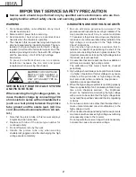
Page 2: ... power receptacle when servicing this chassis X RADIATION AND HIGH VOLTAGE LIMITS 1 Be sure all service personnel are aware of the procedures and instructions covering X radiation The only potential source of X ray in current solid state TV receivers is the picture tube However the picture tube does not emit measurable X Ray radiation if the high voltage is as specified in the High Voltage Check i...

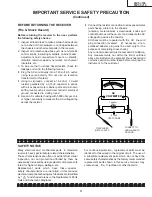
Page 3: ...l parts in the receiver 2 Inspect all protective devices such as non metallic control knobs insulating materials cabinet backs adjustment and compartment covers or shields isolation resistor capacity networks mechanical insulators etc 3 To be sure that no shock hazard exists check for leakage current in the following manner Plug the AC cord directly into a 120 volt AC outlet using reverse polarity...

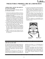
Page 4: ...tre que celui spécifié et ne pas effectuer de modifications déconseillées du circuit à haute tension 6 Lors de la recherche des pannes et des mesures d essai sur un récepteur qui présente une haute tension excessive éviter de s approcher inutilement du récepteur Ne pas faire fonctionner le récepteur plus longtemps que nécessaire pour localiser la cause de la tension excessive AVERTISSEMENT 1 N ent...

Page 5: ...nt étalonnées pour haute tension puissance etc Les pièces de remplacement qui présentent ces caractéristiques sont identifiées dans ce manuel les pièces électriques qui présentent ces particularités sont PRECAUTIONS A PRENDRE LORS DE LA REPARATION Suite 1 Inspecter tous les faisceaux de câbles pour s assurer que les fils ne soient pas pincés ou qu un outil ne soit pas placé entre le châssis et les...

Page 6: ...balanced TUNING RANGES VHF Channels 2 thru 13 UHF Channels 14 thru 69 CATV Channels 1 14 thru 125 EIA Channel Plan VCR SECTION Format VHS Standard Video Recording System Rotary Two Head Helical Scanning Number of Video Heads 2 pcs Video Signal Standard NTSC Color System Tape Width 12 7mm 1 2inch Tape Speed SP 33 35mm sec 1 31i p s LP 16 67mm sec 0 66i p s Play back only EP 11 12mm sec 0 44i p s Ma...

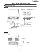
Page 7: ...25VT J100 25VT CJ10 7 LOCATION OF USER S CONTROL Description Of Controls FRONT REAR ...

Page 8: ...25VT J100 25VT CJ10 8 Location Of Control s Buttons Remote Control LOCATION OF USER SCONTROL Continued ...

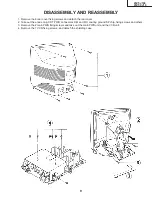
Page 9: ...cover 2 Take out the anode cap CRT PWB connectors K M and RC coating ground SP chip fixing screws and others 3 Remove the 2 main PWB fixing screws and take out the main PWB unit and the VCR unit 4 Remove the 7 VCR fixing screws and detach the shielding case DISASSEMBLY AND REASSEMBLY ...

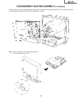
Page 10: ...using control fixing screws and detach the cassette housing control 6 Remove the 4 mechanism chassis fixing screws and detach the mechanism chassis PWB 7 Remove the 8 main PWB fixing screws and detach the main PWB DISASSEMBLY AND REASSEMBLY Continued ...

Page 11: ... servicing any of the components inside disconnect the lead dressing holder Position the main PWB unit upright as shown below and connect the leads for starting the services Note Fit the VCR unit into the front cabinet with the front flap door tilted at 70 80 70 80 ...

Page 12: ...4 Apply external 13 3V DC at TP653 by using an external DC supply The increased voltage will cause the horizontal oscillator to stop and the TV to shut off 5 To re start the osillator remove the external DC power supply and short together TP651 and TP652 Once the TV set operates normally again remove the short between TP651 and TP652 HIGH VOLTAGE CHECK High voltage is not adjustable but must be ch...

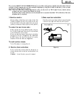
Page 13: ...use the reset function in the video adjust menu to ensure customer controls are in their proper reset position To enter the service mode While pressing the Ch up S2507 button Plug the AC cord into a wall socket Now the TV set is switched on and enters the service mode When successfully entered the service mode will be displayed as shown in Figure A The SERVICE MODE figure the top line stands for s...

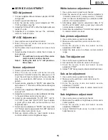
Page 14: ...ube only PICTURE 16 0 63 TINT 33 0 77 COLOR 25 0 63 BRIGHT 28 0 63 SHARP 7 0 13 V PHASE 3 0 7 H PHASE 20 0 31 RF AGC 31 0 63 V AMP 18 0 63 PIF VCO 64 0 127 R CUT OFF 0 0 255 G CUT OFF 0 0 255 B CUT OFF 0 0 255 G GAIN 128 0 255 B GAIN 128 0 255 MUTE 0 0 2 0 Normal raster 1 no 2 No Vertical BALANCE 32 0 63 TEXT POSITION 28 0 128 TEXT PICTURE 20 0 1 CCD LEVEL 7 0 10 OPTION 1 0 3 DATA INTIAL VALUE RAN...

Page 15: ...rightness level SERVICE ADJUSTMENT VCO Adjustment 1 Connect a digital voltmeter between pin 44 of IC401 and ground 2 Select a good local channel 3 Enter the service mode select adjustment PIF VCO and data value 64 4 Adjust the VCO coil T201 so that the digital voltmeter reads 2 5 volts 5 Adjustment is complete remove the voltmeter return to normal mode RF AGC Adjustment 1 Have unit receive a good ...

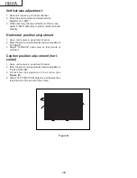
Page 16: ...ion adjustment 1 Have unit receive a good local channel 2 Enter the service mode and select service adjustment H PHASE 3 Adjust H PHASE data value so that picture is centered Caption position adjustment hori zontal 1 Have unit receive a good local channel 2 Enter the service mode and select service adjustment TEXT POSITION 3 A black text box appears on the screen see Figure B 4 Adjust TEXT POSITIO...

Page 17: ...een 2 and 3 of IC701 Check D701 thru D704 L701 R701 and F701 Is AC cord connected Is 170V DC applied to C705 Check T701 and adjacent parts Is 16V DC applied to pin 4 of IC701 Check R708 and IC701 Check IC701 and adjacent parts CRT connector GC1 GC5 bias check The Fuse is again blown out D701 D702 D703 D704 D705 Connect AC cord F701 Check Normal Normal IC701 Check Normal Abnomal IC401 iX2933CE Norm...

Page 18: ...k the IC401 and adjacent parts Check IC2001 Check the Tuner AGC Check the IC351 Does the noise level increase at max Contrast Brightness and Sound Control Is there a signal at pin 43 of IC401 noise increases but no signal is received Is there a signal at pin 41 of IC401 Picture noise decrease but sound level varies greatly Check the tuner bias Normal Abnormal Abnormal Check the IC401 Normal Check ...

Page 19: ...Replace the infrared remote control as required Check pin 10 of IC2001 and or receiver Reposition the set not to be exposed to strong light Is L pulse given out of pin 1 of the receiver and received at pin 4 of IC2001 when the infrared remote control is activated No operation is possible from the infrared remote control Does waveform appear at pin 8 of IC351 Check IC351 and adjacent parts Check IC...

Page 20: ...25VT J100 25VT CJ10 20 H G F E D C B A 1 2 3 4 5 6 CHASSIS LAYOUT PWB F SENSOR UNIT PWB E POWER SW UNIT PWB D VCR KEY UNIT PWB B CRT UNIT PWB C SUB POWER UNIT 25VT CJ100 ONLY ...

Page 21: ...25VT J100 25VT CJ10 21 H G F E D C B A 1 2 3 4 5 6 PWB A MAIN UNIT MODEL 25VT J100 ...

Page 22: ...25VT J100 25VT CJ10 22 H G F E D C B A 1 2 3 4 5 6 PWB A MAIN UNIT MODEL 25VT CJ10 ...

Page 23: ...H G F E D C B A 1 2 3 4 5 6 7 8 9 10 11 12 25VT J100 25VT CJ10 25VT J100 25VT CJ10 23 24 MODEL 25VT J100 BLOCK DIAGRAM OF TV SECTION ...

Page 24: ...H G F E D C B A 1 2 3 4 5 6 7 8 9 10 11 12 25VT J100 25VT CJ10 25VT J100 25VT CJ10 MODEL 25VT CJ10 BLOCK DIAGRAM OF TV SECTION 25 26 ...

Page 25: ...H G F E D C B A 1 2 3 4 5 6 7 8 9 10 11 12 25VT J100 25VT CJ10 25VT J100 25VT CJ10 MODEL 25VT J100 OVERALL SCHEMATIC DIAGRAM 27 28 ...

Page 26: ...H G F E D C B A 1 2 3 4 5 6 7 8 9 10 11 12 25VT J100 25VT CJ10 25VT J100 25VT CJ10 MODEL 25VT CJ10 OVERALL SCHEMATIC DIAGRAM 29 30 ...

Page 27: ...se indicated 2 All voltages measured with 1000µV B W or Color signal DESCRIPTION OF SCHEMATIC DIAGRAM å AND SHADED COMPONENTS SAFETY RELATED PARTS ç MARK X RAY RELATED PARTS DRGANNES MARQUES ET HACHRES PIECES RELATIVES A LA SECURITE MARQUE ç PIECS RELATIVE AUX RAYONS X This circuit diagram is a standard one printed circuits may be subject to change for product improvement without prior notice WAVE...

Page 28: ...H G F E D C B A 1 2 3 4 5 6 7 8 9 10 11 12 25VT J100 25VT CJ10 25VT J100 25VT CJ10 MODEL 25VT J100 SCHEMATIC DIAGRAM MAIN Unit TV Section 33 34 ...

Page 29: ...H G F E D C B A 1 2 3 4 5 6 7 8 9 10 11 12 25VT J100 25VT CJ10 25VT J100 25VT CJ10 35 36 ...

Page 30: ...H G F E D C B A 1 2 3 4 5 6 7 8 9 10 11 12 25VT J100 25VT CJ10 25VT J100 25VT CJ10 MODEL 25VT CJ10 SCHEMATIC DIAGRAM MAIN Unit TV Section 37 38 ...

Page 31: ...H G F E D C B A 1 2 3 4 5 6 7 8 9 10 11 12 25VT J100 25VT CJ10 25VT J100 25VT CJ10 40 39 ...

Page 32: ...H G F E D C B A 1 2 3 4 5 6 7 8 9 10 11 12 25VT J100 25VT CJ10 25VT J100 25VT CJ10 SCHEMATIC DIAGRAM MAIN SENSOR Unit VCR Section 41 SENSOR DUNTK9282WEV0 25VT J100 DUNTK9282WEV3 25VT CJ10 å 42 ...

Page 33: ...H G F E D C B A 1 2 3 4 5 6 7 8 9 10 11 12 25VT J100 25VT CJ10 25VT J100 25VT CJ10 SCHEMATIC DIAGRAM MAIN Unit VCR Section DUNTK9282WEV0 25VT J100 DUNTK9282WEV3 25VT CJ10 43 44 ...

Page 34: ...H G F E D C B A 1 2 3 4 5 6 7 8 9 10 11 12 25VT J100 25VT CJ10 25VT J100 25VT CJ10 PRINTED WIRING BOARD ASSEMBLIES PWB A MAIN Unit Wiring Side 45 46 ...

Page 35: ...H G F E D C B A 1 2 3 4 5 6 7 8 9 10 11 12 25VT J100 25VT CJ10 25VT J100 25VT CJ10 PWB A MAIN Unit Chip Parts Side 47 48 ...

Page 36: ...8 9 10 11 12 25VT J100 25VT CJ10 25VT J100 25VT CJ10 PWB B CRT Unit Wiring Side PWB D VCR KEY Unit Wiring Side Side PWB E POWER SW Unit Wiring Side PWB F SENSOR Unit Wiring Side PWB C SUB POWER Unit Wiring Side 25VT CJ10 ONLY 49 50 ...

Page 37: ...Free 1 800 BE SHARP LISTE DES PIECES CHANGE DES PIECES Les pi eces de rechange qui pr élelesentent ces caract éleristiques sp éleciales de s élecurit éle sont identifi élees dans ce manuel les pi eces élelectriques qui pr élesentent ces particularit éles sont rep éler élee par la marque å et sont hachur élees dans les listes de pi eces et dans les diagrammes sch élematiques La substitution d une p...

Page 38: ... IF Coil AD L303 VP MK220K0000 J Peaking 22µH AB L321 VP XF560K0000 J Peaking 56µH AB Q451 VS2SA1037KQ 1 J 2SA1037 AA Q601 VS2SC2482 1 J 2SC2482 AD å Q612 VS2SD2095 1E J 2SD2095 AN Q735 VS2SC3198 Y 1 J 2SC3198 Y AA Q736 VS2SA1266 Y 1 J 2SA1266 Y AA Q756 VS2SD471 KL1E J 2SD471 AC Q2002 VS2SC2412KQ 1 J 2SC2412 AA Q2201 VS2SC2412KQ 1 J 2SC2412 AA Q2202 VSDTA144EK 1 J DTA144 AC Q2203 VSDTC144EK 1 J DT...

Page 39: ...AA C210 VCKYCY1CF104Z J 0 1 16V Ceramic AA C211 VCCCCY1HH270J J 27p 50V Ceramic AA C241 VCEAGA1CW337MJ 330 16V EL AC C301 VCCCCY1HH470J J 47p 50V Ceramic AA C302 VCCCCY1HH151J J 150p 50V Ceramic AA C303 VCQYTA1HM472K J 4700p 50V Mylar AB C304 VCEAKA1HW105M J 1 50V EL AB C305 VCKYCY1CB104K J 0 1 16V Ceramic AB C306 VCCCCY1HH470J J 47p 50V Ceramic AA C307 VCCCCY1HH101J J 100p 50V Ceramic AA C308 VCK...

Page 40: ...C2202 VCKYCY1HF103Z J 0 01 50V Ceramic AA C2203 VCKYCY1HF103Z J 0 01 50V Ceramic AA C2204 VCKYCY1CF104Z J 0 1 16V Ceramic AA C2205 VCEAKA0JW476M J 47 6 3V EL AB C2207 VCKYCY1CF104Z J 0 1 16V Ceramic AA C2208 VCEAKA1HW225M J 2 2 50V EL AB C2209 VCEAKA1CW106M J 10 16V EL AB C2210 VCEAKA1CW106M J 10 16V EL AB C2211 VCKYCY1HF103Z J 0 01 50V Ceramic AA C2212 VCKYCY1CF104Z J 0 1 16V Ceramic AA C2213 VCK...

Page 41: ... 50V Mylar AB C6627 VCKYCY1EB183K J 0 018 25V Ceramic AA C6628 VCKYCY1HB682K J 6800p 50V Ceramic AA C7701 VCKYCY1HF103Z J 0 01 50V Ceramic AA C7702 VCKYCY1HF103Z J 0 01 50V Ceramic AA C7704 VCKYCY1CF104Z J 0 1 16V Ceramic AA C7705 VCCCCY1HH220J J 22p 50V Ceramic AA C7706 VCCCCY1HH220J J 22p 50V Ceramic AA C7707 VCKYCY1HF103Z J 0 01 50V Ceramic AA C7708 VCKYCY1HB272K J 2700p 50V Ceramic AA C7709 VC...

Page 42: ... VRD RA2BE471J J 470 1 8W Carbon AA R505 VRD RA2BE101J J 100 1 8W Carbon AA R506 VRD RA2BE124G J 120k 1 8W Carbon AA R507 VRD RA2BE104G J 100k 1 8W Carbon AA R508 VRD RA2BE473J J 47k 1 8W Carbon AA R510 VRN VV3AB1R0J J 1 1W Metal Film AA å R511 VRN SV2HB1R0J J 1 1 2W Metal Film AA R512 VRS VV3AB391J J 390 1W M Ox AA R513 VRD RA2BE182J J 1 8k 1 8W Carbon AA R516 VRD RA2BE332J J 3 3k 1 8W Carbon AA ...

Page 43: ...k 1 16W M Ox AA R2240 VRS CY1JF223J J 22k 1 16W M Ox AA R2241 VRS CY1JF183J J 18k 1 16W M Ox AA R2244 VRS CY1JF562J J 5 6k 1 16W M Ox AA R2247 VRS CY1JF561J J 560 1 16W M Ox AA R2248 VRS CY1JF272J J 2 7k 1 16W M Ox AA R2249 VRS CY1JF681J J 680 1 16W M Ox AA R2250 VRS CY1JF471J J 470 1 16W M Ox AA R2251 VRS CY1JF102J J 1k 1 16W M Ox AA R2252 VRS CY1JF272J J 2 7k 1 16W M Ox AA R2253 VRS CY1JF104J J ...

Page 44: ...32 VRS CY1JF223J J 22k 1 16W M Ox AA R7701 VRS CY1JF102J J 1k 1 16W M Ox AA R7702 VRS CY1JF102J J 1k 1 16W M Ox AA R7703 VRD RA2BE102J J 1k 1 8W Carbon AA R7707 VRD RA2BE102J J 1k 1 8W Carbon AA R7708 VRD RA2BE102J J 1k 1 8W Carbon AA R7711 VRS CY1JF102J J 1k 1 16W M Ox AA R7712 VRS CY1JF102J J 1k 1 16W M Ox AA R7719 VRD RA2BE102J J 1k 1 8W Carbon AA R7720 VRD RA2BE102J J 1k 1 8W Carbon AA R7724 V...

Page 45: ...7803 VRS CY1JF103J J 10k 1 16W M Ox AA R7804 VRD RA2BE222J J 2 2k 1 8W Carbon AA R7805 VRS CY1JF103J J 10k 1 16W M Ox AA R7806 VRS CY1JF103J J 10k 1 16W M Ox AA å R7807 VRG SC2EB1R8J J 1 8 1 4W M Ox AE R7808 VRD RA2BE102J J 1k 1 8W Carbon AA R7809 VRS CY1JF822J J 8 2k 1 16W M Ox AA R7810 VRS CY1JF822J J 8 2k 1 16W M Ox AA R7811 VRS CY1JF822J J 8 2k 1 16W M Ox AA R7812 VRS CY1JF822J J 8 2k 1 16W M ...

Page 46: ...Carbon AA R858 VRD RA2BE181J J 180 1 8W Carbon AA å R859 VRS VV3LB123J J 12k 3 0W M Ox AB å R861 VRS VV3LB123J J 12k 3 0W M Ox AB å R863 VRS VV3LB123J J 12k 3 0W M Ox AB R876 VRD RA2BE121J J 120 1 8W Carbon AA R877 VRD RA2BE121J J 120 1 8W Carbon AA R878 VRD RA2BE121J J 120 1 8W Carbon AA R880 VRD RM2HD222J J 2 2k 1 2W Carbon AA R881 VRD RM2HD222J J 2 2k 1 2W Carbon AA R882 VRD RM2HD222J J 2 2k 1 ...

Page 47: ...501 QPLGN0278GEZZ J Plug 2 pin RC AA QCNW 1942PEZZ J Connecting Cord AE PWB D DUNTK9056WEV8 VCR KEY UNIT PWB F DUNTK9066WEV0 SENSOR UNIT DIODES D7702 RH PX0252GEZZ J GP1S563 AF D7703 RH PX0252GEZZ J GP1S563 AF D7704 RH PX0253GEZZ J GP1S94 AF D7705 RH PX0253GEZZ J GP1S94 AF D7707 RH PX0234GEZZ J LED AD CAPACITORS C7722 VCKYD41CY103N J 0 01 16V Ceramic AA C7723 VCKYD41CY103N J 0 01 16V Ceramic AA C7...

Page 48: ...AJFJ V Pinch Double Action AD Spring 33 MSPRT0405AJFJ V Tension Spring AE 34 NBLTK0067AJ00 V Drive Belt AE 35 NDAiV1070AJ00 V Reel Disk AE 36 NGERH1267AJZZ V Loading Connect Gear AD 37 NGERH1268AJ00 V Master Cam AE 38 NGERH1269AJZZ V Casecon Drive Gear AD 39 NGERH1270AJZZ V Take Up Loading Gear AF 40 NGERH1271AJZZ V SupplyLoading Gear AD 41 NGERH1272AJZZ V Pinch Drive Cam AE 42 NGERH1289AJZZ V Sup...

Page 49: ...SM CHASSIS PARTS 66 62 62 66 63 67 53 66 64 65 26 57 55 201 56 59 28 28 202 202 16 200 207 207 49 7 218 8 200 49 11 216 203 5 41 61 3 17 216 38 21 208 37 9 30 36 39 216 45 48 27 40 30 10 23 43 216 217 35 46 42 35 215 209 210 211 212 213 4 52 2 58 206 15 33 1 50 34 54 60 47 51 44 6 205 204 24 25 22 12 31 214 19 68 29 18 20 ...

Page 50: ... 7 AD 214 PSPAP0009AJZZ V Reverse Guide AB Adjusting Nut 215 LX WZ1003GE00 J Cut Washer AA 216 LX WZ1041GE00 J Cut Washer AA 217 LX WZ1073GE00 J Cut Washer AB 218 XBPSD30P08J00 J Drum Base Mounting AA Screw SW3P 8S 300 CHLDX3074TEV0 V Cassette Housing AX Control Ass y 301 LANGF9592AJFW V Upper Plate AL 302 LHLDX1028AJ00 V Frame L AH 303 LHLDX1029AJ00 V Frame R AH 304 LHLDX1030AJZZ V Holder L AE 30...

Page 51: ...t No Description Code Ref No Part No Description Code 25VT J100 25VT CJ10 65 H G F E D C B A 1 2 3 4 5 6 CASSETTE HOUSING CONTROL PARTS 304 301 311 311 305 308 302 313 306 309 303 310 317 314 312 307 315 316 300 ...

Page 52: ...11 XTASD30P12000 J Screw AA 12 LX TZ3011CEFD J Screw AA 13 VSP0080PBK98A J Speaker AP 14 XTASD40P16000 J Screw AA 15 GCABB1114MEKA M Cabinet Rear BB 16 XTASD40P20000 J Screw x6 AA 17 LHLDZ0094PEZZ R Sensor Holder AC 18 LX HZ3001PEFD R Screw AA 19 XHPSD30P06WS0 J Screw AA 20 LCHSM0056PEKZ R Chassis Frame AW 21 PSLDM0215PEFW R Shield Case Top AQ 22 PSLDM0202PEFW R Shield Case Bottom AK 23 PSLDM0205P...

Page 53: ...H G F E D C B A 1 2 3 4 5 6 7 8 9 10 11 12 25VT J100 25VT CJ10 25VT J100 25VT CJ10 CABINET AND MECHANICAL PARTS 67 68 ...

Page 54: ...Guarantee Card AA 25VT J100 TiNS 6068MEZZ M Operation Manual AF 25VT J100 TCAU3025MEZZ M Safety Tip AA 25VT J100 TiNS 6132MEZZ M Operation Manual 25VT CJ10 Ref No Part No Description Code Ref No Part No Description Code PACKING OF THE SET SETTING POSITIONS OF THE KNOBS Power SW OFF Channel 2ch S Volume About 20 50 REAR Use tapes to fix the packing case Packing case FRONT Buffer material Polystyren...

Page 55: ...25VT J100 25VT CJ10 71 Memo ...

Page 56: ...25VT J100 25VT CJ10 72 TQ0276 S YO KG Printed in U S A ...

Reviews: