background image

3

21HS-50H

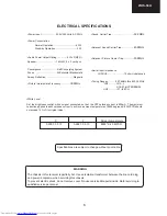
ELECTRICAL SPECIFICATIONS

Power Input .......................220V-240 Volts AC 50Hz

Power Consumption

Audio Power Output Rating ................4W x 2(MPO)

Speaker................................16

 4W, 9 x 5 cm,2pcs

Normal Operation....................................43W

Stand-by Operation...................................3W

White Level

Set  the brightness control, with no signal connected, so that  the CRT cathode current is 600mA.  The maximum
correction applied to each cathode current to achieve a screen temperature of 8900 degrees K-20 MPCD should
not exceed 15% of its original value.

Convergence.........................Self Converging System

Focus....................................Bi-Potencial Electrostatic

Sweep Deflection...........................................Magnetic

Aerial Input Impedance

VHF/UHF..........................75 ohm Unbalanced

Tuning Ranges ............45.75MHz thru 855.25 MHz

         VHF.............IR A - J

                                        S1-S41 (HYPERBAND)
                    UHF.............I21 - I69 CH

Picture Intermediate Frecuency.....

.........38.9MHz

Sound  Carrier Trap

...............................32.9MHz

Adjacent  Sound Carrier Trap

.................40.9MHz

Adjacent  Picture  Carrier Trap

...............30.9MHz

                                            WARNING

The chassis in this receiver is partially hot. Use an isolation transformer between the line cord plug
and power receptacle, when servicing this chassis.
To prevent electric shock, do not remove cover. No user-serviceable parts inside. Refer servicing to
qualified service personnel.

Specifications are subject to change without prior notice.

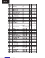
X

Y

Screen temperature

0.290 

±

 0.015

0.284 

±

 0.015

8900º K-20 MPCD

Summary of Contents for 21HS-50H

Page 1: ...to its original condition and only parts identical to those specified should be used This document has been published to be used for after sales service only ELECTRICAL SPECIFICATION 3 IMPORTANT SERVICING NOTES 4 CONTROLS TERMINALS 5 SERVICE ADJUSTMENTS 6 CHASSIS LAYOUT 12 LED FLASHING CODE 13 PRINTED WIRING BOARDS 13 ICs ADDITIONAL INFORMATION 18 SCHEMATIC DIAGRAM WAVE FORMS 26 BLOCK DIAGRAM 32 T...

Page 2: ...f only part number changes are required just change part number directly the part number in the Parts Listing Section If you need more information please refer to the Technical Report Bulletin SERVICE MANUAL UPDATE LOG SHEET Part No Technical Report No Technical Bulletin No Cause Solution Page No Application Data Serial No ...

Page 3: ...Electrostatic Sweep Deflection Magnetic Aerial Input Impedance VHF UHF 75 ohm Unbalanced Tuning Ranges 45 75MHz thru 855 25 MHz VHF IR A J S1 S41 HYPERBAND UHF I21 I69 CH Picture Intermediate Frecuency 38 9MHz Sound Carrier Trap 32 9MHz Adjacent Sound Carrier Trap 40 9MHz Adjacent Picture Carrier Trap 30 9MHz WARNING The chassis in this receiver is partially hot Use an isolation transformer betwee...

Page 4: ... x ray radiation levels This is a problem when in close proximity to the receiver for long periods of time To reduce any risks associated with this please observe the following precautions 1 When undertaking any servicing on this chassis DO NOT increase the EHT to more than 30 5 KV at a instantaneous beam current of 1300µΑ 2 EnsurethatduringnormaloperationtheEHTdoesnotexceed25 0KV 1 5KV atabeamcur...

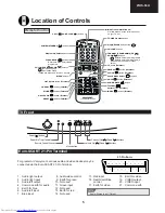
Page 5: ...VEAL button Teletext TV button Teletext HOLD button Teletext CHANNEL PROGRAMME UP DOWN buttons Selects next higher programme Selects next lower programme These are also used for menu set up STORE button Teletext SOUND MUTE button CLOCK button Teletext Sound Mode Select button INDEX button Teletext LIST Select button Teletext 26 Location of Controls Remote Control TV Front Euro SCART 21 Pin Termina...

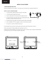
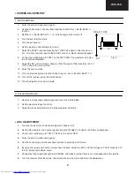
Page 6: ... 5 Keep pressing the volume down and channel up buttons until the picture appears 6 When SHARPX X VXX XX appears on the screen release the two buttons 7 The receiver is now in the service mode See Fig 2 To move between the various service mode functions use the channel up and down buttons See Fig 3 Use the volume buttons to change the data to the desired value See Fig 3 The data will be stored aut...

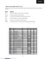
Page 7: ...0 32 16 9 FIX 16 DRI RC White point Red Cold white temp 0 32 16 9 FIX 17 DRI GC White point Green Cold white temp 0 32 16 9 FIX 18 DRI BC White point Blue Cold white temp 0 32 16 16 FIX 19 SUB VOL Max Volume 0 63 60 60 FIX 20 SUB CON Sub Contrast 0 63 63 63 FIX 21 SUB COL Sub Colour 0 63 32 25 FIX 22 SUB BRI Sub Brightness 0 63 32 34 FIX 23 TINT Sub Tint 0 63 32 32 FIX 24 SUB SHP Sub Sharpness 0 6...

Page 8: ... Limit 0 disable or 1 enable 0 1 FIX 53 S L Sound system L 0 disable or 1 enable 0 0 FIX 54 S DK Sound system DK 0 disable or 1 enable 1 0 FIX 55 S I Sound system I 0 disable or 1 enable 1 1 FIX 56 S BG Sound system BG 0 disable or 1 enable 1 0 FIX 57 BLUE BACK Video mute at Ident loss 0 disable or 1 enable 1 1 FIX 58 VMC Video Mute at program source Change 0 disable or 1 enable 1 1 FIX 59 HTL Hot...

Page 9: ...UUE BACK 1 12 Turn off the receiver using the mains button 13 The G2 adjustment is now complete 2 Focus Adjustment 1 Receive a monoscope pattern signal at a level of 60 to 80 dBuV 2 Set the picture settings to normal 3 Adjust the focus potentiometer to obtain maximum definition AGC ADJUSTMENT 1 Tune the receiver into a colour bar signal on channel E 12 2 Set the RF generator to an output signal st...

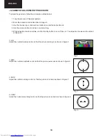
Page 10: ...justments are complete use the standby button to turn off the set The adjustment values will be stored at this point V LIN Adjust the vertical linearity control so that the picture centring is as shown in figure 5 V AMP Adjust the vertical amplitude control so that the picture overscans as shown in figure 6 V CENT Adjust the vertical centring control so that the picture is centred as shown in figu...

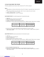
Page 11: ...ions to obtain colour co ordinates 6 Re set the TV with the mains switch button to store the adjustment and exit service mode 7 Check colour co ordinates X and Y at 20 a 120 Nits It may be necessary to repeat the same procedure to obtain the above values ADJUSTMENT METHOD 2 using the signal generator with a fixed picture signal 1 Adjust G2 2 Tune a white pattern with burst signal 3 Operate in serv...

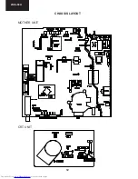
Page 12: ...12 21HS 50H CHASSIS LAYOUT MOTHER UNIT CRT UNIT ...

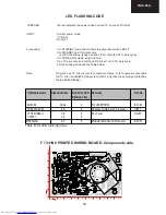
Page 13: ...ing If in STANDBY mode and On timer in active then switch LED off If in STANDBY and On timer active set LED to blinking switch on and off at 1 Hz with a 50 duty cycle If in POWER ON mode switch LED on If an I2 C error occurred let the LED blink at 1 Hz 50 duty cycle For the blinking times see the Table below Note Only when an I2 C error occurs for a number of times or for a number of seconds the I...

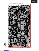
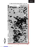
Page 14: ...14 21HS 50H F 7340N4 PRINTED WIRING BOARD Components side Page 15 22 23 24 25 17 18 19 20 21 11 12 13 14 15 16 1 2 3 4 5 6 7 8 9 10 Y X 0 1 10 11 12 13 2 3 4 5 6 7 8 9 ...

Page 15: ...15 21HS 50H F 7340N4 PRINTED WIRING BOARD Components side Page 14 Y X 1 2 3 20 21 22 23 24 25 12 13 14 15 16 17 18 19 22 23 24 25 17 18 19 20 21 11 12 13 14 15 16 4 5 6 7 8 9 10 ...

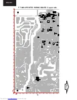
Page 16: ...16 21HS 50H F 7340N4 PRINTED WIRING BOARD Copper side X 22 23 24 25 17 18 19 20 21 11 12 13 14 15 16 1 2 3 4 5 6 7 8 9 10 Y 19 18 17 16 15 14 13 12 25 24 23 22 21 20 Page 17 ...

Page 17: ...17 21HS 50H F 7340N4 PRINTED WIRING BOARD Copper side Y X 22 23 24 25 17 18 19 20 21 11 12 13 14 15 16 1 2 3 4 5 6 7 8 9 10 0 10 9 8 7 6 5 4 3 2 1 13 12 11 Page 16 ...

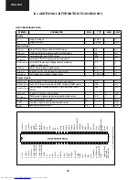
Page 18: ...RAMETER MIN TYP MAX UNIT Supply VP supply voltages 8 0 3 3 V IP supply current 135 60 mA Input voltages ViVIFrms video IF amplifier sensitivity RMS value 75 µV ViSIF rms QSS sound IF amplifier sensitivity RMS value 60 µV ViAUDIO rms external audio input RMS value 500 mV ViCVBS p p external CVBS Y input peak to peak value 1 0 V ViCHROMA p p external chroma input voltage burst amplitude peak to peak...

Page 19: ...SHIFT V DRIVE CONTR BRIGHTN OSD TEXT INSERT CCC WHITE P ADJ 80C51 CPU I 2 C BUS TRANSCEIVER ROM RAM TELETEXT ACQUISITION 1 10 PAGE MEMORY TELETEXT OSD DISPLAY R G B BL Y U V H V REF ENHANCED VST PWM DAC VST OUT I O PORTS I O PORTS 4x 3 3 V RESET LED OUT 2x ADC IN 4x VPE EW GEOMETRY GEOMETRY EHTO EWD R V G Y B U BL RGB YUV INSERT R G B REF CVBS SYNC H V COR 27 37 38 33 20 29 28 34 44 60 55 59 58 57...

Page 20: ...or TV processor DECBG 19 bandgap decoupling AVL EWD 1 20 Automatic Volume Levelling East West drive output VDRB 21 vertical drive B output VDRA 22 vertical drive A output IFIN1 23 IF input 1 IFIN2 24 IF input 2 IREF 25 reference current input VSC 26 vertical sawtooth capacitor TUNERAGC 27 tuner AGC output AUDEEM SIFIN1 1 28 audio deemphasis or SIF input 1 DECSDEM SIFIN2 1 29 decoupling sound demod...

Page 21: ...G input Y input B2 UIN 48 2nd B input U B Y input BCLIN 49 beam current limiter input V guard input note 2 BLKIN 50 black current input V guard input note 2 RO 51 Red output GO 52 Green output BO 53 Blue output VDDA 54 analog supply of Teletext decoder and digital supply of TV processor 3 3 V VPE 55 OTP Programming Voltage VDDC 56 digital supply to core 3 3 V OSCGND 57 oscillator ground supply XTA...

Page 22: ...START UP CURRENT SOURCE 0 75 V 0 5 V 5 Isense 6 DRIVER MGU230 4 DEM 8 DRAIN 7 HVS n c OCP LEB blank Iss 2 5 V burst detect Block diagram PINNING SYMBOL PIN DESCRIPTION VCC 1 supply voltage GND 2 ground CTRL 3 control input DEM 4 input from auxiliary winding for demagnetization timing OVP and OPP Isense 5 programmable current sense input DRIVER 6 gate driver output HVS 7 high voltage safety spacer ...

Page 23: ...GND Input 8 N C 9 Volume Circuit Function Block Diagram Pin Descriptions Note Do not apply voltage or current to NC pin from outside Pin No Pin Name 1 Inverting Input 2 Power Supply 3 Pump up Output 4 GND 5 Vertical Output 6 Vertical Output Power Supply 7 Non inverting Input Pin Descriptions Non inverting Input Output Vcc Output GND Pump Up Out Vcc Inverting Input 1 2 3 4 5 6 7 Pump Up Thermal Pro...

Page 24: ...ly Voltage AVSUP 0 3 6 0 V dVSUP23 Voltage between AVSUP and DVSUP AVSUP DVSUP 0 5 0 5 V PTOT Package Power Dissipation PSDIP64 PSDIP52 PQFP80 PLQFP64 PMQFP44 AHVSUP DVSUP AVSUP 1300 1200 1000 960 960 mW mW mW mW mW VIdig Input Voltage all Digital Inputs 0 3 VSUP2 0 3 V IIdig Input Current all Digital Pins 20 20 mA1 VIana Input Voltage all Analog Inputs SCn_IN_s 2 MONO_IN 0 3 VSUP1 0 3 V IIana Inp...

Page 25: ...REF2 NC NC ANA_IN1 ANA_IN TESTEN XTAL_IN XTAL_OUT AVSUP TP D_CTR_I O1 D_CTR_I O0 ADR_SEL STANDBYQ MSP 34x5G 34 35 36 37 38 39 40 41 42 43 44 22 21 20 19 18 17 16 15 14 13 12 1 2 3 4 5 6 7 8 9 10 11 33 32 31 30 29 28 27 26 25 24 23 Simplified functional block diagram of MSP 34x5G Source Select Loud SCART1 SCART1 SCART2 MONO De modulator speaker Sound Processing DAC ADC Loud DAC ADC Sound IF1 speake...

Page 26: ...NCLOSED BY THIS LINE IS DIRECTLY CONNECTED WITH AC MAINS VOLTAGE WHEN SERVICING THE AREA CONNECT AN ISOLATING TRANSFORMER BETWEEN TV RECEIVER AND AC LINE TO ELIMINATE HAZARD OF ELECTRIC SHOCK CAUTION This circuit diagram is original one therefore there may be slight difference from yours IMPOTANT SAFETY NOTE PARTS MARKED WITH ARE IMPORTANT FOR MAINTAINING THE SAFETY OF THE SET BE SURE TO REPLACE T...

Page 27: ...27 21HS 50H ...

Page 28: ...28 21HS 50H Page 29 1 I H G F E D C B A 2 3 4 5 6 7 SCHEMATIC DIAGRAM OF MOTHER UNIT F7340N4 01 Version ...

Page 29: ...29 21HS 50H SCHEMATIC DIAGRAM OF MOTHER UNIT F7340N4 01 Version 8 9 10 11 12 13 14 I H G F E D C B A Page 28 Page 30 ...

Page 30: ...30 21HS 50H SCHEMATIC DIAGRAM OF MOTHER UNIT F7340N4 01 Version 8 9 10 11 12 13 14 I H G F E D C B A Page 29 ...

Page 31: ...31 21HS 50H SCHEMATIC DIAGRAM OF CRT F7341N0 00 Version 1 I H G F E D C B A 2 3 4 5 6 7 ...

Page 32: ...32 21HS 50H CRT UNIT BLOCK DIAGRAM 1 I H G F E D C B A 2 3 4 5 6 7 ...

Page 33: ...33 21HS 50H MOTHER UNIT BLOCK DIAGRAM 1 I H G F E D C B A 2 3 4 5 6 7 ...

Page 34: ...Main B Abnormal Approx 110V Normal YES Check D758 IC702 IC753 Check CRT connector K1 D1001 Power LED Bright Red and D762 K5 bias turns on NO Normal Normal Abnormal NO D1001 Power LED Dark Red Check R615 Check Check turns on C878 IC801 Checking the D1001 turns on protector circuit brightly and darkly Bus error NVM IC1002 See many often D1001 TV PROCESSOR flashes in red IC801 This indicates which IC...

Page 35: ...ERTICAL SCAN Check IC501 bias Normal Abnormal Check C502 and C514 Check IC501 NO SPECIFIC COLOUR NO YES Is some colour produced in B W broadcast reception Check IC801 R801 R802 YES Is the white balance R803 D804 D805 D806 properly adjusted and Q801 NO Readjusted the white balance The picture colour is cyan The picture colour is magenta The picture colour is yellow Check Q870 Q885 and Check Q871 Q8...

Page 36: ... IC801 circuit NO YES Check the tuner Does noise or AGC at TP201 signal appear at Check Q401 pin23 and 24 Q402 and related Normal Abnormal of IC801 circuit NO YES Check pin38 Check pin27 Check pin1 2 of of IC801 of IC801 Tuner SF201 Tuner Check pin37 of and related circuit and related IC801 and circuit related circuit NO SOUND CIRCUITS TO BE CHECKED NO Audio Output Circuit Does signal appear Check...

Page 37: ...0K0000 PEAK COIL 10UH 10 1 8W S AA AA L 0802 VP XF100K0000 PEAK COIL 10UH 10 1 8W S AA AA L 1002 VP XF100K0000 PEAK COIL 10UH 10 1 8W S AA AA L 3001 VP DF100K0000 PEAK COIL 10UH 10 S AA AA L 3002 VP DF100K0000 PEAK COIL 10UH 10 S AA AA L 3003 VP DF100K0000 PEAK COIL 10UH 10 S AA AA L 3030 VP CF3R3K0000 PEAK COIL 3 3UH 10 S AB AB L 3050 VP CF3R3K0000 PEAK COIL 3 3UH 10 S AB AB L 3060 VP CF3R3K0000 ...

Page 38: ...AA C 0532 VCKYCY1HB102K S CHIP CAP 0 001UF 50V S AA AA C 0533 VCQYTA1HM104J F CAPACITOR 0 1 UF 50 V S AA AB C 0599 VCKYPA1HB102K C CAPACITOR 1000PF 50V S AA AA C 0602 VCEA0A1CW477M ELEC C 470UF 20 16V S AA AB C 0603 VCEA0A1CW107M ELEC C 100UF 20 16V S AA AA C 0604 VCKYPA1HF103Z C CAPACITOR 0 01U F 50V S AA AA C 0605 VCEA0A1AW227M ELEC C 220UF 20 10V S C 0606 VCEA0A1CW107M ELEC C 100UF 20 16V S AA ...

Page 39: ... TAPED S AA AA R 0453 VRS CY1JF223J S CHOP REG 22K OHM T S AA AA R 0454 VRS CY1JF562J S CHIP RES 5 6K OHM TAPED S AA AA REF No PARTS DESCRIPTION SN CODE EX CODE R 0455 VRD RA2EE750J RES 75 OHM 5 1 4W S AA AA R 0456 VRD RA2EE750J RES 75 OHM 5 1 4W S AA AA R 0457 VRD RA2EE750J RES 75 OHM 5 1 4W S AA AA R 0458 VRS CY1JF103J S C RESISTOR 10K OHM S AA AA R 0459 VRD RA2EE750J RES 75 OHM 5 1 4W S AA AA R...

Page 40: ...ES 33K OHM TAPED S AA AA R 3012 VRS CY1JF103J S C RESISTOR 10K OHM S AA AA RJ 0001 VRS CY1JF000J S CHIP RES 0 OHM TAPED S AA AA RJ 0002 VRS CY1JF000J S CHIP RES 0 OHM TAPED S AA AA RJ 0004 VRS CY1JF000J S CHIP RES 0 OHM TAPED S AA AA REF No PARTS DESCRIPTION SN CODE EX CODE RJ 0008 VRS CY1JF000J S CHIP RES 0 OHM TAPED S AA AA RJ 0009 VRS CY1JF000J S CHIP RES 0 OHM TAPED S AA AA RJ 0010 VRS CY1JF00...

Page 41: ...VRS VV3DB153J MET OX RES 15KOHM 5 2W S AA AA R 0887 VRD RA2HD272J RES 2 7KOHM 5 1 2W S AA AA R 0892 VRD RA2BE102J RES 1KOHM 5 1 8W S AA AA R 0893 VRD RA2BE102J RES 1KOHM 5 1 8W S AA AA R 0894 VRD RA2BE102J RES 1KOHM 5 1 8W S AA AA R 0895 VRD RA2BE471J RES 470 OHM 5 1 8W S AA AA R 0896 VRD RA2BE471J RES 470 OHM 5 1 8W S AA AA R 0899 VRD RA2BE471J RES 470 OHM 5 1 8W S AA AA MISCELLANEOUS PARTS P 085...

Page 42: ... GreenChipII SMPS controlIC Preliminary specification 2000Dec05 3 AN7523 Matsushita Electronics Corporation Specifications AN7523 Product Specifications Doc No SDSC PSE AN7503 Eff Date 23 FEB 01 4 AN5522 Matsushita Electronics Corporation Specifications AN5522 Product Specifications Doc No SDSC PSE AN5522 Eff Date 21 NOV 2000 5 MSP34x5G Micronas Preliminary Data sheet MSP34x5g Multistandard Sound ...

Page 43: ...43 21HS 50H NOTES ...

Page 44: ...itted in any form or by any means electronic mechanical photocopying recording or otherwise without prior written permission of the publisher SHARP ELECTRONICA ESPAÑA S A TV Division Engineering Dept Polígono Industrial Can Sant Joan Sant Cugat del Vallès Barcelona Spain Think Ecology please use RECYCLED PAPER ...

Reviews: