25
CABINET AND CHASSIS PARTS 1
SX81R/J Parts List1
CABINET 1
1
2
3
4
5
6
7
8
9
10
11
12
13
14
15
16
17
18
19
20
21
22
23
24
26
27
101
103
104
105
102
Page 1: ...e wattage and voltage ratings shown CAUTION Danger of explosion if battery is incorrectly replaced Replace only with the same or equivalent type recommended by the manufacturer Discard used batteries according to the manufacturer s instructions NOTE 1 Parts order must contain model number part number and description 2 Substitute parts may be supplied as the service parts 3 N S P Not available as s...
Page 2: ...alent and which lets you adjust the tip temperature up to 450 C 842 F It should also have as good temperature recovery characteris tics as possible Set the temperature to 350 C 662 F or less for chip compo nents to 380 C 716 F for lead wires and similar and to 420 C 788 F when installing and removing shield plates The tip of the soldering iron should have a C cut shape or a driver shape so that it...
Page 3: ... G G B G B 13 14 16 V DD 15 V OUT V Ø7B V Ø8 Note Note Photo sensor Horizontal register Vertical register Pin No 1 Symbol 2 3 4 5 6 7 8 9 10 Vø1A Vø1B Vø2 Vø3A Vø3B VøST Vø4 Vø5B VøHLD Pin Description Vertical register transfer clock Vertical register transfer clock Vertical register transfer clock Horizontal addition control clock Vertical register transfer clock Vertical register transfer clock ...
Page 4: ...put to pins 27 of IC905 There are S H blocks inside IC905 gener ated from the XSHP and XSHD pulses and it is here that CDS correlated double sampling is carried out After passing through the CDS circuit the signal passes through the AGC amplifier It is A C converted internally into a 12 bit signal and is then input to IC101 of the CP1 circuit board The gain of the AGC amplifier is controlled by pi...
Page 5: ...gnals take a picture commands from the 8 bit microprocessor is input to ASIC IC101 and operation starts When the TG SG drives the CCD picture data passes through the A D and CDS and is then input to the ASIC as 12 bit data The AF AE AWB shutter and AGC value are computed from this data and three expo sures are made to obtain the optimum picture The data which has already been stored in the SDRAM i...
Page 6: ...gnals FIN1 FIN2 FIN3 and FIN4 which are output from the ASIC IC101 are used to drive AFSPM 1 A AFSPM 2 A AFSPM 3 B and AFSPM 4 B by the motor driver IC951 Detection of the standard focusing positions is carried out by means of the photointerruptor AFPI inside the lens block 4 4 Zoom drive The zoom DC motor drive signals ZIN1 and ZIN2 which are output from the ASIC IC101 are used to drive ZM and ZM...
Page 7: ...sor is driven 2 1 Damage Prevention Circuit When a short circuit is generated for a constant period of time the capacitor that is connected to pin 1 of IC501 turns all output off It is also equipped with an overheating protection circuit so that when the element temperature becomes higher than a certain temperature all output is turned off in the same way as for a short circuit To reset output rem...
Page 8: ...Rectifier circuit The high voltage alternating current which is generated at the secondary side of T5401 is rectified to produce a high voltage direct current and is accumulated at electrolytic ca pacitor C5412 on the main circuit board 1 6 Voltage monitoring circuit This circuit is used to maintain the voltage accumulated at C5412 at a constance level After the charging voltage is divided and con...
Page 9: ... O O I I O O O Outline Battery OFF detection SW 3 2 V line ON Always low output Lens power PFM PWM mode switching L PFM H PWM Microprocessor reset terminal Clock oscillation terminal for clock Clock oscillation terminal for clock Program writing control signal mode lead in Main clock oscillation terminal 4 MHz Regulator output for internal operation GND GND Power terminal Power terminal System res...
Page 10: ... and ASIC 8 bit micro processor ASIC MRST PLLEN SI SO SCK SREQ communi cation COMREQ setting of external port 45 NOT USED 46 NOT USED 47 AVREF I Internal A D standard potential 48 AVSS Analog GND A D GND 49 BATTERY I Battery potential detection A D 50 VMONIT I Strobo condensor charge potential detection A D 51 ILLUMI I Illuminance sensor potential detection A D 52 TOUCH_IN I Touch sensor input A D...
Page 11: ...ounting by subclock Also the battery for backup is charged 10 hours from it to be attached When the power switch is on the 8 bit microprocessor starts processing The 8 bit microprocessor first sets both the PON signal at pin 30 and the PAON signal ASIC to High and then turn on the power circuit After PON signal is to High sets external port of ASIC after approximately 100 ms According to setting o...
Page 12: ... 3 5 2 Three screws 1 7 x 4 3 Two screws 1 7 x 3 4 Cabi back 5 Holder battery 6 Shaft zoom 7 LCD 8 FPC 9 Remove the solder 10 Two screws 1 4 x 3 5 11 Cabi front NOTE Discharge a strobe capacitor with the discharge jig VJ8 0188 for electric shock prevention 1 2 3 4 5 6 7 8 9 10 11 2 ...
Page 13: ... Two screws 1 4 x 3 6 Two screws 1 4 x 3 7 Holder monitor 8 Earth dec lens 9 Screw 1 4 x 3 10 Earth switch back 11 Spacer CP1 12 Speaker 8 13 Remove the solder 14 Screw 1 4 x 3 15 Screw 1 4 x 3 16 Stand 17 Remove the solder 18 Microphone 19 Spacer lens top 1 2 3 4 5 6 7 8 9 10 11 12 13 14 15 16 17 18 19 ...
Page 14: ...e solder 6 Remove the solder 7 Three screws 1 4 x 3 8 Remove the solder 9 Assy lump When assembling tighten the screws order a b c 1 2 3 4 5 6 7 8 9 10 11 12 13 14 15 16 17 18 a b c 10 Condensor 11 Two screws 1 7 x 2 5 12 Terminal battery B 13 Terminal battery A 14 Holder battery 15 Three screws 1 4 x 3 5 16 FPC 17 Lens assembly 18 CP1 board ...
Page 15: ... 15 2 4 BOARD LOCATION TB1 board CP1 board ...
Page 16: ...older on the hard disk 3 Installing USB driver Install the USB driver with camera or connection kit for PC 4 Pattern box color viewer Turn on the switch and wait for 30 minutes for aging to take place before using Color Pure It is used after adjusting the chroma meter VJ8 0192 adjust color temperature to 3100 20 K and luminosity to 900 20 cd m2 Be careful of handling the lump and its circumference...
Page 17: ... 1 Line up the arrow on the cable connector with the notch on the camera s USB port Insert the connector 2 Locate a USB port on your computer 3 Insert the AC adaptor s cable to DC adaptor cable Insert the DC adaptor to the camera 4 If USB CONNECTION is displayed choose the CARD READER and press the SET button AC adaptor To USB port USB cable ...
Page 18: ...45 112 AF_MID2 focus adjustment vallue M2 45 112 AF_MID3 focus adjustment vallue M3 45 112 AF_MID4 focus adjustment vallue M4 45 112 AF_TELE focus adjustment vallue T 26 112 Camera Collimator COMPL PWB CP 1 636 095 5288 Lens Adjustment AWB Adjustment CCD White Point Defect Detect Adjustment CCD Black Point And White Point Defect Detect Adjustment In Lighted Factory Cord Setting USB storage informa...
Page 19: ...600 Adjustment values other than the above are irrelevant 3 CCD White Point Defect Detect Adjustment Adjustment method 1 Double click on the DscCalDi exe 2 Select CCD Defect on the LCD Test and click the Yes 3 After the adjustment is completed OK will display 4 Click the OK 4 CCD Black Point And White Point Defect Detect Adjustment In Lighted Preparation Setting of pattern box Color temperature 31...
Page 20: ...rage Get Set VID Set PID Set Serial Set Rev Set Setting Language Video Mode VCO Factory Code Hall Cal Backrush pulse Set Get 3 10 Program data writing to NAND Memory Carry out program data writing to NAND memory after replacing CP1 board Preparation SD card SD card with data written into the root directory Data S81RNxxx bin xxx version Overwriting method 1 Insert the above SD card 2 Turn on the ca...
Page 21: ...button for 2 seconds FIRMWARE UPDATE will display 7 Choose YES 8 Press the SET button Update is starting Note Do not turn off the camera s power or remove the SD card while the firmware is being updated The power will turn on automatically after the update is com plete 2 Overwriting firmware from the calibration software Preparation PC with overwriting firmware copied to the preferred folder in th...
Page 22: ...USB storage data VID SANYO PID S60 Serial Rev 1 00 4 Check the Serial in the above USB storage data If the displayed value is different from the serial number printed on the base of the camera enter the number on the base of the camera Then click the Set button 5 Next check VID PID and Rev entries in the USB storage data If any of them are different from the values in 3 above make the changes and ...
Page 23: ...ESET CHECK IC302 CHECK IC302 IC301 1 BAT OFF CHECK IC303 IC301 7 8 OSCILLATION CHECK X3002 R3001 C3003 C3002 CHECK IC301 PUSH RELEASE SWITCH SB LED IS FLASHING WHEN AUTO LUMINOUS RED STROBE CHARGE INOPERATIVE CHECK STA BLOCK IC301 29 28 SCAN IN 0 1 PULSE INPUT CHECK SYA BLOCK CHECK DMA BLOCK TAKING INOPERATIVE NO NO LOW LOW LOW NO YES YES HIGH HIGH HIGH YES NO YES YES NO ...
Page 24: ...EC LENS SX81R J 15 636 095 5837 COMPL COVER BATTERY SX81R 16 636 094 8358 ASSY WIRE LCD CP1 SX8RR 17 636 094 8365 ASSY WIRE LCD CP1 SX8RR 18 636 095 9910 SPACER LCD SIDE SX8RR J 19 645 083 4837 LCD L5S30404P00 20 636 094 7009 SPACER MONITOR SX8RR J 21 636 095 5905 BUTTON OK SX81R J 22 636 096 1524 SPACER BUTTON OK SX8RR J 23 636 095 5899 BUTTON SELECT SX81R J 24 636 095 3734 BUTTON ZOOM SX81R J 25...
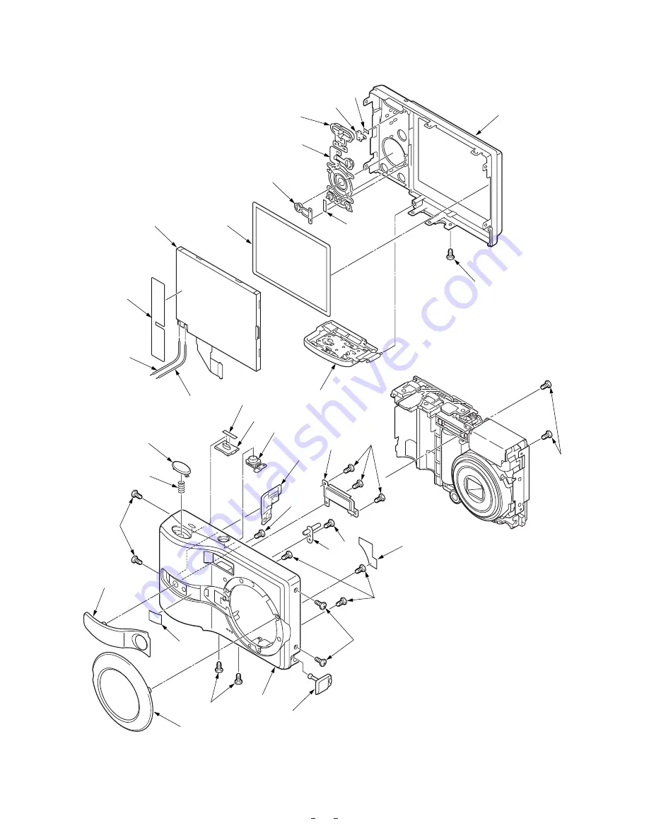
Page 25: ...25 CABINET AND CHASSIS PARTS 1 SX81R J Parts List1 CABINET 1 1 2 3 4 5 6 7 8 9 10 11 12 13 14 15 16 17 18 19 20 21 22 23 24 25 26 27 101 101 103 104 104 104 105 104 102 ...
Page 26: ...0U A 300V 17 636 095 7220 SPACER CONDENSER SX8RR J 18 636 094 8334 ADHESIVE CONDENSER SX8RR 19 636 092 6783 LABEL CAUTION BATT A 813J 20 636 092 6769 LABEL CAUTION BATT B 813J 21 636 094 6897 HOLDER BATTERY SX8RR J 22 645 085 0141 ASSY LAMP SX8RR 23 636 094 6194 EARTH SHAFT SX8RR J 24 636 092 7452 SHAFT ZOOM SX88A JNK 25 636 094 6040 TERMINAL BATT B SX8RR J 26 636 094 6033 TERMINAL BATT A SX8RR J ...
Page 27: ...27 CABINET AND CHASSIS PARTS 2 SX81R J Parts List2 CABINET 2 1 2 3 4 5 6 7 9 10 11 8 12 13 15 14 16 17 18 19 20 21 22 23 25 26 27 28 29 30 31 24 104 104 104 104 104 104 104 108 108 104 106 107 104 104 ...
Page 28: ...09 624 7806 IC NJM2860F3 03 IC301 410 594 0605 IC UPD78F0532GA T 9EV A IC302 409 582 6200 IC BD4289FVM IC303 409 614 8608 IC XC61CN1502N IC501 409 656 1704 IC UPD168801K8 4E5 AT IC503 409 667 4909 IC XC62KS0PXXM IC541 409 623 9108 IC RD3CYD08CM IC901 409 625 9304 IC CXD3443GA BGA N S P IC904 409 624 7806 IC NJM2860F3 03 IC905 409 604 8700 IC AD9949AKCPZ IC951 409 670 0608 IC LB8659P B E PHOTO DIOD...
Page 29: ...AMIC 1000P K 50V C9015 403 342 3300 CERAMIC 0 1U K 25V C9016 403 356 4706 CERAMIC 0 15U K 25V C9018 403 441 5700 TA SOLID 22U M 10V C9019 403 338 0306 CERAMIC 0 1U K 10V C9021 403 441 5700 TA SOLID 22U M 10V C9024 403 338 0306 CERAMIC 0 1U K 10V C9025 403 342 3300 CERAMIC 0 1U K 25V C9026 403 342 3300 CERAMIC 0 1U K 25V C9037 403 397 7605 CERAMIC 1U K 25V C9038 403 342 3300 CERAMIC 0 1U K 25V C903...
Page 30: ...45 083 5902 SWITCH PUSH 1P 1T S3010 645 083 5902 SWITCH PUSH 1P 1T RECHARGEABLE BATTERY Z3001 645 051 6009 BATTERY RECHARGE VARISTOR VA131 408 050 1204 VARISTOR AVR M1608C120MT FUSES F5001 423 031 1707 FUSE 32V 2A F5002 423 031 1707 FUSE 32V 2A F5003 423 031 1707 FUSE 32V 2A F5004 423 031 1707 FUSE 32V 2A CONNECTORS CN110 645 075 9741 SOCKET 8P N S P CN143 645 078 5856 SOCKET CARD SD 1 N S P CN171...
Page 31: ...31 1 2 3 4 Fig 6 1 Accessories ...
Page 32: ... CIRCUIT C5 SYSTEM CONTROL CIRCUIT C6 POWER CIRCUIT C7 STROBO CIRCUIT C7 CIRCUIT DIAGRAMS MAIN LCD DRIVER CIRCUIT WAVEFORMS C7 CP1 BOARD DMA MAIN LCD DRIVER LENS C8 CP1 BOARD CAA CCD DRIVER C13 CP1 BOARD SYA SYSTEM CONTROL C14 CP1 BOARD PWA POWER C15 CP1 BOARD STA STROBO C18 TB1 BOARD SWITCH TOUCH SENSOR C19 PRINTED WIRING BOARDS P W B TB1 P W B SIDE A B C19 CP1 P W B SIDE A B C20 ...
Page 33: ...IATE FROM THE RESISTANCE WATTAGE AND VOLT AGE RATINGS SHOWN EXPLANATORY NOTES EXAMPLES Resistor 10K 1 16J means 10kilo ohm 5 1 16watt max 1M 1 10K means 1mega ohm 10 1 10watt max Capacitor 0 047 F means 0 047micro farad Ftype Electrolytic capacitor 10 16 means 10micro farad 16volt max Inductor 330 J means 330micro henry 5 470 K means 470micro henry 10 No description J or K means 5 Figure of printe...
Page 34: ...6 29 D7 30 GND 31 CLK 32 VD 33 HD CSYNC 34 RESET 35 LOAD Z1 Z2 36 SCLK 37 SDATA 10 AFPI_E 4 IRIS 11 ZMPI_K 5 IRIS 12 ZMPI_V 6 SHUT 13 ZMPI_E 7 SHUT 14 ZM 8 AFPI_K 15 ZM 9 AFPI_V 16 AFSPM 2 A 17 AFSPM 4 B 1 ZMPR_V 2 ZMPR_K 3 ZMPR_E 18 AFSPM 1 A Z1 Z2 19 AFSPM 3 B 10 CARD 4 VDD 11 CARD WP 5 CLOCK 12 WP 6 VSS 7 DATA0 8 DATA1 9 DATA2 1 DATA3 2 COMMAND 3 VSS Z1 Z2 Z3 Z4 4 ZAV_JACK 5 USB D 6 GND 7 USB D...
Page 35: ...SERIAL SIG x3 CN110 AV USB IC132 EX OR USB_CONNECT Q9502 SW PLAY MENU MODE etc FLCTL R LED PHOTO TR R R Xe FLASH VALVE ILLUMI SELF_LED BOOST3 6V TO LENS BLOCK VDD3 VDD1 2 12V A 7 5V A IC303 BATOFF MIC SPEAKER RESET SX81R_ALL_BLOCK STA BLOCK CAMERA CIRCUIT LENS CCD EF 12V A 7 5V A ICX624AQN VDD VL H2B RG H2A VOUT O_LPF IC903 Q9001 SW SUBGT 18 28 17 CSUB 24 15 IC905 CDS AGC A D C AD 0 11 40 1 4 7 13...
Page 36: ... 0 CN110 AV USB VIDEO AMP IC151 YOUT AUDIO CODEC IC181 SPEAKER MIC FLASH SX81R_MAIN_BLOCK TOUCH SENSOR AA18 V16 Y17 W17 U3 A11 A10 IC78F0532GA T 9EV E1 T21 Y19 R17 R18 T20 F18 W18 Y18 V3 T22 G19 H22 H21 N1 U4 A7 A8 L22 L21 L20 KFG5616U1A K4S563233F WM8974 GEFL RV MAX9502GEXK 16 5 1 ICX624AQN N5 N4 U2 12 IN11 PRCTL IC101 J21pin AFPI ZMPR VB1 VB2 LD PI A ZOOM PI A 13 11 8 10 17 19 16 18 25 26 27 28 ...
Page 37: ... BACKUP BAT OFF AL3 2V UNREG VDD RESET 1 2 3 4 AL3 2V BACK UP SI MENU TELE SCANIN1 SCANIN2 26 SCANIN3 UP SW3 2ON Q3002 SCAN_OUT2 VDD 47 AVREF 2nd SCENE SCK 32 USB_CONNECT USB_DET2 17 MAIN RESET 22 COMREQ TO STA TO DMA TO PWA PLLEN SREQ ASIC_SDI ASIC_SDO SCK MRST ZBOOT_COMREQ Z3001 Q3001 BOOST3 6V BACKUP 3 2V UNREGSY IC303 RESET 50 57 VMONIT ST_CHG_ON VMONIT CHG 40 LCD PWM LCD PWM 30 PON PON 23 HOT...
Page 38: ...SHDNB4 4 5 30 LOUTA21 22 VDD3 TO DMA STA SYA 3 25V A SHDNB5 6 7 LOUTB21 22 BLON 28 SHDNB7 CH3 L5004 10 VDD1 2 LOUT3 CH7 L5005 Q5002 STEP UP CIRCUIT CH5 L5006 Q5001 STEP UP CIRCUIT CH4 L5007 Q5004 16 7 5V A OUT4 15 12V A OUT5 CH6 NC 13 LCDAN OUT7 42 LCDCA II71 PAON4 LCDPWM STEP UP CIRCUIT IC501 SWITCHING CONTROL UPD168801K8 4E5 E1 STEP UP DOWN CIRCUIT Q5009 Q5008 Q5003 Q5005 Q5007 STEP DOWN CIRCUIT...
Page 39: ...POC36 G18 GPOC37 H21 GPOC38 G19 GPOC39 H22 GPOC40 F20 GPOC41 F19 GPOC42 G20 GPOC43 E20 GPOC44 D20 GPOC45 H19 CVDD G21 LIOVDD3 G22 LCVDD F21 AFECKP F22 AFECKN E21 AFESD1P E22 AFESD1N C20 VIAS D21 AFESD2P D22 AFESD2N C21 LIOGND C22 LCGND F18 ADCK E19 CVDD C19 CCD0 F17 CCD1 B20 CCD2 E18 CCD3 B19 CCD4 E17 CCD5 A20 CCD6 C18 CCD7 A19 CCD8 B18 CCD9 A18 CCD10 C17 CCD11 B17 VCTRLEN F16 VSYNC A17 VSTDATA0 A...
Page 40: ...DATA5 A15 VSTDATA6 F15 VSTDATA7 E14 VSTEN B15 VSTREQ F14 ASTDATA D14 CVDD D13 ASTEN C14 ASTFLG E13 ASTREQ B14 VDATA0 F13 VDATA1 F12 VDATA2 A14 VDATA3 E12 VDATA4 C13 VDATA5 D12 VDATA6 F11 VDATA7 B13 VOUTCLK C11 VINCLK E11 A2VDD B12 A2VDD D11 A2GND C12 A2GND C10 REXT A13 RPU_ENA D10 UVDD B11 UGND A12 FSDP A11 HSDP A10 HSDM A9 FSDM B10 UGND D9 UVDD B9 VBDET A8 XIN A7 XOUT E10 PSEL C9 CLKSEL E9 PLLTES...
Page 41: ...1 V22 GPOF22 T18 GPOF23 T19 GPOF24 U21 GPOF25 T21 GPOF26 T20 GPOF27 R17 GPOF28 R18 GPOF29 U19 CVDD T22 CSYNC R19 GPOB4 R21 GPOB5 R20 GPOB6 R22 GPIOB0 P20 GPIOB1 P19 GPIOB2 P21 GPIOB3 P18 GPIOC0 P22 GPIOC1 P17 GPIOC2 N20 GPIOC3 N19 GPIOC4 N21 GPIOC5 N18 GPIOC6 N22 GPIOC7 N17 GPIOC8 M20 GPIOC9 M19 GPIOC10 M21 GPIOC11 M18 GPIOC12 M17 GPIOC13 M22 GPIOC14 L17 GPIOC15 L22 GPIOC16 L21 GPIOC17 L20 GPIOC18...
Page 42: ...T A2 NC A3 NC A6 NC A7 NC A8 NC B1 NC B2 WE B3 RP B4 DQ14 B5 Vss B6 Vss B7 DQ13 B8 NC C1 NC C2 DQ12 C3 DQ8 C4 DQ1 C5 OE C6 DQ9 C7 Vcc C8 NC D2 DQ7 D3 DQ4 D4 DQ11 D5 DQ10 D6 DQ3 D7 Vcc E2 DQ15 E3 A12 E4 DQ0 E5 A15 E6 DQ5 E7 DQ6 F2 CLK F3 CE F4 DQ2 F5 NC F6 NC F7 A9 G2 A14 G3 A13 G4 AVD G5 A7 G6 A11 G7 A8 H1 NC H2 INT H3 A0 H4 A1 H5 NC H6 A10 H7 A6 H8 NC J1 NC J2 RDY J3 A4 J4 A5 J5 A2 J6 A3 J7 NC J8...
Page 43: ...1 VGA L4 GPOA0 P4 GPOA1 M6 GPOA2 U1 GPIOE0 N4 GPIOE1 U2 GPIOE2 N5 GPIOE3 U3 GPIOE4 T2 GPIOE5 P5 GPIOE6 V1 GPIOE7 T3 GPIOE8 W1 GPIOE9 V2 GPIOE10 P6 GPIOE11 T4 CVDD N6 GPIOA3 M5 GPIOA4 V3 GPOD0 R4 GPOD1 W2 GPOD2 R5 GPOD3 Y1 GPOD4 Y2 GPOD5 R6 GPOD6 T5 GPOD7 T6 GPOD8 W3 GPOD9 U4 GPOD10 Y3 GPOD11 U5 GPOD12 U6 GPIOD13 W4 GPIOD14 V5 GPIOD15 V4 CVDD V6 IVDDWA W6 CVDDA V14 SD0 AB15 SD1 W14 SD2 AB16 SD3 AA1...
Page 44: ...7 8 1 2 3 4 5 6 7 8 1 2 3 4 C1 L2 L3 B1 D1 D2 E1 E2 F1 F2 G10 F11 F10 E11 E10 D11 K9 K11 J11 J10 H11 H10 G2 H1 H2 J1 J2 K1 B11 C11 L10 G1 L6 L8 L9 G11 K3 L7 L5 L4 B3 A3 B5 A7 B7 B9 C10 A9 B8 A8 B6 A5 B4 A2 C2 A10 A6 A4 K4 K5 K6 K7 K8 D10 Z1 Z2 Z3 Z4 1 2 3 4 1 2 3 4 1 2 3 4 5 6 1 2 3 4 1 2 3 4 5 6 7 8 9 10 11 12 13 14 15 VOUT 16 VDD 17 18 19 20 GND 21 GND 22 GND 23 24 CSUB 25 NC 26 VL 27 28 1 D1 2 ...
Page 45: ...0 S3009 10 LAND_BTOB_01_10_S CN301 UP0KG8D00L Q3001 330 RB304 MRST 1K RB301 1K RB301 1K RB301 1K RB301 32 768KHz 1AV4V10B7880G X3002 0 RB316 10K RB314 R3001 330K 1 16D IC78F0532GA T 9EV E1 A QXXAGF532GA9G IC301 1 2 3 4 1 2 3 4 1 2 3 4 1 VOUT 2 VIN 3 NC 4 VSS 1 2 3 4 5 6 7 8 1 2 3 4 5 6 7 8 1 2 3 4 1 2 3 4 5 6 7 8 1 2 3 4 10 SCANOUT2 4 TSEN_LED 5 TSEN_PULSE 6 TOUCH_IN 7 SCANIN4 8 SCANIN1 9 SCANIN0 ...
Page 46: ...A 1 B C5009 0 1 B C5016 2SA2029 R Q5005 1 B C5305 10 B 1608 C5303 20 1 16D R5030 2 2 B 1608 C5019 1 3K 1 16D R5019 390K 1 16D R5306 PAON2 1 2K 1 16D R5011 6 2K 1 16D R5008 33K 1 16D R5006 100 1AV4L26B3450G 2125 MPZ2012S101AT L5010 0 1 16Z R5038 CTRL1 PAON4 XC62KS0PXXMR QXC62KS0PXXMP IC503 2 2 B CK1C225KGQBNG 1608 C5024 DTC143ZM Q5013 10K 1 16D R5018 MTM231230L Q5014 SP_VDD 27K 1 16D R5022 300K 1 1...
Page 47: ... 2A32V F5001 1 B C5009 1 B C5305 10 B 1608 C5303 390K 1 16D R5306 1 2K 1 16D R5011 6 2K 1 16D R5008 33K 1 16D R5006 100 1AV4L26B3450G 2125 MPZ2012S101AT L5010 0 1 16Z R5038 150K 1 16D R5302 1 SCP 2 VPIN21 3 VPIN22 4 LOUTA21 5 LOUTA22 6 LOUTB21 7 LOUTB22 8 PGND2 9 PGND3 10 LOUT3 11 VPIN3 12 PGND4 13 OUT7 14 OUT6 15 OUT5 16 OUT4 17 PVDD 18 DOUT11 19 DOUT12 20 LOUT11 21 LOUT12 22 PGND11 23 PGND12 24 ...
Page 48: ... 36K 1 16J R5033 EMH11 Q5003 LCDPWM BOOST3 6V AWG30 2 0X1 25 JW534 130K 1 16D R5028 2 2 B 16 1608 C5015 510K 1 16J R5032 SCH2819 Q5002 7 5V A 0 1 B C5016 2SA2029 R Q5005 20 1 16D R5030 2 2 B 1608 C5019 1 3K 1 16D R5019 PAON2 CTRL1 PAON4 XC62KS0PXXMR QXC62KS0PXXMP IC503 2 2 B CK1C225KGQBNG 1608 C5024 DTC143ZM Q5013 10K 1 16D R5018 MTM231230L Q5014 SP_VDD 27K 1 16D R5022 300K 1 16D R5024 330K 1 16D ...
Page 49: ...G T5401 0 068 B 1608 C5407 100 1 16D R5407 120 1 16D R5408 1 2K 1 16J R5409 1K RB542 10K RB541 10K RB541 0 01 350B CK2V103KSPBNG 3216 C5404 RR255M 400TR D5404 HAP180N140D D5402 100K 1 8J X 3216 RGXAGE104JZKG R5406 UNREGST CHG VMONIT VDD3 FLCTL 12V A 10M 1 4F X RGXAVB106FDAP 2125 R5404 _NDM AWG28 2 2X1 5 JW549 PINK AWG28 2 2X1 5 JW550 BLACK 33 6 3 V CV0J330MAEANG 3 5X2 8 C5408 120 300 E C5412 0 018...
Page 50: ...GND FGND FGND 1M 1 16J 1608 R3305 0 1 16Z R3310 2PC4617R_115 Q3301 6 8K RB331 6 8K RB331 10K 1 10J 2125 R3308 SHUTTER CL331 1 2 3 4 1 2 3 4 1 2 3 4 5 6 10 SCANOUT2 4 TSEN_LED 5 TSEN_PULSE 6 TOUCH_IN 7 SCANIN4 8 SCANIN1 9 SCAN IN0 1 GND 2 GND 3 VDD3 1 2 3 4 TB1 T1 04901 SX81R U TO CP1 SYA CN301 POWER TOUCH SENSOR CIRCUIT TB1 BOARD SWITCH TOUCH SENSOR PRINTED WIRING BOARDS P W B TB1 P W B SIDE A SX8...
Page 51: ...L512 CL513 CL514 Q5004 CL516 CL517 CL518 CL519 CL901 CL520 CL521 CL522 CL523 CL524 CL525 CL331 CL332 CL333 C5404 CL334 CL529 CL335 Q5402 CL336 CL338 D5002 D5003 D5004 RB101 RB102 RB103 CL154 CL541 CB901 CB902 CL543 CB903 CL544 CB904 CL545 RB301 CL546 RB302 CL547 RB303 CL548 RB304 D5401 CL161 D5404 X3001 R5402 X3002 R5404 R5406 RB313 RB314 RB315 CL174 CL176 RB127 CL177 CL179 RB901 CL182 RB132 RB902...
Page 52: ...Feb 06 SANYO Electric Co Ltd Osaka Japan Printed in Japan ...