background image

– 7 –

47

/DC_IN

I

See next page 

1-4. SYA CIRCUIT DESCRIPTION

1. Configuration and Functions

For the overall configuration of the SYA block, refer to the block diagram. The SYA block centers around a 8-bit microprocessor
(IC301), and controls camera system condition (mode).
The 8-bit microprocessor handles the following functions.
1. Operation key input, 2. Clock control and backup, 3. Power ON/OFF, 4. Storobe charge control, 5. Signal input and output for
zoom and lens control.

Pin

Signal

1~4

5

6

7

8

9

10

11

12

14

15

16

17

18

19

20

21

22

23

30

32

33

34

35

36

37

38

39

40

41

42

43

45

44

46

/SCAN OUT 0~3

P ON

PA ON

BL_ON

LCD_ON

VSS

VDD

/SELF LED

/STBY_LED (GREEN)

/AVREF_ON

SI

SO

SCK

PRG SI

PRG SO

PRG SCK

NOT USED

NOT USED

CHG ON

NOT USED

CHG VOL

BATTERY

AVREF

AVDD

/RESET

XCOUT

XCIN

IC

XOUT

XIN

VSS

/BAT OFF

/SREQ

/SCAN IN3

SUB 1

I/O

O

O

O

O

O

-

-

O

O

O

I

O

I/O

I

O

I/O

-

-

O

-

I

I

-

-

I

O

I

I

O

I

-

I

I

I

I

Outline

Key scan output

Digital power ON/OFF control

H : ON

Analog power ON/OFF control

H : ON

LCD backlight ON/OFF control

H : ON

LCD power ON/OFF control

H : ON

GND

VDD

Stand-by LED (green) control

L : ON

A/D converter standard voltage control

L : ON

Receiving data (from ASIC)

Sending data (to ASIC)

Communication clock (to ASIC)

Flash memory writing receiving data

Flash memory writing sending data

Flash memory writing communication clock

-

-

-

Storobe charge voltage detection (analog input)

Battery voltage detection (analog input)

Analog standard voltage input terminal

A/D converter analog power terminal

Reset input

Clock oscillation terminal (37.768 kHz)

Clock oscillation terminal

Flash memory writing voltage

Main clock oscillation terminal (4MHz)

Main clock oscillation terminal

GND

Battery OFF detection

Serial communication requirement (from ASIC)

Key scan input 6

Command input (from ASIC)

DC jack/battery detection input

Flash charge control

H : ON

13

/STBY_LED (RED)

O

Stand-by LED (red) control

L : ON

24

VDD

-

VDD

25

AVSS

-

AVSS

27~29

SCAN IN 0~2

I

Key scan input

Self LED (red) control

L : ON

31

NOT USED

-

-

26

NOT USED

-

-

Summary of Contents for Xacti VPC-S1

Page 1: ...ce to product safety Should any component designated by a symbol need to be replaced use only the part designated in the Parts List Do not deviate from the resistance wattage and voltage ratings shown CAUTION Danger of explosion if battery is incorrectly replaced Replace only with the same or equivalent type recommended by the manufacturer Discard used batteries according to the manufacturer s ins...

Page 2: ...ster transfer clock Vertical register transfer clock Vertical register transfer clock Horizontal register transfer clock Reset gate clock Horizontal register transfer clock GND Signal output Circuit power Waveform DC Voltage 7 5 V 0 V 7 5 V 0 V 15 V 7 5 V 0 V 7 5 V 0 V 15 V 15 V 0 V 3 0 V 0 V 3 0 V Table 1 1 CCD Pin Description GND 0 V Aprox 10 V 13 0 V 16 V When sensor read out Vø5A Vø5B Note Not...

Page 3: ... 1 Iris drive When the drive signals IIN and IIN which are output from the ASIC IC101 it is driven by the driver IC951 and are then used to drive the iris steps 5 2 Focus drive When the drive signals FIN_A FIN_ A FIN_B and FIN_ B which are output from the ASIC expansion I O port IC105 the focus stepping motor is driven by the driver IC951 De tection of the standard focusing positions is carried ou...

Page 4: ...e reset signals ASIC and CPU and the serial signals take a picture commands from the 8 bit microprocessor are input and operation starts When the TG SG drives the CCD picture data passes through the A D and CDS and is then input to the ASIC as 10 bit data The AF AE AWB shutter and AGC value are com puted from this data and three exposures are made to obtain the optimum picture The data which has a...

Page 5: ...r which is connected to Pin 37 of IC501 all output is turned off The control signal P ON are recontrolled to restore output 3 Analog System Power Output 15 0 V A 7 6 V A and 3 05 V A are output Feedback for the 15 0 V A is provided to the switching controller Pin 40 of IC501 so that PWM control can be carried out 4 Digital 1 8 V Power Output 1 8 V D is output Feedback for the 1 8 V D is provided t...

Page 6: ...ltage alternating current which is generated at the secondary side of T5401 is rectified to produce a high voltage direct current and is accumulated at electrolytic ca pacitor C5412 1 6 Voltage monitoring circuit This circuit is used to maintain the voltage accumulated at C5512 at a constance level After the charging voltage is divided and converted to a lower voltage by R5417 R5419 and R5420 it i...

Page 7: ...ey scan output Digital power ON OFF control H ON Analog power ON OFF control H ON LCD backlight ON OFF control H ON LCD power ON OFF control H ON GND VDD Stand by LED green control L ON A D converter standard voltage control L ON Receiving data from ASIC Sending data to ASIC Communication clock to ASIC Flash memory writing receiving data Flash memory writing sending data Flash memory writing commu...

Page 8: ...fication 63 64 ZTEST ASIC RESET O O ASIC reset signal L RESET CPU reset singal L RESET 61 62 51 I Beep output 52 BUZZER O USB connector detection L USB detecion 57 PLLEN O PLL reset signal L RESET USB CLKSEL 1 O CPU clock swtich control 59 60 CARD I SD card insertion detection L Insertion NOT USED CLKSEL 0 O CPU clock ON OFF control H ON 49 AV JACK I AV jack connection detection H AV jack detectio...

Page 9: ... can start up again When the battery is removed the 8 bit micro processor operates in sleep mode using the backup lithium secondary battery At this time the 8 bit microprocessor only carries out clock counting and waits in standby for the battery to be attached again When a switch is operated the 8 bit microprocessor supplies power to the system as required The 8 bit microprocessor first sets both...

Page 10: ...2 Cabinet back 3 Cover battery 4 Cabinet front 5 Shield tape top 2 6 Spacer holder B 7 Spacer chassis 8 Two screws 1 7 x 4 9 FPC 10 TB1 board 11 FPC 12 Remove the solder 13 LCD 14 Two screws 1 7 x 4 15 Holder monitor 1 1 1 2 3 4 5 6 7 1 8 9 10 11 12 13 14 14 15 B A When assembling tighten screws A B ...

Page 11: ... 3 Remove the solder 4 Spring earth A 5 Screw 1 7 x 4 6 Three screws 1 4 x 3 5 7 Three screws 1 7 x 4 8 Lens assembly 9 CP1 board TB1 board CP1 board A A 1 2 3 4 5 6 8 7 9 A C B When assembling tighten screws A B C When changing the lens and CCD disassemble after removing solder at CCD ...

Page 12: ... software installation diskette into your diskette drive 2 Open the explorer 3 Copy the DscCalDI_130b folder on the floppy disk in the FD drive to a folder on the hard disk 3 Installing USB driver Install the USB driver with camera or connection kit for PC 4 Pattern box color viewer Turn on the switch and wait for 30 minutes for aging to take place before using Color Pure It is used after adjustin...

Page 13: ...he computer 1 Line up the arrow on the cable connector with the notch on the camera s USB port Insert the connector 2 Locate a USB port on your computer 3 Set the main switch to PC and turn on the camera AC adaptor To USB port USB cable ...

Page 14: ...3 size siemens star chart Fluorescent light illumination with no flicker Illumination above the subject should be 400 lux 10 Adjustment method 1 Set the siemens star chart 100 cm 3 cm so that it be comes center of the screen 2 Double click on the DscCalDi exe 3 Click the Focus and click the Yes 4 Lens adjustment value will appear on the screen 5 Click the OK Adjustment value determination is effec...

Page 15: ...s other than the above are irrelevant 4 CCD White Point Defect Detect Adjustment Preparation POWER switch ON Adjustment method 1 Double click on the DscCalDi exe 2 Select CCD Defect on the LCD Test and click the Yes 3 After the adjustment is completed OK will display 4 Click the OK 5 CCD Black Point And White Point Defect Detect Adjustment In Lighted Preparation POWER switch ON Setting of pattern ...

Page 16: ... the DscCalDi exe 2 Adjust LCD VCOMPP so that the amplitude of the CL404 waveform is 5 45 V 0 1 Vp p 6 2 LCD VcomDC Adjustment Adjusting method 1 Adjust LCD VCOMDC so that the amplitude of the CL404 waveform is 4 02 V 0 05 Vp p 5 45 V 0 1 Vp p CL404 waveform 4 02 V 0 05 Vp p GND CL404 waveform ...

Page 17: ...USB storage window and check the USB storage data VID SANYO PID VPC S1 Serial Rev 1 00 4 Check the Serial in the above USB storage data If the displayed value is different from the serial number printed on the base of the camera enter the number on the base of the camera Then click the Set button 5 Next check VID PID and Rev entries in the USB storage data If any of them are different from the val...

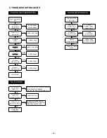
Page 18: ...E INPUT CHECK S6001 CN601 CN301 D3011 CN301 5 6 P ON P A ON CHECK IC301 RB301 SERIAL COMMUNICATION CHECK IC301 CP1 DMA BLOCK CHECK CP1 DMA BLOCK TAKING INOPERATIVE NO NO LOW LOW LOW NO NO YES YES HIGH HIGH HIGH YES YES YES HIGH OK NO LOW NG NO PICTURE MAIN CLOCK FOR SYSTEM OPERATION NO OPERATION IF ABSENT CHECK X1101 OSCILLATOR AND IC111 CLK 98 MHz INPUT TO IC101 5 CLK IN 1 CLK 48 MHz INPUT TO IC1...

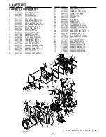
Page 19: ...071 8432 SPACER HOLDER B SX714 U 29 636 073 6047 ASSY WIRE BAT SX743 30 636 071 9477 COMPL PWB TB 1 31 636 074 2444 SHIELD TAPE TOP2 SX714 U 32 645 061 9779 FLEXIBLE FLAT CABLE 33 636 073 6948 SPACER FUSE SX714 U 34 645 061 7973 OPTICAL FILTER 35 636 071 3970 SPACER 36 409 545 8401 IC ICX432JQ C 37 636 071 3963 MOUNTING LENS 38 636 071 9460 COMPL PWB CP 1 39 636 071 8425 SPACER HOLDER A SX714 U 40...

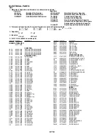
Page 20: ...R EMF18 Q5401 405 115 7508 TR DTC123JE Q5402 405 169 4508 TR DTC114EM OR 405 172 4601 TR UNR32A1 Q5405 405 170 0308 TR CPH5504 E Q5407 405 152 5406 TR 3LN01S TL Q5409 405 171 4800 TR CY25BAJ 8F Q5410 405 102 6705 TR 2SA1745 7 OR 405 102 8303 TR 2SA1745 6 Q5411 405 168 3700 TR DTC144EM OR 405 172 4700 TR UNR32A3 Q9002 405 153 6709 TR 2SC3931 D Q9003 405 102 5609 TR 2SD1819A R OR 405 092 4101 TR 2SC...

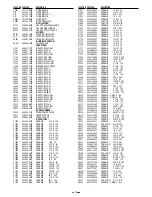
Page 21: ...403 332 9503 CERAMIC 1U M 6 3V C1306 403 332 9503 CERAMIC 1U M 6 3V C1501 403 311 5007 CERAMIC 33P J 50V C1502 403 369 0306 CERAMIC 1U Z 4V C1503 403 332 9503 CERAMIC 1U M 6 3V C1504 403 345 3802 TA SOLID 22U M 4V C1505 403 345 4205 TA SOLID 47U M 6 3V C1506 403 332 9503 CERAMIC 1U M 6 3V C1507 403 311 7506 CERAMIC 22P J 50V C1701 403 332 9503 CERAMIC 1U M 6 3V C1702 403 332 9503 CERAMIC 1U M 6 3V...

Page 22: ...TWORK 10KX4 1 32W RB142 645 028 0719 R NETWORK 10KX4 1 32W OR 645 036 0978 R NETWORK 10KX4 1 32W RB301 645 032 8886 R NETWORK 47KX4 1 32W OR 645 032 8879 R NETWORK 47KX4 1 32W RB302 645 032 8886 R NETWORK 47KX4 1 32W OR 645 032 8879 R NETWORK 47KX4 1 32W RB303 645 032 8886 R NETWORK 47KX4 1 32W OR 645 032 8879 R NETWORK 47KX4 1 32W RB304 645 028 0719 R NETWORK 10KX4 1 32W OR 645 036 0978 R NETWORK...

Page 23: ...0K JKG 1 8W R5426 401 225 9005 MT GLAZE 470K JA 1 16W R5429 401 261 3005 MT FILM 6 2K DU 1 16W R5430 401 225 1207 MT GLAZE 4 7K JA 1 16W R5431 401 224 8900 MT GLAZE 100K JA 1 16W R5432 401 261 2909 MT FILM 5 6K DU 1 16W R5433 401 224 8900 MT GLAZE 100K JA 1 16W R9003 401 226 1503 MT GLAZE 0 000 ZA 1 16W R9004 401 240 9004 MT GLAZE 3 9 JA 1 16W R9005 401 240 9509 MT GLAZE 820 JA 1 16W R9006 401 224...

Page 24: ...81 See 2 636 072 5348 CASE SOFT SX714 U 645 063 1917 DISC CD ROM SSP 714 U Sanyo Sofware Pack 6 5 N S P 636 069 5337 STRAP HAND SX711 J See 3 9112 636 072 6758 INSTRUCTION MANUAL CAMERA English 9113 636 072 6765 INSTRUCTION MANUAL Sanyo Sofware Pack 6 5 English 9151 645 058 8082 CARD MEMORY 16MB N S P 645 061 3357 CARD MEMORY 16MB N S P PACKING MATERIALS 636 072 3702 CARTON CASE INNER SX714 U 636 ...

Page 25: ......

Page 26: ...Aug 03 SANYO Electric Co Ltd Osaka Japan ...

Reviews: