


10-2
Samsung Electronics
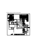
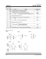
IC Internal Diagram
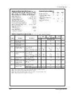
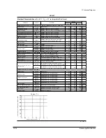
Absolute Maximum Ratings
(Notes 1 @ 2)
If Military.Aerospace specified devices are required0
please contact the National Semiconductor Sales
Office.Distributors for availability and specifications1
Supply Voltage (V
CC
)
b
0(5 to
a
7(0V
DC Input Voltage (V
IN
)
b
1(5 to V
CC
a
1(5V
DC Output Voltage (V
OUT
)
b
0(5 to V
CC
a
0(5V
Clamp Diode Current (I
IK
* I
OK
)
g
20 mA
DC Output Current* per pin (I
OUT
)
g
35 mA
DC V
CC
or GND Current* per pin (I
CC
)
g
70 mA
Storage Temperature Range (T
STG
)
b
65
C to
a
150
C
Power Dissipation (P
D
)
(Note 3)
600 mW
S(O( Package only
500 mW
Lead Temperature (T
L
)
(Soldering 10 seconds)
260
C
OperatingConditions
Min
Max
Units
Supply Voltage (V
CC
)
4(5
5(5
V
DC Input or Output Voltage
0
V
CC
V
(V
IN
* V
OUT
)
Operating Temp( Range (T
A
)
MM74HCT
b
40
a
85
C
Input Rise or Fall Times
(t
r
* t
f
)
500
ns
DC Electrical Characteristics
(V
CC
e
5V
g
10%* unless otherwise specified()
T
A
e
25
C
74HCT
T
A
e
125
C
Symbol
Parameter
Conditions
T
A
eb
40 to 85
C
Units
Typ
Guaranteed Limits
V
IH
Minimum High Level
2(0
2(0
2(0
V
Input Voltage
V
IL
Maximum Low Level
0(8
0(8
0(8
V
Input Voltage
V
OH
Minimum High Level
V
IN
e
V
IH
or V
IL
Output Voltage
l
I
OUT
l
e
20
m
A
V
CC
V
CC
b
0(1
V
CC
b
0(1
V
CC
b
0(1
V
l
I
OUT
l
e
6(0 mA* V
CC
e
4(5V
4(2
3(98
3(84
3(7
V
l
I
OUT
l
e
7(2 mA* V
CC
e
5(5V
5(2
4(98
4(84
4(7
V
V
OL
Maximum Low Level
V
IN
e
V
IH
or V
IL
Voltage
l
I
OUT
l
e
20
m
A
0
0(1
0(1
0(1
V
l
I
OUT
l
e
6(0 mA* V
CC
e
4(5V
0(2
0(26
0(33
0(4
V
l
I
OUT
l
e
7(2 mA* V
CC
e
5(5V
0(2
0(26
0(33
0(4
V
I
IN
Maximum Input
V
IN
e
V
CC
or GND*
g
0(1
g
1(0
g
1(0
m
A
Current
V
IH
or V
IL
* Pin 1 or 19
I
OZ
Maximum TRI-STATE
V
OUT
e
V
CC
or GND
g
0(5
g
5(0
g
10
m
A
Output Leakage
G
e
V
IH
Current
I
CC
Maximum Quiescent
V
IN
e
V
CC
or GND
8
80
160
m
A
Supply Current
I
OUT
e
0
m
A
V
IN
e
2(4V or 0(5V (Note 4)
0(6
1(0
1(3
1(5
mA
Note 16
Absolute Maximum Ratings are those values beyond which damage to the device may occur(
Note 26
Unless otherwise specified all voltages are referenced to ground(
Note 36
Power Dissipation temperature derating E plastic ‘‘N’’ package9
b
12 mW
C from 65
C to 85
C(
Note 46
Measured per input( All other inputs at V
CC
or ground(
Summary of Contents for Wingo S-2450
Page 2: ...ELECTRONICS Samsung Electronics Co Ltd SEP 2000 Printed in Korea Code no AH68 00036D ...
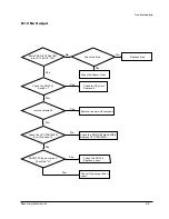
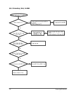
Page 14: ...Samsung Electronics 5 1 5 Block Diagram 5 1 Main ...
Page 17: ...6 2 Samsung Electronics 6 4 Jack PCB 6 5 Motor PCB 6 6 POWER S 2400 2450 ...
Page 18: ...Samsung Electronics 6 3 6 7 MAIN ...
Page 19: ...6 4 Samsung Electronics 6 8 CD 6 9 MP3 Charge MP3 Jack ...
Page 20: ...Samsung Electronics 6 5 6 10 Adapter Batt Sense 6 11 ENCODER ...
Page 21: ...ENCODER PCB DIAGRAM only S2450 Model ...
Page 22: ...ENCODER PCB DIAGRAM only S2450 Model ...
Page 23: ...Samsung Electronics 7 1 7 Wiring Diagram Optical Output Option NCW100 ...
Page 24: ...Samsung Electronics 8 1 8 Schematic Diagram 8 1 Main Part ...
Page 25: ...8 2 Samsung Electronics 8 2 CD ...
Page 26: ...Samsung Electronics 8 3 8 3 ENCODER ...
Page 27: ...ENCODER SCHEMATIC DIAGRAM only S2450 Model ...
Page 28: ...ENCODER SCHEMATIC DIAGRAM only S2450 Model ...
Page 41: ...Samsung Electronics 10 5 IC Internal Diagram Audio ICs BA3121 BA3121F BA3121N FBlock diagrams ...
Page 47: ...Samsung Electronics 10 11 IC Internal Diagram Audio ICs BU1923 BU1923F FBlock diagram ...
Page 56: ...10 20 Samsung Electronics IC Internal Diagram 10 11 TDA7440D JIC1 ...