background image

9-2

Samsung Electronics 

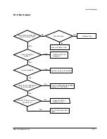
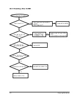
9-1-2 FLT Malfunction

 Connector inserted

correctly?

No

Check voltage : AC 2.6V 

at FRONT-PCB FLT?

No

Check Main-PCB Front PCB
connection and the voltage of
FCW2, pins2,3(AC 2.6V)

Check voltage at UIC1 

pin 51(-25V)

No

Check the voltage of AZD4,6(-25V)

Replace UIC1(LC866XXX)

Yes

Yes

Yes

Reinsert the connector

Troubleshooting

Summary of Contents for Wingo S-2450

Page 1: ...TERIOR COMPONENT SYSTME CONTENTS 1 Alignment and Adjustments 2 Disassembly and Reassembly 3 Exploded Views and Parts List 4 Electrical Parts List 5 Block Diagrams 6 PCB Diagrams 7 Wiring Diagram 8 Schematic Diagrams 9 Troubleshooting 10 IC Internal Diagram ...

Page 2: ...ELECTRONICS Samsung Electronics Co Ltd SEP 2000 Printed in Korea Code no AH68 00036D ...

Page 3: ...tenna 2 Remove Front Cabinet to frontward 1 Fig 2 1 1 Remove 6 screws of B its rear part 2 Remove the connect wire of C and remove Main PCB ASS Y to backward 3 Remove 3 screws of A its rear part and remove CD Mecha ASS Y to backward 2 2 Main PCB ASS Y AND CD MECHA ASS Y A B C Samsung Electronics Fig 2 2 ...

Page 4: ...ve 2 screws of A Deco Front 3 Remove 6 screws of B Cap Front 4 Remove Cap Front Ass y to frontward A B C C Fig 2 4 2 4 CAP Front ASS Y 1 Remove 2 screws of of its rear part 2 Pull up Cabinet Top Ass y to frontward and remove it 2 3 Cabinet Top ASS Y 1 Fig 2 3 ...

Page 5: ...ews and Parts List Samsung Electronics 3 1 1 2 4 14 5 3 12 13 15 16 17 7 8 9 6 10 18 19 20 21 22 24 28 29 23 25 26 27 30 FRONT PCB MAIN PCB TUNER PCB POWER PCB ENCORDER PCB Only S2450 POWER CORD CD PCB 11 CHARGE PCB ...

Page 6: ...15 AH64 00314A DECORATION SIDE R MIPS L GRAY S 2000 16 AH64 00307A CABINET FRONT MIPS D GRAY S 2000 17 AH61 00210A CAP CD ABS 94HB BLK S 2000 18 AH73 00007A RUBBER MECHA A BUTYL S 2000 19 AH73 00008A RUBBER MECHA B SILICONE S 2000 20 AH59 00038A DECK CDP DA23 2 0V BALL S 2000 21 AH73 00010A RUBBER HOLDER BUTYLENE S 2000 22 AH61 00213A HOLDER CD ABS GRAY S 2000 23 AH61 00217A HOLDER GEAR ABS BLK S ...

Page 7: ...TR45 2007 000282 R CHIP 100Kohm 5 1 10W DA TP 2012 TR47 2007 000282 R CHIP 100Kohm 5 1 10W DA TP 2012 TR49 2007 000282 R CHIP 100Kohm 5 1 10W DA TP 2012 TR9 2007 000282 R CHIP 100Kohm 5 1 10W DA TP 2012 TR24 2007 000290 R CHIP 100ohm 5 1 10W DA TP 2012 TR43 2007 000290 R CHIP 100ohm 5 1 10W DA TP 2012 TR2 2007 000300 R CHIP 10Kohm 5 1 10W DA TP 2012 TR21 2007 000300 R CHIP 10Kohm 5 1 10W DA TP 201...

Page 8: ...82 R CHIP 100KOHM 5 1 10W DA TP 2012 SR10 2007 000300 R CHIP 10KOHM 5 1 10W DA TP 2012 SR13 2007 000300 R CHIP 10KOHM 5 1 10W DA TP 2012 SR14 2007 000300 R CHIP 10KOHM 5 1 10W DA TP 2012 SR4 2007 000300 R CHIP 10KOHM 5 1 10W DA TP 2012 SR5 2007 000300 R CHIP 10KOHM 5 1 10W DA TP 2012 SR7 2007 000300 R CHIP 10KOHM 5 1 10W DA TP 2012 SR8 2007 000300 R CHIP 10KOHM 5 1 10W DA TP 2012 TR21 2007 000300 ...

Page 9: ...03080 CONNECTOR HEADER NOWALL 28P 1R 1 25 53434 2811 AH92 00223A ASSY PCB MOTOR S 2000 MOTOR BOARDNO A S MOTOR AH31 10021A MOTOR DC RF 500TB 9VDC 130mA AH66 10025A PULLEY MOTOR POM CMS 100 CCON2 3711 000826 CONNECTOR HEADER BOX 2P 1R 2MM ANGLE SN CCON3 3711 000826 CONNECTOR HEADER BOX 2P 1R 2MM ANGLE SN CC0N1 3711 000988 CONNECTOR HEADER 53015 0510 WHT AH92 00594A ASSY PCB MAIN S2450 W ENCODER AD1...

Page 10: ... 2401 002180 C AL 2 2uF 20 50V GP 5 11 5mm TP JC2 2401 002180 C AL 2 2uF 20 50V GP 5 11 5mm TP JC24 2401 002180 C AL 2 2uF 20 50V GP 5 11 5mm TP JC25 2401 002180 C AL 2 2uF 20 50V GP 5 11 5mm TP JC6 2401 002180 C AL 2 2uF 20 50V GP 5 11 5mm TP JC7 2401 002180 C AL 2 2uF 20 50V GP 5 11 5mm TP JC8 2401 002180 C AL 2 2uF 20 50V GP 5 11 5mm TP JC9 2401 002180 C AL 2 2uF 20 50V GP 5 11 5mm TP AL1 AH27 ...

Page 11: ...IAL 47nF 80 20 50V Y5V 3 5x19mm AUC26 2203 000239 C CERAMIC CHIP 100pF 5 50V NPO 2012 TP AUC22 2203 000979 C CERAMIC CHIP 47nF 10 50V X7R 2012 TP AUC19 2401 000240 C AL 100uF 20 10V GP 5 11mm 5mm TP BC12 2401 000778 C AL 220uF 20 10V GP 6 3x11 5MM TP AUC15 2401 001893 C AL 100uF 20 16V GP 6 7 5MM TP AUC11 2401 002180 C AL 2 2uF 20 50V GP 5 11 5mm TP EBD1 3301 000297 CORE FERRITE BEAD AA 3 6x1 2x5 ...

Page 12: ...2203 001619 C CERAMIC CHIP 27pF 5 50V NPO 2012 TP UC30 2401 000243 C AL 100uF 20 10V GP 6 5 2 5MM TP UC42 2401 000243 C AL 100uF 20 10V GP 6 5 2 5MM TP CU40 2401 000475 C AL 10uF 20 50V GP 5 11 5mm TP UC37 2401 000475 C AL 10uF 20 50V GP 5 11 5mm TP UC28 2401 000752 C AL 220nF 20 50V GP 3 5 2 5MM TP UC27 2401 001238 C AL 4 7uF 20 25V GP 3 5 2 5MM TP UC14 2401 001895 C AL 100uF 20 16V GP 6 3 11 5MM...

Page 13: ... 80 20 50V Y5V 2012 TP NC112 2203 001537 C CERAMIC CHIP 1NF 10 50V X7R 2012 NC113 2203 001537 C CERAMIC CHIP 1NF 10 50V X7R 2012 NC128 2203 001537 C CERAMIC CHIP 1NF 10 50V X7R 2012 NC136 2203 001537 C CERAMIC CHIP 1NF 10 50V X7R 2012 NC137 2203 001537 C CERAMIC CHIP 1NF 10 50V X7R 2012 NC103 2203 001551 C CERAMIC CHIP 1 5nF 10 50V X7R 2012 TP NC122 2203 001551 C CERAMIC CHIP 1 5nF 10 50V X7R 2012...

Page 14: ...Samsung Electronics 5 1 5 Block Diagram 5 1 Main ...

Page 15: ...22 24 23 31 35 36 37 38 40 MOTOR CONTROL S W SENSOR FOK MAIN PCB MAIN PCB MICOM CTRL LINE POWER AUDIO LINE 19 R L 20 36 37 38 68 25 26 30 29 10 70 72 73 75 76 27 MCK MDATA MLT ISTAT SQDT LKFS SOS1 SQCK A GND R CH L CH GND B RESET LOCK SMEF WDCH SMON SMSD SL IN SP IN TE IN EF IN VREF SL SL MOTOR ACTUATOR DRIVER 6 ASSP KB9223 NIC 9223 DIGITAL SIGNAL PROCESSOR 16 9344MHz 66 69 8 EFM TRCNT KA9258 NIC ...

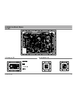
Page 16: ...Samsung Electronics 6 1 6 Printed Circuit Board Diagram 6 1 FRONT 6 2 Headphone PCB 6 3 Open Close PCB ...

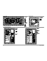
Page 17: ...6 2 Samsung Electronics 6 4 Jack PCB 6 5 Motor PCB 6 6 POWER S 2400 2450 ...

Page 18: ...Samsung Electronics 6 3 6 7 MAIN ...

Page 19: ...6 4 Samsung Electronics 6 8 CD 6 9 MP3 Charge MP3 Jack ...

Page 20: ...Samsung Electronics 6 5 6 10 Adapter Batt Sense 6 11 ENCODER ...

Page 21: ...ENCODER PCB DIAGRAM only S2450 Model ...

Page 22: ...ENCODER PCB DIAGRAM only S2450 Model ...

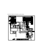
Page 23: ...Samsung Electronics 7 1 7 Wiring Diagram Optical Output Option NCW100 ...

Page 24: ...Samsung Electronics 8 1 8 Schematic Diagram 8 1 Main Part ...

Page 25: ...8 2 Samsung Electronics 8 2 CD ...

Page 26: ...Samsung Electronics 8 3 8 3 ENCODER ...

Page 27: ...ENCODER SCHEMATIC DIAGRAM only S2450 Model ...

Page 28: ...ENCODER SCHEMATIC DIAGRAM only S2450 Model ...

Page 29: ...1 Vp 23 5V Replace µ com Yes No FRONT PCB P OFF SENSE voltage normal pin 92 5 0V Check the Main PCB MCON5 FCW1 WIRE AD18 AZD3 No FRONT PCB UIC2 78L05 OUT 5V output voltage normal No No No Check the Main PCB AZD4 6 AZD5 25V normal Replace AZD4 5 6 No Replace µ com Yes Check the connector FRONT MAIN PCB FCW1 FCW2 Yes Replace µ com Yes Check the AQ2 D882 No Replace AQ2 TR D882 Yes Check the Fuse ...

Page 30: ...rrectly No Check voltage AC 2 6V at FRONT PCB FLT No Check Main PCB Front PCB connection and the voltage of FCW2 pins2 3 AC 2 6V Check voltage at UIC1 pin 51 25V No Check the voltage of AZD4 6 25V Replace UIC1 LC866XXX Yes Yes Yes Reinsert the connector Troubleshooting ...

Page 31: ...TDA7440D B of Function IC No Check the MCON5 CABLE WIRE Replace JIC1 TDA7440D No Main PCB AIC1 TA8270K pins 3 12 B 15 16V No Check the Fuse Check the Power Trans Yes No Replace Fuse FRONT PCB µ com pins 2 Check the H Yes Check the AQ1 3 4 Replace µ com Yes Restore sound with remocon No Check for TR short Replace it Yes Yes Troubleshooting ...

Page 32: ... focus search done properly Check pin 3 of KB9223 FRSH Check pin 48 of KB9223 FEO Check pin 1 2 of KA9258 Check pin 73 75 76 of KS9286 Check pin 23 24 25 of KB9223 Check pin 46 of KB9223 SPDLD Check pin 17 18 of KA9258 Check Spindle Motor of CD DECK Check pin 69 70 of KB9223 Check TR NQ100 Resistor NR14 Check Laser Diode of pick up Check pin 74 75 of KB9223 Check NC125 472 No No No No Yes Yes Yes ...

Page 33: ...4 75 76 77 Check Parts NC123 105Z NC124 472K NC125 472K NR125 472J NR126 183J Yes No Yes Yes Yes No No Check pin 53 54 50 49 of KB9223 Check pin 58 59 of KB9223 Check pin 26 27 of KA9258 Does it read Disc Check Parts NC110 NC90 NC89 END OK NG Change CD Deck Change IC Troubleshooting ...

Page 34: ... of BIC1 pin8 and condition Batt Sense of BQ10 Check condition of Batterise that peel off the sheath on the negative pole side from the new batteries by 5 mm using a knife before charging them Check collector B for A614 of BQ1 Replace A614 of BQ1 Check condition of BQ2 Yes No Yes No Check voltage line 5V for Vcc of Main No Yes No Yes Yes No Yes Check S W of Batt Sense and Batterise Spec NO Recharg...

Page 35: ... LCW1 MCW2 BCW3 Check voltage 5V for B of AUIC5 Check Lineof AC 3 Check High for pin3 6 20 of AUIC3 Check oscillation 24MHz of AUX1 Replace AUX1 Yes No Yes No Replace BF1 and BZD1 No Check voltage line 5V for Vcc of AQ1 No Yes Yes No Yes No Replace AUIC3 AUIC4 No Check circuit of AUIC3 AUIC4 and short Yes Check connction for Flat Cable from FCW1 to MCON5 NO PLAY ...

Page 36: ...ndition for EQ3 C945 High EQ2 R2003 Low Check Lineof AC 4 Recheck No Play of section previeous page Replace BCN5 Replace Encoder Pack Yes No Yes No Replace BF1 and BZD1 No Yes Yes No Yes Delete MP3 file of SMC Card No Check memory of SMC Card Yes Yes NOT Encoding from CD to MP3 Check voltage for P T Check connction for Connect Wire of EW1 Check condition for OP Amp of EIC1 ...

Page 37: ...as one active low enable input G and a direction control DIR When the DIR input is high data flows from the A inputs to the B outputs When DIR is low data flows from B to A MM74HCT devices are intended to interface between TTL and NMOS components and standard CMOS devices These parts are also plug in replacements for LS TTL devic es and can be used to reduce power consumption in exist ing designs ...

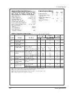
Page 38: ...meter Conditions TAeb40 to 85 C Units Typ Guaranteed Limits VIH Minimum High Level 2 0 2 0 2 0 V Input Voltage VIL Maximum Low Level 0 8 0 8 0 8 V Input Voltage VOH Minimum High Level VINeVIH or VIL Output Voltage lIOUTle20 mA VCC VCCb0 1 VCCb0 1 VCCb0 1 V lIOUTle6 0 mA VCCe4 5V 4 2 3 98 3 84 3 7 V lIOUTle7 2 mA VCCe5 5V 5 2 4 98 4 84 4 7 V VOL Maximum Low Level VINeVIH or VIL Voltage lIOUTle20 mA...

Page 39: ...o 85 C Units Typ Guaranteed Limits tPHL tPLH Maximum Output CL e 50 pF 17 23 29 34 ns Propagation Delay CL e 150 pF 24 30 38 45 ns tPZL Maximum Output RL e 1 kX 31 42 53 63 ns Enable Time CL e 50 pF tPZH Maximum Output RL e 1 kX 23 33 41 49 ns Enable Time CL e 50 pF tPHZ tPLZ Maximum Output RL e 1 kX 21 30 38 45 ns Disable Time CL e 50 pF tTHL tTLH Maximum Output CL e 50 pF 8 12 15 18 ns Rise and ...

Page 40: ...ng resistance and remove noise generated by the electrical devices used in automobiles The capacitance values of the external capacitors required for the ICs are small to allow compact and reliable set design FApplications Car audio systems FFeatures 1 Large capacitors not required 2 High common mode rejection ratio 57dB typ at f 1kHz 3 Low noise VNO 3 5µVrms Typ 4 Low distortion THD 0 002 Typ 5 T...

Page 41: ...Samsung Electronics 10 5 IC Internal Diagram Audio ICs BA3121 BA3121F BA3121N FBlock diagrams ...

Page 42: ...10 6 Samsung Electronics IC Internal Diagram Audio ICs BA3121 BA3121F BA3121N FElectrical characteristics unless otherwise noted Ta 25_C VCC 12V f 1kHz Rg 1 8kΩ ...

Page 43: ...ltage are outside configured limits Fast charge is terminated by any of the following n Peak voltage detection PVD n Negative delta voltage V n Maximum voltage n Maximum temperature n Maximum time After fast charge the bq2002 F op tionally tops off and pulse trickles the battery per the pre configured limits Fast charge may be inhibited using the INH pin The bq2002 F may also be placed in low stan...

Page 44: ...ckle Functional Description Figure 2 shows a state diagram and Figure 3 shows a block diagram of the bq2002 F Battery Voltage and Temperature Measurements Battery voltage and temperature are monitored for maximum allowable values The voltage presented on the battery sense input BAT should represent a single cell potential for the battery under charge A resistor divider ratio of RB1 RB2 N 1 is reco...

Page 45: ...01 VTS VCC 2 VTS VCC 2 VBAT 2V VBAT 2V VTS VCC 2 VTS VCC 2 PVD or V or Maximum Time Out and TM high PVD or V or Maximum Time Out and TM high Figure 2 State Diagram OSC TM CC LED VCC VSS BAT INH Clock Phase Generator Timing Control Sample History A to D Converter MCV Check TS Bd2002f eps Voltage Reference PVD V ALU Power On Reset TCO Check Power Down Charge Control State Machine Figure 3 Block Diag...

Page 46: ...or filter Linear CMOS circuitry is used for low power consumption FApplications RDS RBDS compatible FM receivers for American and European markets car stereos high fidelity stereo systems and components and FM pagers FFeatures 1 Low current 2 Two stage anti aliasing filter LPF 3 57kHz band pass filter 4 DSB demodulation digital PLL 5 Quality indication output for demodulated data FAbsolute maximum...

Page 47: ...Samsung Electronics 10 11 IC Internal Diagram Audio ICs BU1923 BU1923F FBlock diagram ...

Page 48: ...10 12 Samsung Electronics IC Internal Diagram Audio ICs BU1923 BU1923F FPin descriptions FInput output circuits ...

Page 49: ...onents required Adjacent channel interference rejection function third and fifth order Supports both the SD and the IF counting techniques The AM and FM SD sensitivities can be set independently The AM and FM output levels can be set independently Improved AM practical sensitivity and high input distortion characteristics Package Dimensions unit mm 3061 DIP30S Monolithic Linear IC Ordering number ...

Page 50: ...ut 30 45 dB Separation right SepR R mod The pin 17 output pin 16 output 30 45 dB Stereo on level STON The pilot modulation such that V7 is under 0 7 V 1 3 2 7 5 Stereo off level STOFF The pilot modulation such that V7 is over 4 5 V 1 5 Total harmonic distortion main THD main L R mod The pin 16 output 0 3 1 3 Brej 3rd fs 113 kHz Vs 90 Pilot 10 The pin 40 dB Adjacent channel interference 16 output v...

Page 51: ...Samsung Electronics 10 15 IC Internal Diagram Block Diagram No 5688 3 9 LA1837 Test Circuit Diagram FM SD ADJ 3 rd 5 th DECODER ANTI BIRDIE FM ...

Page 52: ...H10 CH11 MUTEI RRC CH20 CH21 GC21 GC20 DCC1 RFO PD1 PD2 F E EI PD LD VR ARF IRF ASY EFM RFI DCB Focus Error Amp FE BIAS Adjustment Tracking Error Amp E F Balance Gain Control APC Amp Center Voltage Amp RF Level AGC Equalizer EFM Comparator Defect Dectection Circuit Micom Data Interface Logic MICOM TO SERVO CONTROL AUTO SEQUENCER ADJUSTMENT FREE CONTROL FS1 to FS4 TM to TM6 BAL1 to BAL5 PS1 to PS4 ...

Page 53: ... BCKO BCKI ADATAI LRCHI EMPH VREFL1 VREFH1 XTALSEL TESTO CDROM TEST1 DATX RCHOUT LCHOUT S0S1 SBCK SDAT SUBCODE SYNC DETECTOR SUBCODE OUTPUT SUBCODE Q REGISTER EFM PHASE DETECTOR FRAME SYNC DETECTOR PROTECTOR INSERTOR EFM DEMODULATOR SQDT SQCK DIGITAL PLL DIGITAL CLV SERVO 23BIT SHIFT REGISTER X TAL TIMING GENERATOR CPU INTERFACE TRACK COUNTER MODE SELECTOR DIGITAL OUTPUT ADDRESS GENERATOR 16K SRAM...

Page 54: ...0K 10K 10K 50K MUTE LEVEL SHIFT LEVEL SHIFT 10 9 LC72131 HIC1 1 22 XIN XOUT 16 FMIN 15 AMIN 3 CE 4 DI 5 CL 6 DO 17 VDD 21 Vss C 2 B 1 F P0WER ON RESET 7 8 9 10 BO1 BO2 BO3 BO4 11 IO1 13 IO2 18 PD 19 AIN 20 ADUT 12 IFIN REFERENCE DIVIDER PHASE DETECTOR CHARGE PUMP UNLOCK DETECTOR UNIVERSAL COUNTER DATA SHIFT REGISTER LATCH 12bita PROGRAMMABLE DIVIDER SWALLOW COUNTER 1 16 1 17 4D1ts 1 2 ...

Page 55: ...g Electronics 10 19 IC Internal Diagram 10 10 TA8207K AIC1 3 12 1 2 10 11 9 8 7 4 5 6 30K 45 CH2 DIAS CIACUIT THERMAL SHUT DOWN PROTECTION CIRCUIT 45 30K IN1 NF1 RIPPLB IN2 NF2 GND B S 2 OUT 2 OUT 1 B S 1 CH1 ...

Page 56: ...10 20 Samsung Electronics IC Internal Diagram 10 11 TDA7440D JIC1 ...

Page 57: ... 1 19 P9 3 O 69 P1 1 0 M DATA 2 20 P6 0 INT wingo request 70 P1 2 0 M DATA 3 21 P6 1 INT 71 P1 3 O M DATA 4 22 P6 2 INT 72 P1 4 O M DATA 5 23 P6 3 INT 73 P1 5 O M DATA 6 24 P6 4 I O E P CONTROL 74 P1 6 O M DATA 7 25 P6 5 I O E BLANK 75 P1 7 O M DATA 8 26 P6 6 I O 76 P2 O O e data IN1 27 P6 7 I O 77 P2 1 O e data out1 28 P5 4 I O 78 P2 2 O e data OUT2 29 P5 5 I O 79 P2 3 O e data in2 30 P5 6 I O 80...

Page 58: ...0 I 2 21 TRCNT I TRCNT 7 71 I 3 22 SENSE I SENSE LIMIT SW VDD4 72 VDD4 VFD 5V 4 23 AD1 I KEY A D 1 PF 0 73 5 24 AD2 I KEY A D 2 1 74 6 25 AD3 I KEY A D 3 2 75 CLOSM O CLOSE MOTOR 7 26 CHARG I CHARGBE BATTERY 3 76 OPENM O OPEN MOTOR P7 1 27 SCE I MYMP3 REQUEST 4 77 PLED O P SOUND LED 2 28 SCOR I SCOR IN 5 78 EQLED O EQ LED 3 29 REMO I REMOCON IN 6 79 SNLED O SNOOE LED S 0 30 S0 O 7 80 T_CNT TUNER C...

Reviews: