


Alignment and adjustment
5-27
Samsung Electronics
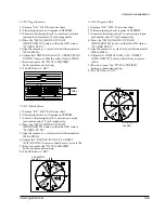
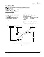
6. Auto white balance
1) Camera ÒE-EÓ, 3100¡K/5100¡K gray-scale chart.
2) Video(output) jack and AF MICOM.
4) Connect vectorscope input jack to video(output)
jack.
3) Press the ÒMENU (MODE UP)/DATE
(MODE DOWN)Ó button so that the OSD state is
ÒCF WBA XX XXÓ.
a. W/B Indoor
a-1. Aim the camera at a 3100¡K gray-scale chart
illuminated at 1500 to 2000 lx. (40us)
a-2. Press ÒTITLE (CONFIRM)Ó button so that
the white vector moves to the center on screen of
the vectorscope.
a-3. The OSD shows ÒOK!Ó.
b. W/B Outdoor
b-1. Aim the camera at a 5100¡K gray-scale chart
illuminated at 1500 to 2000 lx. (40us)
b-2. Press ÒTITLE (CONFIRM)Ó button so
that the white vector moves to the center on
screen of the vectorscope.
b-3. The OSD shows ÒOK!Ó.
Match the white luminance
point with the
black luminance
point
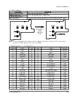
5. AUTO IRIS
1) Camera ÒE-EÓ, 3100¡K gray-scale chart.
2) Video(output) jack and AF MICOM.
3) Connect video(output) jack to waveform monitor
input jack and monitor TV jack respectively.
4) Press the ÒMENU (MODE UP)/DATE
(MODE DOWN)Ó button so that the OSD state is
ÒCE IRISA XX XXÓ.
5) Press ÒTITLE(confirm)Ó Button.
6) Then, the micro process will work;
- IRIS open, IRIS control minimum Value found.
- IRIS close, IRIS control minimum Value found.
- Store the data to mode 84 and mode 85.
7) The OSD shows ÒO.KÓ.
Center of
white level
100IRE
Optical
black level
H
40US
7. Pre white balance (I)
1) Camera ÒE-EÓ, 3100¡K gray-scale chart.
2) Video(output) jack and AF MICOM.
3) Connect vectorscope input jack to video(output)
jack.
4) Press the ÒMENU (MODE UP)/DATE
(MODE DOWN)Ó button so that the OSD state is
Ò1C CWBR XX XXÓ.
5) Aim the camera at a 3100¡K gray-scale chart
illuminated at 1500 to 2000 lx.
6) Adjust the Ò DISPLAY (DATA UP)/ C.RESET
(DATA DOWN)Ó button so that the white vector
moves to the B-Y axial on screen of the
vectorscope.
7) The OSD shows ÒOK!Ó.
Match the white luminance
point with the
black luminance
point
Summary of Contents for VP-L100
Page 7: ...Product Specifications 3 4 Samsung Electronics MEMO ...
Page 21: ...Disassembly and Reassembly 4 14 Samsung Electronics MEMO ...
Page 67: ...Exploded View and Parts List 6 2 Samsung Electronics 6 1 Cabinet Assembly 1 ...
Page 69: ...Exploded View and Parts List 6 4 Samsung Electronics 6 2 Cabinet Assembly 2 ...
Page 77: ...Exploded View and Parts List 6 12 Samsung Electronics 6 6 EVF ...
Page 79: ...Exploded View and Parts List 6 14 Samsung Electronics MEMO ...
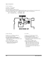
Page 105: ...Block Diagrams 8 2 Samsung Electronics 8 1 Overall Block Diagram Camera ...
Page 106: ...Block Diagrams Samsung Electronics 8 3 8 2 Overall Block Diagram VCR ...
Page 107: ...Block Diagrams 8 4 Samsung Electronics 8 3 DC DC Converter ...
Page 108: ...Block Diagrams Samsung Electronics 8 5 8 4 Drum Servo ...
Page 109: ...Block Diagrams 8 6 Samsung Electronics 8 5 Capstan Servo ...
Page 110: ...Block Diagrams Samsung Electronics 8 7 8 6 Video Playback SCL100 150 ...
Page 111: ...Block Diagrams 8 8 Samsung Electronics 8 7 Video Record SCL100 150 ...
Page 112: ...Block Diagrams Samsung Electronics 8 9 8 8 Video Playback VP L100 150 ...
Page 113: ...Block Diagrams 8 10 Samsung Electronics 8 9 Video Record VP L100 150 ...
Page 114: ...Block Diagrams Samsung Electronics 8 11 8 10 Audio ...
Page 115: ...Block Diagrams 8 12 Samsung Electronics 8 11 Camera Main ...
Page 117: ...PCB Diagrams 9 2 Samsung Electronics 9 1 Main Component Side ...
Page 118: ...PCB Diagrams Samsung Electronics 9 3 Conductor Side ...
Page 119: ...PCB Diagrams 9 4 Samsung Electronics 9 2 Rear Component Side Conductor Side ...
Page 120: ...PCB Diagrams Samsung Electronics 9 5 9 3 Function AE 9 4 Function VCR ...
Page 121: ...PCB Diagrams 9 6 Samsung Electronics 9 5 Function Menu ...
Page 123: ...PCB Diagrams 9 8 Samsung Electronics 9 7 CCD Component Side Conductor Side ...
Page 124: ...PCB Diagrams Samsung Electronics 9 9 9 8 LCD Component Side ...
Page 125: ...PCB Diagrams 9 10 Samsung Electronics Conductor Side ...
Page 126: ...PCB Diagrams Samsung Electronics 9 11 Component Side 9 1 MAIN BLUE ...
Page 127: ...PCB Diagrams 9 12 Samsung Electronics Conductor Side 9 1 MAIN BLUE ...
Page 128: ...Samsung Electronics 10 1 10 Wiring Diagram ...
Page 131: ...Schematic Diagrams Samsung Electronics 11 3 11 1 DC DC Converter ...
Page 132: ...Schematic Diagrams 11 4 Samsung Electronics T T T T T T 1 2 3 4 5 6 11 2 System Control Servo ...
Page 133: ...Schematic Diagrams Samsung Electronics 11 5 1 2 3 4 5 6 7 8 11 3 Video ...
Page 134: ...Schematic Diagrams 11 6 Samsung Electronics 11 4 Audio ...
Page 135: ...Schematic Diagrams Samsung Electronics 11 7 11 5 Front ...
Page 136: ...Schematic Diagrams 11 8 Samsung Electronics 11 6 Function AE ...
Page 137: ...Schematic Diagrams Samsung Electronics 11 9 11 7 Function VCR ...
Page 138: ...Schematic Diagrams 11 10 Samsung Electronics 11 8 Function MENU ...
Page 139: ...Schematic Diagrams Samsung Electronics 11 11 11 9 Rear ...
Page 140: ...Schematic Diagrams 11 12 Samsung Electronics 11 10 LCD ...
Page 141: ...Schematic Diagrams Samsung Electronics 11 13 11 11 CCD 1 2 3 4 5 6 7 8 ...
Page 142: ...Schematic Diagrams 11 14 Samsung Electronics 11 12 Camera Main 3 2 1 6 7 4 5 8 ...
Page 143: ...Schematic Diagrams Samsung Electronics 11 15 11 13 EVF ...
Page 144: ...Schematic Diagrams 11 16 Samsung Electronics 11 14 Adaptor ...


