background image

Level 3 Repair

Distribution, transmission, or infringement of any content or data from this document without Samsung’s written authorization is strictly prohibited.

Confidential and proprietary-the contents in this service guide subject to change without prior notice.

8-5

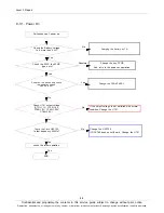
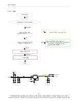
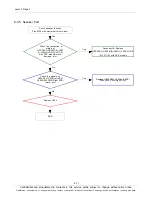
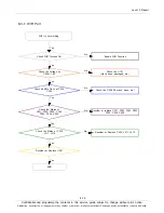
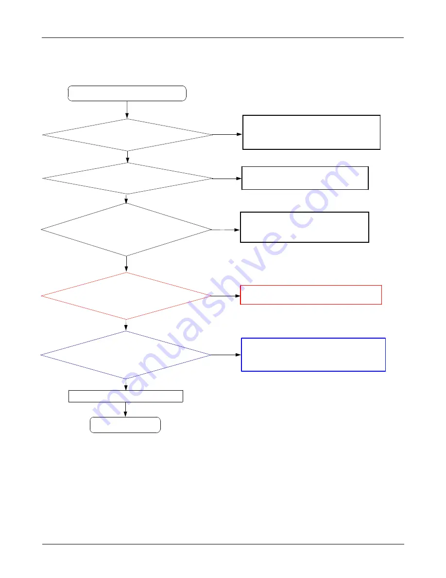
8-3-1. Power On

Check the PWR key-FPCB

(open, etc)

Cell-phone can`t power on.

Change the key

-

FPCB

And retry to the power-on operation.

END

No

Yes

Check U701 output voltage

(C731>1.1V, C732>1.0V,

C760>1.0V, C763>1.25V,

C764>2.0V,)

If the output voltage is not satisfied with normal

condition, Change the U701

No

Yes

No

Yes

Check the Battery Voltage.

Is it more than 3.4V?

Charging the battery by TA.

check the initial operation

Yes

Abnormal

Check the Clock OSC700

Is that frequency 32KHz?

Change the OSC700

If OSC700 does not still work, Change the U701

Yes

Change the FRONT ASSY

Power-on the phone and check

the power-on sound.

Sound is ok?

Yes

No

Summary of Contents for SM-T531

Page 1: ...tionality features specifications and other product information provided in this document including but not limited to benefits design pricing components performance availability and capabiliti es of the product are subject to change without notice Samsung reserves the right to alter this doc ument or the product described herein at anytime without obligation to provide notification of such change...

Page 2: ...is Service Manual is a property of Samsung Electronics Co Ltd Any unauthorized use of Manual can be punished under applicable International and or domestic law Samsung Electronics Co Ltd 2014 04 Rev 1 0 ⓒ ...

Page 3: ...33 DL 4357 4458 Tx Rx spacing 45MHz 45MHz 95MHz 80MHz 190MHz 80MHz 45MHz 45MHz Mod Bit rate Bit Period 270 833kbps 3 692us 270 833kbps 3 692us 270 833kbps 3 692us 270 833kbps 3 692us 3 84Mcps 3 84Mcps 3 84Mcps 3 84Mcps Time Slot Period Frame Period 576 9us 4 615ms 576 9us 4 615ms 576 9us 4 615ms 576 9us 4 615ms FrameLength 10ms Slotlength 0 667ms FrameLength 10ms Slotlength 0 667ms FrameLength 10m...

Page 4: ...3 dBm 17 9 3dBm 18 7 3 dBm 19 5 3 dBm TX Power control level EGSM900 5 33 2 dBm 6 31 2 dBm 7 29 2 dBm 8 27 2 dBm 9 25 2 dBm 10 23 2 dBm 11 21 2 dBm 12 19 2 dBm 13 17 2 dBm 14 15 2 dBm 15 13 2 dBm 16 11 3 dBm 17 9 3dBm 18 7 3 dBm 19 5 3 dBm TX Power control level DCS1800 0 30 3 dBm 1 28 3 dBm 2 26 3 dBm 3 24 3 dBm 4 22 3 dBm 5 20 3 dBm 6 18 3 dBm 7 16 3 dBm 8 14 3 dBm 9 12 4 dBm 10 10 4 dBm 11 8 4 ...

Page 5: ...infringement of any content or data from this document without Samsung s written authorization is strictly prohibited Main Function Android OS Kikat 4 4 2 Main 3 0 MP Sub 1 3 MP 10 1 WXGA TFT Full Touch C Type A GPS GLONASS BT v4 0 EDR with LE USB v2 0 Wi Fi 802 11 a b g n HT40 OTG Recording definition 1080p Sensors Accelerometer Hall IC Sensor Additional 1 2GHz Quad Core CPU ...

Page 6: ...vanced Audio Coding AVC Advanced Video Coding BER Bit Error Rate BPSK Binary Phase Shift Keying CA Conditional Access CDM Code Division Multiplexing C I Carrier to Interference DMB Digital Multimedia Broadcasting EN European Standard ES Elementary Stream ETSI European Telecommunications Standards Institute MPEG Moving Picture Experts Group PN Pseudo random Noise PS Pilot Symbol QPSK Quadrature Pha...

Page 7: ...h quality screwdrivers when servicing products Low quality screwdrivers can easily damage the heads of screws Use only conductor wire of the properly gauge and insulation for low resistance because of the low margin of error of most testing equipment We recommend 22 gauge twisted copper wire Hand soldering is not recommended because printed circuit boards PCBs can be easily damaged even with relat...

Page 8: ...static bags when you store or transport them Always use an anti static strap or wristband and remove electrostatic buildup or dissipate static electricity from your body before repairing ESDs Ensure that soldering irons have AC adapter with ground wires and that the ground wires are properly connected Use only desoldering tools with plastic tips to prevent static discharge Properly shield the work...

Page 9: ... prior notice Distribution transmission or infringement of any content or data from this document without Samsung s written authorization is strictly prohibited 6 1 S W Download 6 1 1 Pre requisite for S W Downloading Downloader Program Odin3 v3 09 3 exe SM T531 Data Link Cable GH39 01688A Binary files Settings ...

Page 10: ...ly prohibited Confidential and proprietary the contents in this service guide subject to change without prior notice 6 2 6 1 2 S W Downloader Program Load the binary download program by executing the Odin3 v3 09 3 exe Run this file 1 Option checking and select files Check Auto Reboot Re Partition and F Reset Time then select PIT BL AP and CSC File ...

Page 11: ...zation is strictly prohibited Confidential and proprietary the contents in this service guide subject to change without prior notice 6 3 2 Enter Device into Download Mode Press volume down button power key and Home Key at same time for 5 seconds then you can see below display Press volume up button to enter device into download mode ...

Page 12: ...ument without Samsung s written authorization is strictly prohibited Confidential and proprietary the contents in this service guide subject to change without prior notice 6 4 3 Connect the Device to PC via Data Cable Make sure ID COM box highlighted blue that the device is connected to the PC ...

Page 13: ...ed Confidential and proprietary the contents in this service guide subject to change without prior notice 6 5 4 Start Downloading PIT BL AP and CSC files by clicking Start button Then wait for PASS to be appear on the screen 5 Once the device boots up confirm the downloaded version name and etc 1234 Full Reset Apps Settings Backup and reset Factory data reset ...

Page 14: ...etary the contents in this service guide subject to change without prior notice Distribution transmission or infringement of any content or data from this document without Samsung s written authorization is strictly prohibited 4 1 Cellular phone Exploded View ...

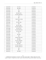
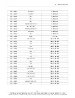
Page 15: ...ZD900 DIODE TVS 0406 001413 ZD502 DIODE TVS 0406 001494 ZD301 ZD302 ZD303 ZD304 DIODE TVS 0406 001494 ZD305 ZD610 DIODE TVS 0406 001505 D500 D501 ZD500 ZD501 DIODE TVS 0406 001549 ZD607 ZD608 ZD609 DIODE TVS 0406 001561 ZD602 DIODE TVS 0406 001606 ZD504 ZD505 ZD506 ZD507 DIODE TVS 0406 001606 ZD508 DIODE TVS 0505 002088 TR600 TR700 TR704 FET SILICON 0505 002341 Q900 TR703 FET SILICON 0505 002384 T...

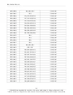
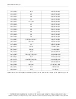
Page 16: ...NVERTER 1203 006182 U601 IC VOL DETECTOR 1203 006768 U801 IC DC DC CONVERTER 1203 006874 U800 IC MULTI REG 1203 007623 TR701 IC BATTERY ISOLATOR 1203 007834 U702 IC BATTERY 1203 007977 U802 IC SWITCH REG 1203 008057 U701 IC POWER SUPERVISOR 1203 008192 U600 IC VOL DETECTOR 1205 004548 U803 IC TRANSMITTER 1205 004803 U904 IC COMM CONTROLLER 1205 004825 U201 IC WIFI 1205 004829 U104 IC TRANSCEIVER 1...

Page 17: ...00162 R735 R736 R740 R741 R CHIP 2007 000162 R915 R CHIP 2007 000165 R732 R CHIP 2007 000166 R100 R CHIP 2007 000169 R101 R CHIP 2007 000170 R500 R501 R609 R616 R CHIP 2007 000170 R737 R CHIP 2007 000172 R502 R CHIP 2007 000566 R518 R CHIP 2007 000758 R301 R CHIP 2007 001284 R300 R CHIP 2007 001298 R508 R CHIP 2007 003015 R608 R906 R CHIP 2007 007107 R734 R CHIP 2007 007131 R913 R CHIP 2007 007137...

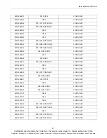
Page 18: ...P 2007 008354 R803 R CHIP 2007 008419 R918 R CHIP 2007 008420 R705 R CHIP 2007 008516 R319 R400 R440 R441 R CHIP 2007 008516 R445 R446 R459 R720 R CHIP 2007 008516 R911 R CHIP 2007 008588 R108 R109 R110 R111 R CHIP 2007 008588 R112 R407 R408 R456 R CHIP 2007 008588 R457 R617 R618 R CHIP 2007 008721 R802 R CHIP 2007 008774 R425 R614 R615 R905 R CHIP 2007 008774 R909 R CHIP 2007 008806 R103 R118 R50...

Page 19: ...41 C600 C CER CHIP 2203 000812 C601 C CER CHIP 2203 000854 C313 C812 C815 C CER CHIP 2203 001101 C620 C CER CHIP 2203 001153 C507 C510 C520 C CER CHIP 2203 001239 C501 C505 C506 C612 C CER CHIP 2203 002668 C102 C133 C170 C CER CHIP 2203 002687 C767 C769 C783 C784 C CER CHIP 2203 005056 C100 C104 C231 C CER CHIP 2203 005281 C117 C CER CHIP 2203 005288 C235 C814 C CER CHIP 2203 005552 C240 C CER CHI...

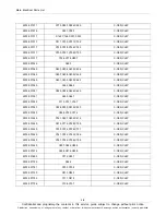
Page 20: ...C CER CHIP 2203 006048 C901 C902 C903 C904 C CER CHIP 2203 006194 C460 C CER CHIP 2203 006305 C312 C CER CHIP 2203 006348 C908 C CER CHIP 2203 006377 C766 C CER CHIP 2203 006399 C522 C523 C531 C CER CHIP 2203 006400 C200 C205 C CER CHIP 2203 006423 C300 C302 C400 C415 C CER CHIP 2203 006423 C416 C417 C418 C419 C CER CHIP 2203 006423 C420 C421 C423 C426 C CER CHIP 2203 006423 C427 C436 C438 C439 C ...

Page 21: ...19 C920 C921 C926 C CER CHIP 2203 006562 C927 C930 C931 C933 C CER CHIP 2203 006562 C934 C935 C939 C CER CHIP 2203 006647 C422 C CER CHIP 2203 006648 C435 C461 C CER CHIP 2203 006681 C306 C818 C909 C911 C CER CHIP 2203 006712 C607 C CER CHIP 2203 006824 C615 C CER CHIP 2203 006839 C180 C721 C800 C801 C CER CHIP 2203 006839 C804 C805 C806 C CER CHIP 2203 006841 C103 C109 C CER CHIP 2203 006844 C786...

Page 22: ...C405 C406 C CER CHIP 2203 007369 C407 C408 C409 C428 C CER CHIP 2203 007369 C431 C432 C433 C462 C CER CHIP 2203 007369 C464 C465 C CER CHIP 2203 007391 C225 C226 C424 C425 C CER CHIP 2203 007391 C455 C467 C CER CHIP 2203 007392 C113 C131 C167 C CER CHIP 2203 007393 C228 C230 C515 C530 C CER CHIP 2203 007393 C539 C723 C774 C CER CHIP 2203 007449 C161 C401 C402 C414 C CER CHIP 2203 007449 C512 C719 ...

Page 23: ...ER CHIP 2203 008312 C763 C764 C CER CHIP 2203 008394 C925 C CER CHIP 2404 001506 TA500 C TA CHIP 2703 001737 L101 L127 L138 INDUCTOR SMD 2703 002170 L129 INDUCTOR SMD 2703 002198 L135 INDUCTOR SMD 2703 002199 L120 INDUCTOR SMD 2703 002203 L130 L139 INDUCTOR SMD 2703 002204 L213 INDUCTOR SMD 2703 002207 L125 INDUCTOR SMD 2703 002208 L115 INDUCTOR SMD 2703 002267 L106 L107 L118 INDUCTOR SMD 2703 002...

Page 24: ...NDUCTOR SMD 2703 004289 L202 INDUCTOR SMD 2703 004530 L803 INDUCTOR SMD 2703 004599 L702 INDUCTOR SMD 2703 004599 L706 INDUCTOR SMD 2703 004697 L503 L504 L510 L511 INDUCTOR SMD 2703 004751 L700 L701 INDUCTOR SMD 2703 004764 L119 INDUCTOR SMD 2801 005154 OSC200 CRYSTAL SMD 2801 005300 OSC700 CRYSTAL SMD 2901 001625 F600 FILTER EMI ESD 2901 001690 C410 C411 C412 C413 FILTER EMI SMD 2901 001690 C457 ...

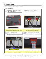
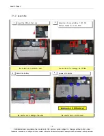
Page 25: ...quence when you disjoint Be careful not to damage the FPCBs Be careful not to damage the FPCBs Be careful not to damage the FPCBs 7 1 Disassembly and assembly Instructions 7 1 1 Disassembly Disengage the rear cover with the front cover by using the hook 1 Separate the 7 PIN I F connector TSP connector LCD connector from the PBA 2 3 Release the screw at 2 points Torque 1 1 0 1 kgf cm 4 1 2 3 4 blue...

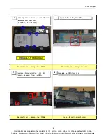
Page 26: ...uide subject to change without prior notice 7 2 Be careful not to damage the FPCBs Be careful not to damage the wires Be careful not to damage the FPCBs Be careful not to scratch cover Carefully release the screws at 6 different locations from the Front Torque 1 1 0 1 kgf cm 5 Separate the Battery from PBA 6 Separate all connector Key 1 3M 3M Camera Speaker from the PBA 7 Separate the PBA from Ass...

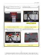
Page 27: ...ietary the contents in this service guide subject to change without prior notice 7 3 Be careful not to scratch cover Be careful not to damage the FPCBs Be careful not to damage the wires Be careful not to scratch cover 7 1 2 assemble Insert the PBA in the hook 1 Assemble all connector Key 1 3M 3M Camera Speaker to the PBA 2 Attach the battery 3 screws at 6 points 4 blue L1 5 6Points ...

Page 28: ...s in this service guide subject to change without prior notice 7 4 Be careful not to damage the FPCBs Be careful not to damage the FPCBs Be careful not to damage the FPCBs Follow the order Put the LCD FPCB and Close the black thin bar 6 screws at 2 Points 5 7 Insert the 7 PIN I F TSP LCD Connector and Close the black thin bar 8 Joint the Rear and the Front blue L1 5 2Point 7 PIN I F TSP LCD 1 2 3 ...

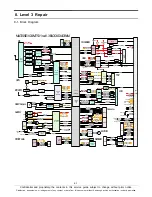
Page 29: ...W R LC D_S E LE C T LDO Filter TSPIC MXT1188S1 V P H_P W R TS P _LD O _O N LDO TS P _V DD_1 8V V P H_P W R TS P _LD O _O N LDO TS P _A V DD_2 8V V P H_P W R TS P _LD O _O N Booster RT8517G QW TS P _X V D D_9 1V TS P _S W 3_E N Y 0 42 X 0 24 TX 25 TX 26 R X 43 TS P _R S T TS PI2C TS P _nINT TA _nC O N NE C T TS P _V E ND O R TSP fromS M 5502 M U IC MOTOR ISA1200 M O TO RI2C V IB TO N E _P W M M O T...

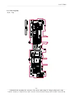
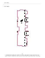
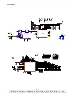
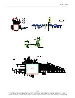
Page 30: ...ringement of any content or data from this document without Samsung s written authorization is strictly prohibited Confidential and proprietary the contents in this service guide subject to change without prior notice 8 2 8 2 PCB Diagrams 8 2 1 Top ...

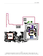
Page 31: ... or infringement of any content or data from this document without Samsung s written authorization is strictly prohibited Confidential and proprietary the contents in this service guide subject to change without prior notice 8 3 8 2 2 Bottom ...

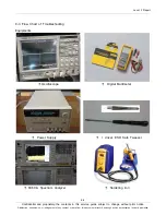
Page 32: ...msung s written authorization is strictly prohibited Confidential and proprietary the contents in this service guide subject to change without prior notice 8 4 8 3 Flow Chart of Troubleshooting Equipments Oscilloscope Digital Multimeter Power Supply driver ESD Safe Tweezer 8960 Spectrum Analyzer Soldering iron ...

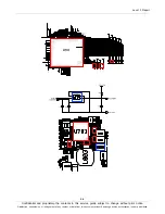
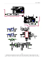
Page 33: ...e the key FPCB And retry to the power on operation END No Yes Check U701 output voltage C731 1 1V C732 1 0V C760 1 0V C763 1 25V C764 2 0V If the output voltage is not satisfied with normal condition Change the U701 No Yes No Yes Check the Battery Voltage Is it more than 3 4V Charging the battery by TA check the initial operation Yes Abnormal Check the Clock OSC700 Is that frequency 32KHz Change t...

Page 34: ...mission or infringement of any content or data from this document without Samsung s written authorization is strictly prohibited Confidential and proprietary the contents in this service guide subject to change without prior notice 8 6 ...

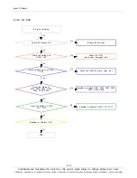
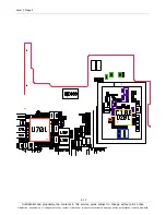
Page 35: ...hange without prior notice 8 7 8 3 2 Initial Initial Failure END Check the PMIC Reset PM_RESIN_N R619 H L or Yes Check the U701 crack open etc Check the oscillator clock waveforms 19 2MHz OSC700 C700 Check the OSC700 Crack open etc Check the output clock waveforms and frequency Test condition Oscilloscope setting 20 0ns div time division Abnormal Yes Normal No Re download SW the cell phone Change ...

Page 36: ...mission or infringement of any content or data from this document without Samsung s written authorization is strictly prohibited Confidential and proprietary the contents in this service guide subject to change without prior notice 8 8 ...

Page 37: ...rization is strictly prohibited Confidential and proprietary the contents in this service guide subject to change without prior notice 8 9 8 3 3 Charging Part TA USB Insert Yes END Charging Sequence Start V_BUS 4 5V No Check C766 C767 4 5V or may not connected TA USB Yes Battery is Charging No Resolder or Replace U702 or TR702 Yes ...

Page 38: ...TP_SLIMBUS_DATA EAR_MICBIAS_LDO_2 8V L509 C522 55 GND_SPKDRV NC 56 NC 57 6 BUCK_VOUT1 7 GND_BUCK 8 RESET_N 9 DMIC0_CLK 48 MIC_BIAS2 49 SPKR_DRVP 5 GND 50 SPKR_DRVM 51 MIC_BIAS3 52 MIC5_INP 53 MIC2_INM 54 MIC_BIAS1 40 GND_SPKDRV 41 MIC4_INM 42 MIC4_INP 43 MIC3_INM 44 MIC1_INP 45 VDD_SPKDRV 46 MIC5_INM 47 MIC2_INP 33 MODE 34 LDO_HI_CAP 35 VDD_VBAT 36 LINE_OUT1 37 MBHC_HSDET 38 MIC3_INP 39 MIC1_INM 4...

Page 39: ...rior notice 8 11 8 3 5 Speaker Part Check the signals on U505 R521 C524 Left SPK U506 R524 C534 Right SPK crack etc Check speaker function Play MP3 with maximum volume level No Replace U505 R521 C524 Left SPK U506 R524 C534 Right SPK END Yes Yes Check the connection status of HDC500 L HDC501 R L503 L L504 L L510 R L511 R with SPK module crack damage etc Yes No Reconnect Replace HDC500 L HDC501 R L...

Page 40: ...N 9 DMIC0_CLK U506 48 MIC_BIAS2 49 SPKR_DRVP 5 GND 50 SPKR_DRVM 51 MIC_BIAS3 52 MIC5_INP 53 MIC2_INM 54 MIC_BIAS1 40 GND_SPKDRV 41 MIC4_INM 42 MIC4_INP 43 MIC3_INM 44 MIC1_INP 45 VDD_SPKDRV 46 MIC5_INM 47 MIC2_INP 33 MODE 34 LDO_HI_CAP 35 VDD_VBAT 36 LINE_OUT1 37 MBHC_HSDET 38 MIC3_INP 39 MIC1_INM 4 INTR 26 EAROP 27 VDD_TX_RX 28 GND 29 MCLK 3 VDD_BUCK 30 SLIMBUS_DATA 31 EAROM 32 LINE_OUT2 19 VDD_D...

Page 41: ...ce 8 13 8 3 6 BT Part BT is not working Check BT function ON No Enable BT Function Yes END Check the Voltage on C226 1 8V No Check the U701 crack open damaged etc Yes Check 48MHz Clock at C238 C252 No Check the OSC200 crack open etc Yes Check the Status of C231 F203 F202 C233 F204 C236 C250 No Resolder or replace C231 F203 F202 C233 F204 C236 C250 Yes Resolder or Replace U201 Yes Yes Yes Check the...

Page 42: ...35 C789 VREG_L21_2P75 C788 C730 C709 VDD_GR4 VREG_S4_2P1 C757 BAT700 VREG_L26_1P25 C737 VDD_GR1 C752 VREG_L3_1P15 VDD_S5 C762 C707 C708 L702 C714 VREG_S4_2P1 98 GND GND 99 NC 90 NC 91 GND 92 VDD_S4 93 VOUT_LVS1 94 VREG_S4 95 BMS_CSN 96 USB_ID_IN 97 DNC 83 DNC 84 CBL_PWR_N 85 GND 86 GND 87 SLEEP_CLK1 88 NC 89 VDD_S1 9 VCOIN 76 PON_RESET_N 77 GND 78 79 VDD_GP VSW_S1 8 DNC 80 VSW_S4 81 NC 82 GND_S4 6...

Page 43: ...ission or infringement of any content or data from this document without Samsung s written authorization is strictly prohibited Confidential and proprietary the contents in this service guide subject to change without prior notice 8 15 ...

Page 44: ... 16 8 3 7 WIFI Part WIFI is not working Check WIFI function ON No Enable WIFI Function Yes END Check the Voltage on C226 1 8V No Check the U701 crack open damaged etc Yes Check 48MHz Clock at C238 C252 No Check the OSC200 crack open etc Yes Check the Status of C231 F203 F202 C233 F204 C236 C250 No Resolder or replace C231 F203 F202 C233 F204 C236 C250 Yes Resolder or Replace U201 Yes Yes Yes Check...

Page 45: ...35 C789 VREG_L21_2P75 C788 C730 C709 VDD_GR4 VREG_S4_2P1 C757 BAT700 VREG_L26_1P25 C737 VDD_GR1 C752 VREG_L3_1P15 VDD_S5 C762 C707 C708 L702 C714 VREG_S4_2P1 98 GND GND 99 NC 90 NC 91 GND 92 VDD_S4 93 VOUT_LVS1 94 VREG_S4 95 BMS_CSN 96 USB_ID_IN 97 DNC 83 DNC 84 CBL_PWR_N 85 GND 86 GND 87 SLEEP_CLK1 88 NC 89 VDD_S1 9 VCOIN 76 PON_RESET_N 77 GND 78 79 VDD_GP VSW_S1 8 DNC 80 VSW_S4 81 NC 82 GND_S4 6...

Page 46: ...ission or infringement of any content or data from this document without Samsung s written authorization is strictly prohibited Confidential and proprietary the contents in this service guide subject to change without prior notice 8 18 ...

Page 47: ...nction Yes END Check the Voltage on R107 1 3V R106 2 0V C161 1 8V No Check the U701 crack open damaged etc Yes Check 19 2MHz Clock at C171 No Check the U701 crack open etc Yes Check the Voltage of VDD_FEM GPS_2 75V at L200 No Resolder or change the U200 Yes Check the Status of L203 C203 F201 L202 L201 F200 L206 C202 C201 No Resolder or Replace L203 C203 F201 L202 L201 F200 L206 C202 C201 Yes Yes Y...

Page 48: ...EG_L20 56 VREG_S2 GND_S2 43 VREG_L15 44 BB_CLK1_EN 45 VSW_S2 46 VSW_S2 47 VDD_S3 48 VDD_L25 49 VREG_L14 5 XTAL_19M_IN VSW_S3 VREG_S3 36 37 VREG_L4 38 VREG_L10 39 RF_CLK2 4 VDD_GR1 40 NC 41 VDD_GR7 42 BB_CLK2 NC VREG_L19 29 3 VREG_L2 30 VREG_L17 31 BB_CLK1 32 VREG_L18 33 GND_S1 34 VDD_S2 35 VREG_S1 21 VSW_S1 GND_S1 22 23 GND_S3 24 VREG_L26 25 VREG_L5 26 NC 27 VDD_GR4 28 17 GND_XO 170 VPRE_BYP 171 O...

Page 49: ...ission or infringement of any content or data from this document without Samsung s written authorization is strictly prohibited Confidential and proprietary the contents in this service guide subject to change without prior notice 8 21 ...

Page 50: ...is still off after PWR ON Yes No Check the connection of SLC800 Yes Check the voltage of L804 3 3V Yes Check the C812 and High 20V Yes Yes No No Check the Backlight Driver IC U802 or Replace the L802L803 C811 D800 C813 C814 Check the Buck Booster U801 or Replace U801 Reconnect the SLC800 Check the voltage of C808 3 3V C809 1 8V Check or Replace the LDO U800 C808 C809 Check the L800 C801 and High 1...

Page 51: ...RXCM G4 DSRXD2M DSRXD3M G5 E4 E5 VDD_LVDS1_33 LVTX1DP E6 E7 LVTX1DN F1 DSRXD0P F2 DSRXD1P F3 DSRXCP DSRXD2P F4 D3 D4 VDD_MIPI VSS_LVDS1_33 D5 D6 LVTX1CP LVTX1CN D7 E1 VDDIO VSSIO E2 E3 VSS_MIPI VDD_MIPI C2 C3 GPIO2 GPIO1 C4 C5 VSS_LVDS1_12 LVTX1BP C6 C7 LVTX1BN I2C_SCL D1 D2 GPIO4 VSS_MIPI B1 B2 VDDC VSSC B3 B4 TM VDD_LVDS1_12 B5 B6 LVTX1AP LVTX1AN B7 C1 I2C_SDA GPIO3 2 NC A1 VSSIO VDDIO A2 A3 RES...

Page 52: ...ission or infringement of any content or data from this document without Samsung s written authorization is strictly prohibited Confidential and proprietary the contents in this service guide subject to change without prior notice 8 24 ...

Page 53: ...D Replace U904 Yes Yes Check the Voltage R903 R904 TSP I2C Signal Resolder or Replace R903 R904 No Yes No Check the Voltage on C937 8 2V Resolder or Replace U905 R912 R913 ZD900 C908 C909 C910 C911 C915 Touch Screen does not work Yes Check TSP Connector on Main PBA Reconnect the SLC900 Check the Voltage on C932 2 8V Resolder or Replace U903 L901 C931 C932 C900 C901 C902 C903 C904 Check the Voltage...

Page 54: ...2 X15 N13 X14 M11 CHRG_IN M12 X13 M13 X12 M2 NC M3 NC M4 GND M5 VDD M6 VDD L4 VDD L5 USBDP_5 DBG_CLK L6 USBDM_1 DBG_DATA L7 VDD_INPUT L8 XIN L9 CHG_2 M1 NC M10 RESERVED K3 X23 L1 X26 L10 COMMSEL L11 X11 L12 X10 L13 XVDD L2 XVDD L3 NC J13 X5 J2 X21 J3 GND K1 GND K11 X9 K12 X8 K13 GND K2 X24 H2 X19 H3 X18 H6 RESERVED H7 RESERVED H8 ADDSEL_5 J1 X22 J11 X7 J12 X6 G2 XVDD G3 X16 G6 X25 G8 GND H1 X20 H1...

Page 55: ...ission or infringement of any content or data from this document without Samsung s written authorization is strictly prohibited Confidential and proprietary the contents in this service guide subject to change without prior notice 8 27 ...

Page 56: ...to change without prior notice 8 28 8 3 11 3M CAM Yes Check the Camera connector on Main PBA Reconnect the HDC900 No Check the voltage C916 1 25V C917 C927 2 8V C918 1 8V Resolder C916 C917 C918 C927 U902 Resolder C752 C754 or Replace the PBA No Yes END Replace the camera module Camera function does not work Yes Yes Check R905 C925 C940 Resolder R905 C925 C940 or Replace the PBA No Yes Check F901 ...

Page 57: ...6 150m A L16 L23 600m A L4 50m A 2000m A Def ault O n VREG _L24_1P3 L701 C 76 0 C 74 3 C 76 4 C 74 9 C 73 6 VREG _L19_2P85 C 73 1 VREG _L18_2P95 C 73 2 C 76 3 C 73 5 C 78 9 VREG _L21_2P75 C 78 8 C 73 0 C 75 7 VREG _L26_1P25 C 73 7 C 75 2 C 76 2 L702 VREG_S4_2 P1 N C 90 N C 91 VREG _S4 95 DN C 83 DN C 84 N C 89 VS W_S1 8 DN C 80 VS W_S4 81 N C 82 G ND _S 4 69 VREG _L25 70 G ND _X O _B U FF 62 G ND ...

Page 58: ...ission or infringement of any content or data from this document without Samsung s written authorization is strictly prohibited Confidential and proprietary the contents in this service guide subject to change without prior notice 8 30 ...

Page 59: ...ange without prior notice 8 31 8 3 12 1 3M CAM Yes Check the Camera connector on Main PBA Reconnect the HDC801 No Check the voltage C933 1 8V C934 2 8V C935 C920 1 8V No Yes END Replace the camera module Camera function does not work Yes Resolder C933 C934 C935 C920 U900 Resolder C752 C754 or Replace the PBA Abnormal Check R909 C928 C941 Yes Resolder R909 C928 C941 or Replace the PBA No Check F900...

Page 60: ...C 40 VREG_L15 43 VSW_S2 45 VREG_L18 32 GND_S1 33 VSW_S3 35 36 VREG_S3 VREG_L10 38 NC 26 NC 28 29 VREG_L19 VREG_L17 30 VREG_L17 18 VREG_L16 19 VREG_S1 20 VSW_S1 21 22 GND_S1 GND_S3 23 VREG_L26 24 165 GND_XO 17 VREG_L11 16 GND_CHG_HP 150 GND_CHG_HP 153 NC 145 NC 147 GND_WLED VREG_L13 14 GND_CHG 142 NC 133 VREG_L27 127 VREG_L9 128 VREG_L7 GND_REF 117 118 VREG_L8 VREG_L24 12 GND 109 110 GND_OVP GND 11...

Page 61: ...ission or infringement of any content or data from this document without Samsung s written authorization is strictly prohibited Confidential and proprietary the contents in this service guide subject to change without prior notice 8 33 ...

Page 62: ... s written authorization is strictly prohibited Confidential and proprietary the contents in this service guide subject to change without prior notice 8 34 8 3 13 OTG OTG does not work Yes No Check the U600 Check if V_BUS goes 5V C617 Yes END Yes Check the V_BUS_5V goes 5V C777 No Check the U703 Yes Replace IF FPCB ...

Page 63: ...26 26 27 27 28 28 29 29 3 3 16 16 17 17 18 18 19 19 2 2 20 20 21 21 22 22 1 1 10 10 11 11 12 12 13 13 14 14 15 15 V_BUS_5V SLC600 ZD610 I O 1 2 I O I O 3 I O 4 F600 GND 5 GND 6 MAIN_MICBIAS_2 8V R613 R615 C610 R614 C612 R606 ZD606 L602 C615 R610 C620 R604 R607 ZD607 MIC_N_CON MUIC_DM MUIC_DP JTAG_USB_ID MUIC_ID OVP_E MIC_P_CON HOME_KEY R731 R727 VREG_L6_1P8 VPH_PWR C775 VPH_PWR C778 TP_USB_HS_DM R...

Page 64: ...5dBm 8 3 14 GSM850 WCDMA Band5 RX CONTINUO US RX ON RF INPUT 4408CH AMP 50dBm NORMAL CONDITION catch the channel Check the Voltage at C105 VOUT_CHARGER Check component soldering status OK at U104 CHECK soldered L104 C108 RFS100 Resolder or change PAM100 C105 Resolder or change U104 Check L130 65dBm Resolder or change Check L130 WCDMA Band5 GSM 850 Receiver is O K Resolder or change U401 1 END NO Y...

Page 65: ...O 17 TX_BB_QP 18 VDD_RF2_R_BB 19 2 TX_BB_IP VDD_RF1_LNA 20 VDD_RF1_G_PLL 21 PDET_RFFB_IN 22 TX_BB_QM 23 DAC_REF 1 RX_LB2_IN 10 GNSS_RF_IN 11 TX_BB_IM 12 RF_ON 13 GND 14 GND 15 VDD_RF2_T_DA 16 GND U104 TX2_OUT C129 L101 C182 R117 SHORT C117 L104 C130 L106 L100 C162 SHORT R107 L116 C140 R116 C177 5 VMODE GND 6 7 GND CPL_OUT 8 9 GND 13 GND RFOUTHB 14 15 CPLIN GND 16 17 GND RFIN 2 3 VENHB VENLB 4 PAM1...

Page 66: ...5dBm 8 3 15 GSM900 WCDMA Band8 RX CONTINUO US RX ON RF INPUT 4408CH AMP 50dBm NORMAL CONDITION catch the channel Check the Voltage at C105 VOUT_CHARGER Check component soldering status OK at U104 CHECK soldered L104 C108 RFS100 Resolder or change PAM100 C105 Resolder or change U104 Check L120 65dBm Resolder or change Check L120 WCDMA Band5 GSM 850 Receiver is O K Resolder or change U401 1 END NO Y...

Page 67: ...O 17 TX_BB_QP 18 VDD_RF2_R_BB 19 2 TX_BB_IP VDD_RF1_LNA 20 VDD_RF1_G_PLL 21 PDET_RFFB_IN 22 TX_BB_QM 23 DAC_REF 1 RX_LB2_IN 10 GNSS_RF_IN 11 TX_BB_IM 12 RF_ON 13 GND 14 GND 15 VDD_RF2_T_DA 16 GND U104 TX2_OUT C129 L101 C182 R117 SHORT C117 L104 C130 L106 L100 C162 SHORT R107 L116 C140 R116 C177 5 VMODE GND 6 7 GND CPL_OUT 8 9 GND 13 GND RFOUTHB 14 15 CPLIN GND 16 17 GND RFIN 2 3 VENHB VENLB 4 PAM1...

Page 68: ... 65dBm 8 3 16 GSM1900 GSM1800 RX CONTINUO US RX ON RF INPUT 4408CH AMP 50dBm NORMAL CONDITION catch the channel Check the Voltage at C105 VOUT_CHARGER Check component soldering status OK at U104 CHECK soldered L104 C108 RFS100 Resolder or change PAM100 C105 Resolder or change U104 Check L106 65dBm Resolder or change Check L106 WCDMA Band5 GSM 850 Receiver is O K Resolder or change U401 1 END NO YE...

Page 69: ...O 17 TX_BB_QP 18 VDD_RF2_R_BB 19 2 TX_BB_IP VDD_RF1_LNA 20 VDD_RF1_G_PLL 21 PDET_RFFB_IN 22 TX_BB_QM 23 DAC_REF 1 RX_LB2_IN 10 GNSS_RF_IN 11 TX_BB_IM 12 RF_ON 13 GND 14 GND 15 VDD_RF2_T_DA 16 GND U104 TX2_OUT C129 L101 C182 R117 SHORT C117 L104 C130 L106 L100 C162 SHORT R107 L116 C140 R116 C177 5 VMODE GND 6 7 GND CPL_OUT 8 9 GND 13 GND RFOUTHB 14 15 CPLIN GND 16 17 GND RFIN 2 3 VENHB VENLB 4 PAM1...

Page 70: ...8 65dBm 8 3 17 WCDMA BAND 1 RX CONTINUO US RX ON RF INPUT 4408CH AMP 50dBm NORMAL CONDITION catch the channel Check the Voltage at C105 VOUT_CHARGER Check component soldering status OK at U104 CHECK soldered L104 C108 RFS100 Resolder or change PAM100 C105 Resolder or change U104 Check L116 65dBm Resolder or change Check L116 WCDMA Band5 GSM 850 Receiver is O K Resolder or change U401 1 END NO YES ...

Page 71: ...O 17 TX_BB_QP 18 VDD_RF2_R_BB 19 2 TX_BB_IP VDD_RF1_LNA 20 VDD_RF1_G_PLL 21 PDET_RFFB_IN 22 TX_BB_QM 23 DAC_REF 1 RX_LB2_IN 10 GNSS_RF_IN 11 TX_BB_IM 12 RF_ON 13 GND 14 GND 15 VDD_RF2_T_DA 16 GND U104 TX2_OUT C129 L101 C182 R117 SHORT C117 L104 C130 L106 L100 C162 SHORT R107 L116 C140 R116 C177 5 VMODE GND 6 7 GND CPL_OUT 8 9 GND 13 GND RFOUTHB 14 15 CPLIN GND 16 17 GND RFIN 2 3 VENHB VENLB 4 PAM1...

Page 72: ...8 65dBm 8 3 18 WCDMA BAND 2 RX CONTINUO US RX ON RF INPUT 4408CH AMP 50dBm NORMAL CONDITION catch the channel Check the Voltage at C105 VOUT_CHARGER Check component soldering status OK at U104 CHECK soldered L104 C108 RFS100 Resolder or change PAM100 C105 Resolder or change U104 Check L116 65dBm Resolder or change Check L127 WCDMA Band5 GSM 850 Receiver is O K Resolder or change U401 1 END NO YES ...

Page 73: ...O 17 TX_BB_QP 18 VDD_RF2_R_BB 19 2 TX_BB_IP VDD_RF1_LNA 20 VDD_RF1_G_PLL 21 PDET_RFFB_IN 22 TX_BB_QM 23 DAC_REF 1 RX_LB2_IN 10 GNSS_RF_IN 11 TX_BB_IM 12 RF_ON 13 GND 14 GND 15 VDD_RF2_T_DA 16 GND U104 TX2_OUT C129 L101 C182 R117 SHORT C117 L104 C130 L106 L100 C162 SHORT R107 L116 C140 R116 C177 5 VMODE GND 6 7 GND CPL_OUT 8 9 GND 13 GND RFOUTHB 14 15 CPLIN GND 16 17 GND RFIN 2 3 VENHB VENLB 4 PAM1...

Page 74: ...46 8 3 19 WCDMA BAND 1 TX CONTINUO US RX ON RF INPUT 4408CH AMP 50dBm PAM100 PIN 15 About 30dBm Check the Voltage at C105 VOUT_CHARGER Check component soldering status OK at PAM101 CHECK soldered L104 C108 RFS100 Resolder or change PAM100 C105 Resolder or change PAM101 Check L127 30dBm Resolder or change Check C129 WCDMA Band5 GSM 850 Receiver is O K Resolder or change U401 1 END YES NO NO YES NO ...

Page 75: ...O 17 TX_BB_QP 18 VDD_RF2_R_BB 19 2 TX_BB_IP VDD_RF1_LNA 20 VDD_RF1_G_PLL 21 PDET_RFFB_IN 22 TX_BB_QM 23 DAC_REF 1 RX_LB2_IN 10 GNSS_RF_IN 11 TX_BB_IM 12 RF_ON 13 GND 14 GND 15 VDD_RF2_T_DA 16 GND U104 TX2_OUT C129 L101 C182 R117 SHORT C117 L104 C130 L106 L100 C162 SHORT R107 L116 C140 R116 C177 5 VMODE GND 6 7 GND CPL_OUT 8 9 GND 13 GND RFOUTHB 14 15 CPLIN GND 16 17 GND RFIN 2 3 VENHB VENLB 4 PAM1...

Page 76: ...48 8 3 20 WCDMA BAND 2 TX CONTINUO US RX ON RF INPUT 4408CH AMP 50dBm PAM100 PIN 15 About 30dBm Check the Voltage at C105 VOUT_CHARGER Check component soldering status OK at PAM102 CHECK soldered L104 C108 RFS100 Resolder or change PAM100 C105 Resolder or change PAM102 Check L127 30dBm Resolder or change Check L124 WCDMA Band5 GSM 850 Receiver is O K Resolder or change U401 1 END YES NO NO YES NO ...

Page 77: ...O 17 TX_BB_QP 18 VDD_RF2_R_BB 19 2 TX_BB_IP VDD_RF1_LNA 20 VDD_RF1_G_PLL 21 PDET_RFFB_IN 22 TX_BB_QM 23 DAC_REF 1 RX_LB2_IN 10 GNSS_RF_IN 11 TX_BB_IM 12 RF_ON 13 GND 14 GND 15 VDD_RF2_T_DA 16 GND U104 TX2_OUT C129 L101 C182 R117 SHORT C117 L104 C130 L106 L100 C162 SHORT R107 L116 C140 R116 C177 5 VMODE GND 6 7 GND CPL_OUT 8 9 GND 13 GND RFOUTHB 14 15 CPLIN GND 16 17 GND RFIN 2 3 VENHB VENLB 4 PAM1...

Page 78: ...8 3 21 GSM850 WCDMA BAND 5 TX CONTINUO US RX ON RF INPUT 4408CH AMP 50dBm PAM100 PIN 15 About 30dBm Check the Voltage at C105 VOUT_CHARGER Check component soldering status OK at PAM102 CHECK soldered L104 C108 RFS100 Resolder or change PAM100 C105 Resolder or change PAM102 Check L127 30dBm Resolder or change Check L131 WCDMA Band5 GSM 850 Receiver is O K Resolder or change U401 1 END YES NO NO YES...

Page 79: ...O 17 TX_BB_QP 18 VDD_RF2_R_BB 19 2 TX_BB_IP VDD_RF1_LNA 20 VDD_RF1_G_PLL 21 PDET_RFFB_IN 22 TX_BB_QM 23 DAC_REF 1 RX_LB2_IN 10 GNSS_RF_IN 11 TX_BB_IM 12 RF_ON 13 GND 14 GND 15 VDD_RF2_T_DA 16 GND U104 TX2_OUT C129 L101 C182 R117 SHORT C117 L104 C130 L106 L100 C162 SHORT R107 L116 C140 R116 C177 5 VMODE GND 6 7 GND CPL_OUT 8 9 GND 13 GND RFOUTHB 14 15 CPLIN GND 16 17 GND RFIN 2 3 VENHB VENLB 4 PAM1...

Page 80: ...8 3 22 GSM900 WCDMA BAND 8 TX CONTINUO US RX ON RF INPUT 4408CH AMP 50dBm PAM100 PIN 15 About 30dBm Check the Voltage at C105 VOUT_CHARGER Check component soldering status OK at PAM101 CHECK soldered L104 C108 RFS100 Resolder or change PAM100 C105 Resolder or change PAM101 Check L127 30dBm Resolder or change Check C141 WCDMA Band5 GSM 850 Receiver is O K Resolder or change U401 1 END YES NO NO YES...

Page 81: ...O 17 TX_BB_QP 18 VDD_RF2_R_BB 19 2 TX_BB_IP VDD_RF1_LNA 20 VDD_RF1_G_PLL 21 PDET_RFFB_IN 22 TX_BB_QM 23 DAC_REF 1 RX_LB2_IN 10 GNSS_RF_IN 11 TX_BB_IM 12 RF_ON 13 GND 14 GND 15 VDD_RF2_T_DA 16 GND U104 TX2_OUT C129 L101 C182 R117 SHORT C117 L104 C130 L106 L100 C162 SHORT R107 L116 C140 R116 C177 5 VMODE GND 6 7 GND CPL_OUT 8 9 GND 13 GND RFOUTHB 14 15 CPLIN GND 16 17 GND RFIN 2 3 VENHB VENLB 4 PAM1...

Reviews: