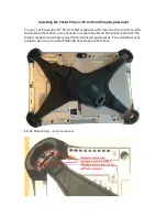
background image

8. Level 3 Repair

8-1

Confidential and proprietary-the contents in this service guide subject to change without prior notice.

Distribution, transmission, or infringement of any content or data from this document without Samsung’s written authorization is strictly prohibited.

8-1. Block Diagram

V_BUS_5V

VREG_L6_1P8

VREG_L17_2P95

EMMC_DATA[ 0:7]

EMMC_CLK

EMMC_CMD

MSM_RESOUT

Micr oSD

VREG_L6_1P8

VREG_L18_2P95

T_FLASH_D([ 0:3] )

T_FLASH_CLK

T_FLASH_CMD

T_FLASH_DETECT

MATI SSE WI FI  SM-T530 rev0.4 BLOCK DI AGRAM

VREG_L6_1P8

VREG_S4_2P1

VREG_L4_1P2

CODEC_RESET_N

SLI MBUS

SLI MBUS_CLK, SLI MBUS_DATA

VPH_PWR

PMIC_AUDI O_REF_CLK

from PM8226, PMI C

CODEC_I NT_N

EAR_VPS_L / R

Analog Sw it ch

FSA2270

EAR_L /  R_CRADLE_CON

EAROUT_L /  R

LINEOUT_ON

3.5ø

Ear  Jack

EAR_G_DET

EAR_L_DET

1.353V

DET_3.5

(Active Low)

SPK_L /  R

AMP

YDA16 8

AMP

YDA16 8

VPH_PWR


EAR_MIC-

EAR_MIC_P /  N

EAR_ADC

EAR_SEND_END

0.77V

(Active Low)

MAIN_MICBI AS_2.8V

MAIN_MI C_P /  N

Main MIC

Speaker

AUDIO

to SM5502, MUI C

-

+

-

+

VREG_L6_1P8

VREG_L24_1P3

VREG_L16_3P0

VREG_L10_1P8

BT/ WI FI

DI PLEXER

KEY_ANT

WL_RFIO_5G

Band Pass

Filt er

WLAN_SET
WLAN_CLK

WLAN_DATA[ 0:2]

WLAN_I / Q

Bluetooth SBI

BT_WIFI _CLK_IN

BT_WIFI_CLK_OUT

OSC

DI PLEXER

HI GH

HIGH

LOW

LOW

BT_SSBI , BT_DATA, BT_CTL

WI FI 2.4GHz

WIFI  5GHz

GPS_ANT

WTR_GNSS_P/ M

LNA

RDALN16

SAW

Filt er

VDD_FEM/ GPS_2P75

GPS

SAW

Filt er

3M_CLK_P /  N

Fil t er

3M_DP /  N

CAM_ANALOG_EN

VPH_PWR

3M_MCLK

CAM I2C

3M_nRST

3M_nSTBY

VTCAM_EN

VPH_PWR

VTCAM_MCLK

VT_CAM_CLK_P / N

VT_CAM_DP /  N

CAM I2C

VT_CAM_nRST

VT_CAM_nSTBY

VREG_L28_1P8

CAM_AVDD_2.8V

VREG_L26_1P225

VTCAM_CORE_1.8V

Filt er

CAM I 2C

VREG_L28_1P8

VT CAM

3M CAM

LDO

LDO

SI M
car d

VREG_L6_1P8

VREG_L22_3P0

UIM1_RESET

UIM1_CLK

UI M1_DATA

UI M1_DETECT

ADJ_DET_D

GRIP_1P8

GRI P Sensor

SX9500I ULTRT

RF_TOUCH

RF_TOUCH_AP

ANT_COM

GRI P Sensor I2C

Main

ANT

LDO

VREG_L15_2P8

ADJ_DET

GRI P Sensor

EAR_ADC

to PM8226
       PMIC

STORTAGE

AP

MSM8926

LCD

TSP

Camera

MOTOR

SENSOR

CHARGER

USB

MI PI LVDS

Tr ansm it t er

TC358764

VREG_L5_1P2

LVDS_3V3
LVDS_1V8

VPH_PWR

LVDS_LDO_EN

LCD_CLK_P / N

LCD_D[ 0:3] _P / N

LVDS I2C

LVDS_RX_0P /  N_F

Filt er

LVDS_RST

LVDS_CLK_P /  N_F

LVDS_RX_1P /  N_F
LVDS_RX_2P /  N_F
LVDS_RX_3P /  N_F

Filt er

3.3V BUCK

TPS630 10

VPH_PWR

DI SPLAY_3.3V

LCD_EN

Backlight

Dr iver

LM855 8

LED_BACKLI GHT_RESET

BACKLIGHT_PWM_AP

LED_BACKLI GHT I 2C

LED_VOUT_18V

LED_K([ 1:4] )

VPH_PWR

LCD_SELECT

LDO

Filt er

TSP I C

MXT1188S1

VPH_PWR

TSP_LDO_ON

LDO

TSP_VDD_1.8V

VPH_PWR

TSP_LDO_ON

LDO

TSP_AVDD_2.8V

VPH_PWR

TSP_LDO_ON

Boost er

RT8517GQW

TSP_XVDD_9.1V

TSP_SW3_EN

Y[ 0:42]

X[ 0:24]

TX25
TX26

RX43

TSP_RST

TSP I2C

TSP_nINT

TA_nCONNECT

TSP_VENDOR

TSP

from SM5502, MUIC

MOTOR

I SA1200

MOTOR I 2C

VIBTONE_PWM

MOT_EN

MOTOR_P
MOTOR_N

VREG_L6_1P8

M

VPH_PWR

ACC Sensor

K2HH

VREG_L19_2P85
VREG_LVS1_1P8

SENSOR I 2C

ACC_I NT

HALL I C

VREG_L6_1P8

DETECT_FLI PCOVER

Side Key

Hom e Key 

WARM RESET

FT8010MPX

MSM_RES_IN

VREG_L6_1P8

VREG_L19_2P85

PM_KYPD_PWR_N

PM_RESIN_N

VOL_UP

VOL_DOWN

MSM_RES_IN

HOME_KEY

VREG_S3_1P35

VREG_S3_2P1

VREG_S1_1P15
VREG_S2_1P05

AP

MSM8926

to WCD9306

CODEC

VREG_L[ 1:28]

VREF_LPDDR2

PMIC_AUDI O_REF_CLK

BAT_UIM_ALARM

GRFC(12)

VREF_MSM_PX_MPP1

VREF_LDO_MPP3

PA_THERM0_MPP5

EAR_ADC

BBCLK_MSM

BBCLK_MSM_EN

MSM_PS_HOLD

RFCLK1_19.2M

SLEEP_CLK

to WCD9306, CODEC

to WTR2605, Transceiver

from Ear Jack

from Thermistor for PA

Thermistor AP

AP_THERM

Thermistor SYSTEM

SYS_THERM

XO_THERM

19.2M_IN

19.2M_OUT

OSC

to All System

Micr o USB 

Sw it ch I C

SM5502

VREG_L6_1P8

V_BUS_5V

VPH_PWR

MUIC_DP /  DM

MUI C_ID

Fi lt er

VBUS_IN

OVP

MUI C I2C

MUIC_INT_N

PMIC_JI GONB

I F_CON_SENSE

MSM_UART_RX / TX

USB_HS_DP /  DM

OTG_I D

EAR_L / R_CRADLE_CON

IF_VOUT_CHATGER

BATT_ID

TA_INT

CHG I2C

TA_nCHG

VOUT_CHARGER

VREG_L6_1P8

TA_ENABLE

VPH_PWR

(Root)

VOUT_CHARGER

(Root)

IF_VOUT_CHATGER

Sw it ch 

BMS_SENSE_P /  N

IF_CON_SENSE

(CHGOUT)

(USBI N)

(FETDRV)

(VSYS)

CHARGER

SMB358

Bat t er y

Sw it ch 

to PM8226, PMI C

CBL_PWR_N

from FSA2270

               Analog Switch

UART_BOOT_ON

TA_nCONNECT

(EN)

AP

MSM8926

for LDOs

(USBI N)

V_BUS_5V

VPH_PWR

(VPH_PWR, VDD_x)

VOUT_CHARGER

(VBAT, VBAT_SNS)

Micr o

USB
CON 

16GB

eMMC

PMI C

PM8926

Audio CODEC

WCD9306

Bluet oot h

WI FI

WCN3660A

AP /  CP

MSM8926

LCD

POP RAM

LPDDR3

1.5G

WCSS_XO

GPS

WGR7640

VREG_L1_1P225

VREG_L10_1P8

CH0_SSBI _TX_GPS

GPS_BB_RX_IM/ I P

GPS_BB_RX_QM/ QP

RFCLK1_19.2M

from PM8226, PMI C

Summary of Contents for SM-T530/NU

Page 1: ...tionality features specifications and other product information provided in this document including but not limited to benefits design pricing components performance availability and capabiliti es of...

Page 2: ...is Service Manual is a property of Samsung Electronics Co Ltd Any unauthorized use of Manual can be punished under applicable International and or domestic law Samsung Electronics Co Ltd 2014 03 Rev 1...

Page 3: ...quality screwdrivers when servicing products Low quality screwdrivers can easily damage the heads of screws Use only conductor wire of the properly gauge and insulation for low resistance because of...

Page 4: ...tatic bags when you store or transport them Always use an anti static strap or wristband and remove electrostatic buildup or dissipate static electricity from your body before repairing ESDs Ensure th...

Page 5: ...the contents in this service guide subject to change without prior notice Distribution transmission or infringement of any content or data from this document without Samsung s written authorization is...

Page 6: ...or infringement of any content or data from this document without Samsung s written authorization is strictly prohibited Main Function Android OS Kikat 4 4 2 Main 3 0 MP Sub 1 3 MP 10 1 WXGA TFT Full...

Page 7: ...tary the contents in this service guide subject to change without prior notice Distribution transmission or infringement of any content or data from this document without Samsung s written authorizati...

Page 8: ...0406 001361 ZD300 DIODE TVS 0406 001390 ZD900 DIODE TVS 0406 001413 ZD502 DIODE TVS 0406 001505 D500 D501 ZD500 DIODE TVS 0406 001505 ZD501 DIODE TVS 0406 001549 ZD607 ZD608 ZD609 DIODE TVS 0406 0015...

Page 9: ...TR701 IC BATTERY ISOLATOR 1203 007834 U702 IC BATTERY 1203 007977 U802 IC SWITCH REG 1203 008057 U701 IC POWER SUPERVISOR 1203 008192 U600 IC VOL DETECTOR 1205 004548 U803 IC TRANSMITTER 1205 004803 U...

Page 10: ...007107 R734 R CHIP 2007 007131 R913 R CHIP 2007 007137 R510 R CHIP 2007 007142 R724 R916 R CHIP 2007 007315 R417 R CHIP 2007 007316 R901 R907 R CHIP 2007 007317 R521 R522 R524 R525 R CHIP 2007 007318...

Page 11: ...CHIP 2007 009920 R442 R443 R449 R CHIP 2007 010856 R728 R CHIP 2007 011043 R421 R CHIP 2203 000254 C803 C938 C CER CHIP 2203 000278 C252 C CER CHIP 2203 000330 C238 C CER CHIP 2203 000386 C508 C509 C5...

Page 12: ...4 C609 C802 C CER CHIP 2203 006048 C901 C902 C903 C904 C CER CHIP 2203 006305 C325 C CER CHIP 2203 006348 C908 C CER CHIP 2203 006377 C766 C CER CHIP 2203 006399 C522 C523 C531 C CER CHIP 2203 006400...

Page 13: ...P 2203 006681 C818 C909 C911 C CER CHIP 2203 006712 C607 C CER CHIP 2203 006824 C615 C CER CHIP 2203 006839 C721 C800 C801 C804 C CER CHIP 2203 006839 C805 C806 C CER CHIP 2203 006841 C239 C242 C CER...

Page 14: ...203 007449 C409 C414 C428 C431 C CER CHIP 2203 007449 C432 C433 C434 C462 C CER CHIP 2203 007449 C464 C465 C512 C719 C CER CHIP 2203 007449 C728 C729 C733 C734 C CER CHIP 2203 007449 C736 C737 C741 C7...

Page 15: ...4030 L206 INDUCTOR SMD 2703 004086 L201 INDUCTOR SMD 2703 004127 L703 INDUCTOR SMD 2703 004289 L202 INDUCTOR SMD 2703 004530 L803 INDUCTOR SMD 2703 004599 L702 L706 INDUCTOR SMD 2703 004697 L503 L504...

Page 16: ...PC FFC PIC 3709 001811 CD300 CONNECTOR CARD EDGE 3711 006925 HDC900 HDC901 HEADER BOARD TO BOARD 3711 007173 HDC400 HDC500 HEADER BOARD TO BOARD 3711 008010 HDC501 HDC600 HEADER BOARD TO BOARD 3711 00...

Page 17: ...rior notice Distribution transmission or infringement of any content or data from this document without Samsung s written authorization is strictly prohibited 6 1 S W Download 6 1 1 Pre requisite for...

Page 18: ...y prohibited Confidential and proprietary the contents in this service guide subject to change without prior notice 6 2 6 1 2 S W Downloader Program Load the binary download program by executing the O...

Page 19: ...ation is strictly prohibited Confidential and proprietary the contents in this service guide subject to change without prior notice 6 3 2 Enter Device into Download Mode Press volume down button power...

Page 20: ...ment without Samsung s written authorization is strictly prohibited Confidential and proprietary the contents in this service guide subject to change without prior notice 6 4 3 Connect the Device to P...

Page 21: ...d Confidential and proprietary the contents in this service guide subject to change without prior notice 6 5 4 Start Downloading PIT BL AP and CSC files by clicking Start button Then wait for PASS to...

Page 22: ...uence when you disjoint Be careful not to damage the FPCBs Be careful not to damage the FPCBs Be careful not to damage the FPCBs 7 1 Disassembly and assembly Instructions 7 1 1 Disassembly Disengage t...

Page 23: ...ide subject to change without prior notice 7 2 Be careful not to damage the FPCBs Be careful not to damage the wires Be careful not to damage the FPCBs Be careful not to scratch cover Carefully releas...

Page 24: ...etary the contents in this service guide subject to change without prior notice 7 3 Be careful not to scratch cover Be careful not to damage the FPCBs Be careful not to damage the wires Be careful not...

Page 25: ...in this service guide subject to change without prior notice 7 4 Be careful not to damage the FPCBs Be careful not to damage the FPCBs Be careful not to damage the FPCBs Follow the order Put the LCD...

Page 26: ...N LCD_CLK_P N LCD_D 0 3 _P N LVDS I2C LVDS_RX_0P N_F Filt er LVDS_RST LVDS_CLK_P N_F LVDS_RX_1P N_F LVDS_RX_2P N_F LVDS_RX_3P N_F Filt er 3 3V BUCK TPS63010 VPH_PWR DISPLAY_3 3V LCD_EN Backlight Drive...

Page 27: ...ingement of any content or data from this document without Samsung s written authorization is strictly prohibited Confidential and proprietary the contents in this service guide subject to change with...

Page 28: ...or infringement of any content or data from this document without Samsung s written authorization is strictly prohibited Confidential and proprietary the contents in this service guide subject to chan...

Page 29: ...sung s written authorization is strictly prohibited Confidential and proprietary the contents in this service guide subject to change without prior notice 8 4 8 3 Flow Chart of Troubleshooting Equipme...

Page 30: ...the key FPCB And retry to the power on operation END No Yes Check U701 output voltage C731 1 1V C732 1 0V C760 1 0V C763 1 25V C764 2 0V If the output voltage is not satisfied with normal condition C...

Page 31: ...ission or infringement of any content or data from this document without Samsung s written authorization is strictly prohibited Confidential and proprietary the contents in this service guide subject...

Page 32: ...ange without prior notice 8 7 8 3 2 Initial Initial Failure END Check the PMIC Reset PM_RESIN_N R619 H L or Yes Check the U701 crack open etc Check the oscillator clock waveforms 19 2MHz OSC700 C700 C...

Page 33: ...ission or infringement of any content or data from this document without Samsung s written authorization is strictly prohibited Confidential and proprietary the contents in this service guide subject...

Page 34: ...ization is strictly prohibited Confidential and proprietary the contents in this service guide subject to change without prior notice 8 9 8 3 3 Charging Part TA USB Insert Yes END Charging Sequence St...

Page 35: ...P_SLIMBUS_DATA EAR_MICBIAS_LDO_2 8V L509 C522 55 GND_SPKDRV NC 56 NC 57 6 BUCK_VOUT1 7 GND_BUCK 8 RESET_N 9 DMIC0_CLK 48 MIC_BIAS2 49 SPKR_DRVP 5 GND 50 SPKR_DRVM 51 MIC_BIAS3 52 MIC5_INP 53 MIC2_INM...

Page 36: ...ior notice 8 11 8 3 5 Speaker Part Check the signals on U505 R521 C524 Left SPK U506 R524 C534 Right SPK crack etc Check speaker function Play MP3 with maximum volume level No Replace U505 R521 C524 L...

Page 37: ...9 DMIC0_CLK U506 48 MIC_BIAS2 49 SPKR_DRVP 5 GND 50 SPKR_DRVM 51 MIC_BIAS3 52 MIC5_INP 53 MIC2_INM 54 MIC_BIAS1 40 GND_SPKDRV 41 MIC4_INM 42 MIC4_INP 43 MIC3_INM 44 MIC1_INP 45 VDD_SPKDRV 46 MIC5_INM...

Page 38: ...e 8 13 8 3 6 BT Part BT is not working Check BT function ON No Enable BT Function Yes END Check the Voltage on C226 1 8V No Check the U701 crack open damaged etc Yes Check 48MHz Clock at C238 C252 No...

Page 39: ...5 C789 VREG_L21_2P75 C788 C730 C709 VDD_GR4 VREG_S4_2P1 C757 BAT700 VREG_L26_1P25 C737 VDD_GR1 C752 VREG_L3_1P15 VDD_S5 C762 C707 C708 L702 C714 VREG_S4_2P1 98 GND GND 99 NC 90 NC 91 GND 92 VDD_S4 93...

Page 40: ...ssion or infringement of any content or data from this document without Samsung s written authorization is strictly prohibited Confidential and proprietary the contents in this service guide subject t...

Page 41: ...16 8 3 7 WIFI Part WIFI is not working Check WIFI function ON No Enable WIFI Function Yes END Check the Voltage on C226 1 8V No Check the U701 crack open damaged etc Yes Check 48MHz Clock at C238 C252...

Page 42: ...5 C789 VREG_L21_2P75 C788 C730 C709 VDD_GR4 VREG_S4_2P1 C757 BAT700 VREG_L26_1P25 C737 VDD_GR1 C752 VREG_L3_1P15 VDD_S5 C762 C707 C708 L702 C714 VREG_S4_2P1 98 GND GND 99 NC 90 NC 91 GND 92 VDD_S4 93...

Page 43: ...ssion or infringement of any content or data from this document without Samsung s written authorization is strictly prohibited Confidential and proprietary the contents in this service guide subject t...

Page 44: ...ND Check the Voltage on C243 1 8V C240 1 225V No Check the U701 crack open damaged etc Yes Check 19 2MHz Clock at C246 No Check the U701 crack open etc Yes Check the Voltage of VDD_FEM GPS_2 75V at L2...

Page 45: ...S2 56 57 GND_S2 VSW_S2 58 VDD_GR5 59 XTAL_19M_OUT 6 VDD_GR5 60 VSW_S2 46 VDD_S3 47 VDD_L25 48 VREG_L14 49 XTAL_19M_IN 5 VREG_L28 50 VREG_L23 51 VREG_L22 52 VDD_GR1 4 NC 40 VDD_GR7 41 BB_CLK2 42 VREG_L...

Page 46: ...ssion or infringement of any content or data from this document without Samsung s written authorization is strictly prohibited Confidential and proprietary the contents in this service guide subject t...

Page 47: ...s still off after PWR ON Yes No Check the connection of SLC800 Yes Check the voltage of L804 3 3V Yes Check the C812 and High 20V Yes Yes No No Check the Backlight Driver IC U802 or Replace the L802L8...

Page 48: ...XCM G4 DSRXD2M DSRXD3M G5 E4 E5 VDD_LVDS1_33 LVTX1DP E6 E7 LVTX1DN F1 DSRXD0P F2 DSRXD1P F3 DSRXCP DSRXD2P F4 D3 D4 VDD_MIPI VSS_LVDS1_33 D5 D6 LVTX1CP LVTX1CN D7 E1 VDDIO VSSIO E2 E3 VSS_MIPI VDD_MIP...

Page 49: ...ssion or infringement of any content or data from this document without Samsung s written authorization is strictly prohibited Confidential and proprietary the contents in this service guide subject t...

Page 50: ...Replace U904 Yes Yes Check the Voltage R903 R904 TSP I2C Signal Resolder or Replace R903 R904 No Yes No Check the Voltage on C937 8 2V Resolder or Replace U905 R912 R913 ZD900 C908 C909 C910 C911 C91...

Page 51: ...X15 N13 X14 M11 CHRG_IN M12 X13 M13 X12 M2 NC M3 NC M4 GND M5 VDD M6 VDD L4 VDD L5 USBDP_5 DBG_CLK L6 USBDM_1 DBG_DATA L7 VDD_INPUT L8 XIN L9 CHG_2 M1 NC M10 RESERVED K3 X23 L1 X26 L10 COMMSEL L11 X1...

Page 52: ...ssion or infringement of any content or data from this document without Samsung s written authorization is strictly prohibited Confidential and proprietary the contents in this service guide subject t...

Page 53: ...o change without prior notice 8 28 8 3 11 3M CAM Yes Check the Camera connector on Main PBA Reconnect the HDC900 No Check the voltage C916 1 25V C917 C927 2 8V C918 1 8V Resolder C916 C917 C918 C927 U...

Page 54: ...CK L18 1 1 L 9 L L20 VDD_GR3 4 6 4MHz L9 1200mA L16 6 4MHz L19 L19 L6 L11 L22 L5 LVS L13 L2 L26 150mA L16 L23 600mA L4 50mA 2000mA Default On VREG_L24_1P3 L701 C760 C743 C764 C749 C736 VREG_L19_2P85 C...

Page 55: ...ssion or infringement of any content or data from this document without Samsung s written authorization is strictly prohibited Confidential and proprietary the contents in this service guide subject t...

Page 56: ...nge without prior notice 8 31 8 3 12 1 3M CAM Yes Check the Camera connector on Main PBA Reconnect the HDC801 No Check the voltage C933 1 8V C934 2 8V C935 C920 1 8V No Yes END Replace the camera modu...

Page 57: ...40 VREG_L15 43 VSW_S2 45 VREG_L18 32 GND_S1 33 VSW_S3 35 36 VREG_S3 VREG_L10 38 NC 26 NC 28 29 VREG_L19 VREG_L17 30 VREG_L17 18 VREG_L16 19 VREG_S1 20 VSW_S1 21 22 GND_S1 GND_S3 23 VREG_L26 24 165 GN...

Page 58: ...ssion or infringement of any content or data from this document without Samsung s written authorization is strictly prohibited Confidential and proprietary the contents in this service guide subject t...

Page 59: ...s written authorization is strictly prohibited Confidential and proprietary the contents in this service guide subject to change without prior notice 8 34 8 3 13 OTG OTG does not work Yes No Check the...

Page 60: ...6 26 27 27 28 28 29 29 3 3 16 16 17 17 18 18 19 19 2 2 20 20 21 21 22 22 1 1 10 10 11 11 12 12 13 13 14 14 15 15 V_BUS_5V SLC600 ZD610 I O 1 2 I O I O 3 I O 4 F600 GND 5 GND 6 MAIN_MICBIAS_2 8V R613 R...

Page 61: ...anced Audio Coding AVC Advanced Video Coding BER Bit Error Rate BPSK Binary Phase Shift Keying CA Conditional Access CDM Code Division Multiplexing C I Carrier to Interference DMB Digital Multimedia B...

Reviews: