background image

SAMSUNG Proprietary-Contents may change without notice

Main Electrical Parts List

2-10

This Document can not be used without Samsung's authorization

9

10

11

12

1

2

3

<pic 1>

<pic 2>

1) Insert the pwr-key.

2) Insert the volume-key.

caution

1) Be careful for the direction of vol-key, pwr-key

1) Insert the 3*4key FPCB to the CONNECTOR

along the SILK LINE.

2) Put the green TAPE on the connector.

caution

1) vol-key, pwr-key FPCB must be covered with

REAR COVER plastic.

2) Be careful not to give demage to locker.

1) Put the pwr-key like the picture below.

2) Put the motor like the picture below.

Wires must be in order like the picture
below.(blue wire: top, red wire: bottom)

caution

1) Wires must be in order.

1) Insert the 3*4key FPCB to the CONNECTOR

along the SILK LINE.

2) Put the green TAPE on the connector.

caution

1) Check the connection of FPCB.
2) Be careful for the scratch and crack of FPCB.

Summary of Contents for SGH-M600

Page 1: ...ONE CONTENTS 1 Specification 2 Exploded View and Parts List 3 Flow Chart of Troubleshooting 4 Array course control 5 Block Diagrams 6 PCB Diagrams 7 MAIN Electrical Parts List 8 Reference data 9 Safet...

Page 2: ...1 Power ON 9 1 3 1 2 Initial 9 4 3 1 3 Sim Part 9 6 3 1 4 Charging Part 9 8 3 1 5 Microphone Part 9 9 3 1 6 Speaker Part 9 11 3 1 7 LCD 9 13 3 1 8 Camera 9 16 3 2 RF 3 2 1 GSM Receiver 3 18 3 2 2 DCS...

Page 3: ...ectrical Parts List 6 Block Diagrams 7 PCB Diagrams 8 Reference data 9 Safety Precautions 9 1 Repair Precaution 9 1 9 2 ESD Electrostatically Sensitive Devices Precaution 9 2 10 Product Function 10 1...

Page 4: ...Rx spacing 45 MHz 45 MHz 95 MHz Mod Bit rate Bit Period 270 833 Kbps 3 692 us 270 833 Kbps 3 692 us 270 833 Kbps 3 692 us Time Slot Period Frame Period 576 9 us 4 615 ms 576 9 us 4 615 ms 576 9 us 4...

Page 5: ...10 23 2 dBm 11 21 2 dBm 12 19 2 dBm 13 17 2 dBm 14 15 2 dBm 15 13 2 dBm 16 11 3 dBm 17 9 3 dBm 18 7 3 dBm 19 5 3 dBm TX Power control level DCS1800 0 30 3 dBm 1 28 3 dBm 2 26 3 dBm 3 24 3 dBm 4 22 3...

Page 6: ...ot be used without Samsung s authorization 2 1 Cellular phone Exploded View QFU01 QCK01 QIF01 QBA01 QKP02 QCA01 QSP01 QLC01 QME02 QFL01 QSC01 QCR05 QMO01 QVK01 QMP01 QAN02 QMI03 QME01 QBR04 QKP01 QVO0...

Page 7: ...SUB XEF DSA GH98 04443A QLC01 ELA UNIT SGH_M600 LCD MODULE GH96 02764A QME02 DOME SHEET DOME SHEET 9 KEY GH59 04438A QMO01 MOTOR DC SGH M600 GH31 00340A QMP01 PBA MAIN SGHM600 GH92 03632A QPC01 MEA FP...

Page 8: ...GH44 01702A EARPHONE B TYPE GH59 04557A LABEL P UNIT SEAL GH68 00518B MANUAL SFC GH68 04336A LABEL R WATER SOAK GH68 09361A MANUAL USERS EU RUSSIAN GH68 15270A LABEL R MAIN SER GH68 15468B BOX P UNIT...

Page 9: ...SAMSUNG Proprietary Contents may change without notice Main Electrical Parts List 2 4 This Document can not be used without Samsung s authorization...

Page 10: ...of 2 points 2 Disjoint the key pad FPCB from connector 3 Take off the motor from the FRONT plastic using tweezers and disjoint pwr key FPCB volume key FPCB from the FRONT plastic caution 1 Be careful...

Page 11: ...stic caution 1 Be careful for the FPCB s crack 1 Disjoint the key pad bracket from the FRONT plastic 2 Remove the Key pad rubber caution 1 Be careful for scratch 7 8 1 Slide up like the picture below...

Page 12: ...uthorization 9 10 1 Lift up the LCD PBA slightly Remove the camera module 2 Disjoint the speaker caution 1 Be careful for the demage of camera speaker 11 Pic 1 1 Slide up like the picture below 2 Disj...

Page 13: ...ic 3 Push 1 2 in numerical order caution 1 Be careful for the scratch and crack of FPCB 2 Be careful for the demage of LCD 1 Joint the 4 screws in numerical order caution 1 Be careful for scratch 2 4...

Page 14: ...T 2 Put the MIC and bracket like the picture below caution 1 Check the flatness of MIC 1 Fold the FPCB like the picture below 2 Joint the FPCB connector caution 1 Check the connection of FPCB 7 1 Fold...

Page 15: ...ILK LINE 2 Put the green TAPE on the connector caution 1 vol key pwr key FPCB must be covered with REAR COVER plastic 2 Be careful not to give demage to locker 1 Put the pwr key like the picture below...

Page 16: ...ts may change without notice Main Electrical Parts List 2 11 This Document can not be used without Samsung s authorization 1 Joint the 5 screws of REAR COVER plastic 2 Joint the RF cover caution 1 Be...

Page 17: ...V Check UCP300 and C317 Pin A13 and pin A14 2 8V Check UCP300 and C318 Freq 26MHz Vrms 300mV Vpp 900mV Check the clock generation circuit related to OSC100 Check the initial operation END No Yes Yes Y...

Page 18: ...SAMSUNG Proprietary Contents may change without notice Flow Chart of Troubleshooting 3 2 This Document can not be used without Samsung s authorization...

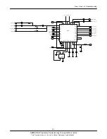
Page 19: ...V I D X N E X 32 E D O M X 25 8 XOUT 31 1 L A T X RFIPN 18 RFIPP 17 H O F R 16 15 L O F R SCLK 1 SDIO 3 D D V 12 D D V 13 C N 35 36 NC RFIAN 24 RFIAP 23 RFIDN 20 RFIDP 19 RFIEN 22 RFIEP 21 27 C F A 6...

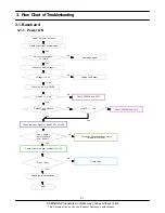
Page 20: ...UCP300 if it has some problem it is to be replaced Yes No Is the pin K9 of UCP300 Low High Yes No Check the UCP300 if it has some problem it is to be replaced There is 32 768kHz wave forms at the C237...

Page 21: ...ROMEN A6 XCP_D0 XCP_A17 XCP_A18 K14 L14 XCP_A19 E14 XCP_A2 L15 XCP_A20 L16 XCP_A21 XCP_A3 D15 XCP_A4 B15 C14 XCP_A1 F11 XCP_A10 D16 F14 XCP_A11 G14 XCP_A12 XCP_A13 G13 G17 XCP_A14 XCP_A15 J12 XCP_A16...

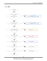
Page 22: ...e voltage at pin 1 of CN301 2 8V Insert SIM is displayed on the LCD Check the SIM connector s CN301 connection to SIM card Check the UCP300 Resolder or change CN301 END No Yes Yes Yes Yes No No Is the...

Page 23: ...SAMSUNG Proprietary Contents may change without notice Flow Chart of Troubleshooting 3 7 This Document can not be used without Samsung s authorization...

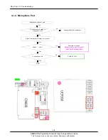
Page 24: ...Samsung s authorization 3 1 4 Microphone Part Is the assembled status of microphone O K Microphone does not work Reassembled the microphone Resolder or change R415 R417 C412 C411 C414 C415 R425 R421 R...

Page 25: ...without notice Flow Chart of Troubleshooting 3 9 This Document can not be used without Samsung s authorization C412 VCCA_2 9V C411 VR401 R424 C415 R423 C414 R421 VR400 R417 R425 R420 R415 MIC_P MIC_N...

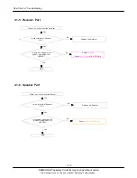
Page 26: ...e is no sound from the Receiver Is the terminal of Receiver O K No Replace the Receiver Yes No Yes Check UCP300 Check V103 V104 LCD PCB Part Is there any signals at the pin P11 and pin N12 of UCP300 E...

Page 27: ...SAMSUNG Proprietary Contents may change without notice Flow Chart of Troubleshooting 3 11 This Document can not be used without Samsung s authorization...

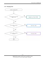
Page 28: ...SAMSUNG Proprietary Contents may change without notice Flow Chart of Troubleshooting 3 12 This Document can not be used without Samsung s authorization 3 1 7 Charging Part...

Page 29: ...SAMSUNG Proprietary Contents may change without notice Flow Chart of Troubleshooting 3 13 This Document can not be used without Samsung s authorization...

Page 30: ...SAMSUNG Proprietary Contents may change without notice Flow Chart of Troubleshooting 3 14 This Document can not be used without Samsung s authorization...

Page 31: ...0dBm NORMAL CONDITION catch the channel CHECK ANT contact U100 pin 13 2 8V PAM100 CHECK pin16 65dBm U100 CHECK pin21 22 65dBm PAM100 RFS100 resolder or change PAM100 resolder or change C103 C108 L100...

Page 32: ...0dBm YES NORMAL CONDITION catch the channel CHECK ANT contact U100 pin 13 2 8V PAM100 CHECK pin18 65dBm U100 CHECK pin19 20 65dBm PAM100 RFS100 resolder or change PAM100 resolder or change C111 C113 L...

Page 33: ...0dBm YES NORMAL CONDITION catch the channel CHECK ANT contact U100 pin 13 2 8V PAM100 CHECK pin20 65dBm U100 CHECK pin17 18 65dBm PAM100 RFS100 resolder or change PAM100 resolder or change C111 C113 L...

Page 34: ...PAM100 pin6 2 8 V PAM100 pin12 about 2 3 dBm NO NO UCP300 check change YES YES C109 RFS100 check change PAM100 pin7 3 7 V BATTERY check change NO PAM100 pin 8 1 6V YES NO R109 Check YES PAM100 pin11...

Page 35: ...20dB UCP300 check change PAM100 pin6 2 8 V PAM100 pin12 about 2 3 dBm NO NO YES YES C109 RFS100 check change PAM100 pin7 3 7 V BATTERY check change NO YES R109 Check PAM100 pin 8 1 6V NO YES NO PAM100...

Page 36: ...6 V I D X N E X 32 E D O M X 25 8 XOUT 31 1 L A T X RFIPN 18 RFIPP 17 H O F R 16 15 L O F R SCLK 1 SDIO 3 D D V 12 D D V 13 C N 35 36 NC RFIAN 24 RFIAP 23 RFIDN 20 RFIDP 19 RFIEN 22 RFIEP 21 27 C F A...

Page 37: ...X T V 6 8 1 3 X R 6 1 4 X R 4 1 V1 2 T T A B V 7 1 S B V 4 2 S B V 5 VCC1 0 1 1 GND1 13 GND2 15 GND3 17 GND4 19 GND5 21 N I X T 0 0 9 0 5 8 M S G 1 1 0 2 1 X R 2 X R PAM100 2 1 T N A N I S C P S C D...

Page 38: ...SAMSUNG Proprietary Contents may change without notice Flow Chart of Troubleshooting 3 22 This Document can not be used without Samsung s authorization...

Page 39: ...SAMSUNG Proprietary Contents may change without notice 4 Array course control 4 2 This Document can not be used without Samsung s authorization...

Page 40: ...ument can not be used without Samsung s authorization Software Downloading 4 1 Downloading Binary Files Three binary files for downloading M600 M600XXYY s3 Main source code binary 4 2 Pre requsite for...

Page 41: ...thout Samsung s authorization 4 3 S W Downloader Program 1 Load the binary download program by executing the Optiflash exe 2 Select the Options Settings Generic Specify hardware platform Choose hardwa...

Page 42: ...msung s authorization 3 Select the COM port when the download cable is connected Additionally you can select the maximum transfer speed OptiFlash will use to communicate with the phone However OptiFla...

Page 43: ...used without Samsung s authorization 4 Select the Flash Verify Browse Set the directory path and choose the lastet s w binary for example M600XXYY s3 for the downloader binary setting Make sure that...

Page 44: ...g Flash button push the button and END at the same time Then press Flash Downloader will upload the binary file as below for the downloading 6 When downloading is finished successfully there is a All...

Page 45: ...SAMSUNG Proprietary Contents may change without notice 5 Block Diagrams 5 1 This Document can not be used without Samsung s authorization...

Page 46: ...SAMSUNG Proprietary Contents may change without notice 5 Block Diagrams 5 2 This Document can not be used without Samsung s authorization...

Page 47: ...6 PCB Diagrams 6 1 CONFIDENTIAL Service Schematics...

Page 48: ...PCB Diagrams 6 2 CONFIDENTIAL Service Schematics...

Page 49: ...18 RX2 16 PAM100 1 DCS PCSIN 13 ANT109 SGHF310 ANT 1 2 VBAT R106 R103 L102 C129 25V 6 3V C122 VCCD_2 9V L103 L100 25V C108 R108 R105 6 3V C105 6 3V C123 C120 C103 25V 25V C110 C121 6 3V L101 C111 6 3...

Page 50: ...L1 K4 XPA21 CP_SCK J6 XPA23 PWM2 H6 XPA0 CS1N M15 N2 XPA10 IRQ4 K5 XPA11 IRDARX XPA12 IRDATX N1 G6 G3 XPA15 TX0 H4 XPA16 RX0 L3 N3 D7 XCP_TCK D13 XCP_TDO XCP_TMS G8 XCP_TRSTN F9 C13 XCP_WEN F4 XOSC32O...

Page 51: ...F9 GNDS4 F10 GNDS5 G7 G8 G3 DB7 G4 F4 DB8 DB9 F1 DINTR P3 GNDB F6 GNDD M10 GNDQ E8 GNDS1 F7 GNDS10 H7 H8 GNDS11 K2 DB10 F2 DB11 F3 DB12 E2 DB13 E3 DB14 D3 DB15 D2 DB2 K3 J5 DB3 DB4 J6 DB5 H5 DB6 CH_BD...

Page 52: ...VCCA_2 9V R401 R413 C410 C405 VR400 C406 R406 AVLC5S01100 C407 R414 C422 R431 C423 C412 6 3V C418 VCCA_2 9V C417 C411 6 3V PGND 1 PVDD 5 PVSS 6 SGND SVDD 9 13 SVDD 11 SVSS _SHDN 16 INL 14 INL INR 7 I...

Page 53: ...VDD_CORE0 G5 VDD_IO1 G6 GND_CORE0 G7 GND_CORE1 F1 PHD6 F10 PLCD10 F2 PHD5 F3 PHD7 F4 GND_IO1 F7 VDD_IO2 F8 PGPIO9 F9 PLCD8 E1 PHD0 E10 PLCD11 E2 PHD2 E3 PHD1 VDD_PLL E4 E7 VDD_CORE1 E8 PLCD9 E9 PLCD13...

Page 54: ...33 33 34 34 35 35 36 36 37 37 38 38 24 24 25 25 26 26 27 27 28 28 29 29 3 3 30 30 17 17 18 18 19 19 2 2 20 20 21 21 22 22 23 23 1 1 10 10 11 11 12 12 13 13 14 14 15 15 16 16 FPC600 C607 C608 VBAT C61...

Page 55: ...PCB Diagrams 6 3 CONFIDENTIAL Service Schematics...

Page 56: ...IPLEX SA 1009 001020 U201 IC HALL EFFECT S W SA 1108 000111 UME200 IC MCP SA 1201 002180 U400 IC AUDIO AMP SA 1201 002278 PAM100 IC POWER AMP SA 1203 003304 UCP300 IC POWER SUPERVISOR SA 1203 003663 U...

Page 57: ...160 R210 R CHIP SA 2007 000161 R405 R CHIP SA 2007 000161 R411 R CHIP SA 2007 000162 R206 R CHIP SA 2007 000162 R301 R CHIP SA 2007 000162 R307 R CHIP SA 2007 000170 R215 R CHIP SA 2007 000171 R105 R...

Page 58: ...483 R504 R CHIP SA 2007 008483 R601 R CHIP SA 2007 008516 R108 R CHIP SA 2007 008516 R109 R CHIP SA 2007 008531 R200 R CHIP SA 2007 008531 R201 R CHIP SA 2007 008531 R600 R CHIP SA 2007 008542 L101 R...

Page 59: ...0812 C302 C CER CHIP SA 2203 000812 C405 C CER CHIP SA 2203 000812 C406 C CER CHIP SA 2203 000812 C416 C CER CHIP SA 2203 000812 C418 C CER CHIP SA 2203 000940 C304 C CER CHIP SA 2203 000995 C220 C CE...

Page 60: ...6048 C211 C CER CHIP SA 2203 006048 C215 C CER CHIP SA 2203 006048 C225 C CER CHIP SA 2203 006048 C226 C CER CHIP SA 2203 006048 C227 C CER CHIP SA 2203 006048 C228 C CER CHIP SA 2203 006048 C229 C CE...

Page 61: ...6423 C122 C CER CHIP SA 2203 006423 C123 C CER CHIP SA 2203 006423 C219 C CER CHIP SA 2203 006423 C414 C CER CHIP SA 2203 006423 C415 C CER CHIP SA 2203 006423 C500 C CER CHIP SA 2203 006423 C503 C CE...

Page 62: ...06562 C501 C CER CHIP SA 2203 006562 C502 C CER CHIP SA 2203 006562 C510 C CER CHIP SA 2203 006562 C601 C CER CHIP SA 2203 006626 C401 C CER CHIP SA 2203 006626 C404 C CER CHIP SA 2203 006648 C118 C C...

Page 63: ...004587 OSC100 CRYSTAL SMD SA 2904 001592 F100 FILTER SAW SA 2904 001599 F101 FILTER SAW SA 2904 001600 F102 FILTER SAW SA 3301 001342 L200 BEAD SMD SA 3301 001729 L501 BEAD SMD SA 3301 001729 L502 BE...

Page 64: ...K Binary Phase Shift Keying CA Conditional Access CDM Code Division Multiplexing C I Carrier to Interference DMB Digital Multimedia Broadcasting EN European Standard ES Elementary Stream ETSI European...

Page 65: ...rn away Use a thicken twisted wire when you measure level A thicken twisted wire has low resistance therefore error of measurement is few Repair after separate Test Pack and Set because for short dang...

Page 66: ...ned your body before you touch semiconductor or parts with semiconductor There are ways that you touch an earthed place or wear static electricity prevention string on wrist Use earthed soldering stee...

Page 67: ...ument can not be used without Samsung s authorization Main Function Speed dial Phonebook memory status SDN Service Dialling Numbers Network services Read SMS or MMS messages Send SMS or MMS messages V...

Page 68: ...punished under applicable International and or domestic law Country Web Site North America service samsungportal com Latin America latin samsungportal com CIS cis samsungportal com Europe europe sams...

Reviews: