Samsung Electronics
5-4
Adjustment
5-2-3. Adjustment
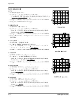
1. PD
1) TPL6-OSC & OSC mode
2) - Connect the probe of oscilloscope to TPL-OSC.
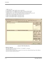
- Press the UP/DOWN button or the number buttons so that the A is
2.0µs ± 0.2µs (when NTSC)
.
3) Using the UPDATE button, store the adjusted value in the EEPROM.
* Using OSC or CSHD, adjust the trigger.
2. BRIGHTNESS
1) TPL2-VG & RGB-AMP mode
2) - Connect the probe of oscilloscope to TPL2-VG.
- Press the UP/DOWN button or the number buttons so that the B
level (between blacks) is 3.5 ± 0.1Vp-p.
3) Using the UPDATE button, store the adjusted value in the EEPROM.
* Using FRP(or use No. 2 - 7 alignment wave form in common), adjust
the trigger.
3. CONTRAST
1) TPL2-VG & CONTRAST mode
2) - Connect probe of oscilloscope to TPL2-VG.
- Press the UP/DOWN button or the number buttons so that the C
level (between black and white) is 3.0 ± 0.1Vp-p.
3) Using the UPDATE button, store the adjusted value in the EEPROM.
4. R-BRIGHT
1) TP3-VR & R-BRT mode (Bright wave form)
2) - Connect the probe of oscilloscope to TP3-VR.
- Press the UP/DOWN button or the number buttons so that the B
level (between pedestals) is 3.5 ± 0.1Vp-p.
3) Using the UPDATE button, store the adjusted value in the EEPROM.
5. R-CONTRAST
1) TPL3-VR & R-CONT mode (Contrast wave form)
2) - Connect the probe of oscilloscope to TPL3-VR.
- Press the UP/DOWN button or the number buttons so that the C
level is 3.0 ± 0.1Vp-p.
3) Using the UPDATE button, store the adjusted value in the EEPROM.
6. B-BRIGHT
1) TPL1-VB & B-BRT mode (Bright wave form)
2) - Connect the probe of oscilloscope to TPL1-VB.
- Press the UP/DOWN button or the number buttons so that the B
level is 3.5 ± 0.1Vp-p.
3) Using the UPDATE button, store the adjusted value in the EEPROM.
PD wave form
BRIGHT wave form
CONTRAST wave form
Summary of Contents for SDC-80
Page 9: ...Samsung Electronics 2 2 Specifications MEMO MEMO ...
Page 21: ...Samsung Electronics 5 6 Adjustment MEMO MEMO ...
Page 34: ...Samsung Electronics 7 12 PCB Diagrams MEMO MEMO ...
Page 35: ...Samsung Electronics 8 1 8 Wiring Diagram ...
Page 36: ...Samsung Electronics 8 2 Wiring Diagram MEMO MEMO ...
Page 38: ...Samsung Electronics 9 2 Schematic Diagrams 9 2 9 1 Process Block Rev 02 03 Rev 02 Rev 03 ...
Page 39: ...Samsung Electronics 9 3 Schematic Diagrams 9 2 Drive Block Rev 02 03 ...
Page 40: ...Samsung Electronics 9 4 Schematic Diagrams 9 3 Mevory Block Rev 02 ...
Page 41: ...Samsung Electronics 9 5 Schematic Diagrams 9 4 Memory Block Rev 03 ...
Page 42: ...Samsung Electronics 9 6 Schematic Diagrams 9 5 LCD Block Rev 02 03 ...
Page 43: ...Samsung Electronics 9 7 Schematic Diagrams 9 6 Back Light Block Rev 02 03 ...
Page 44: ...Samsung Electronics 9 8 Schematic Diagrams 9 7 DC Block Rev 02 03 ...
Page 45: ...Samsung Electronics 9 9 Schematic Diagrams 9 8 Charge Block Rev 02 03 ...
Page 46: ...Samsung Electronics 9 10 Schematic Diagrams 9 9 Function Block Rev 02 03 ...
Page 47: ...Samsung Electronics 9 11 Schematic Diagrams 9 10 Jack Block Rev 02 03 ...


