background image

Troubleshooting

Samsung Electronics

6-13

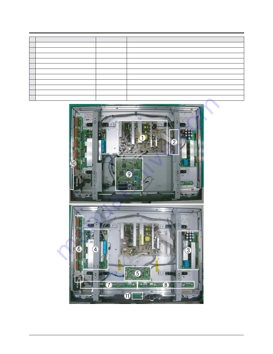
6-3 Troubleshooting Procedures by ASS'Y

No

Assy

Description

Major Symptoms

1 ASSY PCB P-SMPS

Main SMPS

No power, Blank screen, the Relay repeats On and Off.

2 ASSY PCB P-SMPS

DC-DC SMPS

Blank screen, the Relay repeats On and Off.

3 ASSY PDP MODULE P-X MAIN BOARD

X Main Board

Blank screen

4 ASSY PDP MODULE P-X MAIN BOARD

Y Main Board

Blank screen

5 ASSY PDP MODULE P-LOGIC MAIN

Logic Board

Blank screen, Screen noise

6 ASSY PDP MODULE P-Y MAIN SCAN BUFFER

Y Scan Board

Row Bar screen is blank

7 ASSY PDP MODULE P-ADDRESS E BUFFER

Address E Buffer Board Corresponding Buffer Board block screen is blank.

8 ASSY PDP MODULE P-ADDRESS F BUFFER

Address F Buffer Board Corresponding Buffer Board block screen is blank.

9 ASSY PCB MISC-MAIN

Main Board

No Power, Abnormal screen for each input source, PIP screen trouble, Sound trouble

10 ASSY BOARD P-FUNCTION

Function Key Board

The side function key does not work properly

11 ASSY BOARD P-POWER&IR

Power Button Board

The remote control does not work properly, the LED does not work properly.

Summary of Contents for PS42C6HX/XEC

Page 1: ...onvenience Quality RF HDMI 2 Scart PC Analog Component Video S Video Slim line design Energy Saving VHUYLFH Pdqxdo PS 42C6H SGS0WHOHYLVLRQ Fkdvvlv G 7D SbHxurshb75KG bDxgl Prgho SV75F9K 2 HF Refer to...

Page 2: ...tic law Samsung Electronics Co Ltd May 2005 Printed in Korea AA82 04680A Area Web Site North America service samsungportal com Latin America latin samsungportal com CIS cis samsungportal com Europe eu...

Page 3: ...ow to Access Service Mode 3 2 3 3 Factory Data 3 3 3 4 Service Adjustment 3 8 3 5 Software Upgrade 3 11 3 6 Replacements Calibration 3 12 Chapter 4 Exploded View Part List 4 1 PS42C6HX XEC 4 1 Chapter...

Page 4: ...ration Instruction Installation 11 1 Product Features and Functions 11 1 11 2 Installation Notes and Precautions 11 4 Chapter 12 Disassembly Reassembly 12 1 Overhaul Disassembly Reassembly 12 1 Chapte...

Page 5: ...nt Adjustment 3 1 Service Instruction Before Performing After Sales Services 1 Check if the measurement and test equipment is working properly 2 Secure sufficient work space for disassembling the prod...

Page 6: ...nel Key Select an item Volume Key Adjust the value up or down MENU Key Save the changes to the EEPROM and return to the higher level mode Using the Numeric 0 9 keys you can select a channel Using the...

Page 7: ...TTX Level L1 5 PS Test MIN LED OnTime 10 LED OffTime 0 Debug Smart Ch Table SUWON iDTV Country UK ACR OFF 3 White Balance Adjustment White Balance Range 0 255 Sub Bright 128 R off set 128 G off set 12...

Page 8: ...7CH 7BH 80H 9DH ADC Calibration RF AV COMP PC HDMI TCD3 Contrast 84H 78H 78H 78H TCD3 Brightness 23H 20H 20H 20H TCD3 CR 80H 80H 80H 80H TCD3 CB 80H 80H 80H 80H TCD3 Delay 00H 00H 00H 00H Analog Y Of...

Page 9: ...CHM Gain2 45H ColorGain TY 00H ColorGain TC 00H ColorGain TM 00H Color Gain 80H Input RGB Gain 80H Input RGB Offset 00H 6 STV8257 STA323W Sound IC Correct Register Ch1 Volume 55H Ch2 Volume 55H AGC Ga...

Page 10: ...L L 66H NTSC 3 58 96H NTSC 4 43 CCH AV PAL A9H AV SECAM 66H AV NT3 58 98H AV NT4 43 CCH AV PAL60 77H 8 Adjust V Mute Time 10 Melody Volume 9 Ana_Dimm_Max FEH TTX Contrast 50 TTX Brightness 50 TTX Colo...

Page 11: ...Min Sec 10 W B MOVIE RF AV COMP PC HDMI WB Movie OFF OFF OFF OFF Color Mode Movie Movie Movie Movie Color Tone Warm2 Warm2 Warm2 Warm2 W1 R Gain 130 129 130 134 W1 B Gain 117 118 119 120 W1 R Offset...

Page 12: ...ting Mode PAL Video MODE 2 3 Pattern Pattern 24 Chess Pattern 4 Use Equipment K 7256 or Equipment of equality level 5 Work order 1 Enter by Factory Mode select 1 CALIBRATION 2 Select AV CALIBRATION ag...

Page 13: ...MI DVI 1280 720 60Hz Test Pattern MSPG 945 Series Pattern 16 Color temperature 1500K 500 6 20 MPCD Color coordinate H L 270 280 2 L L 270 280 3 2 1 Ft 0 05 Ft SAMSUNG WHITE BALANCE Adjustment PATTERN...

Page 14: ...color control confirm the data c Adjust the low light Refer to table 1 2 in adjustment position by mode Adjust sub Brightness to set the Y value Adjust red offset x and blue offset y to the color coor...

Page 15: ...are Upgrade 3 5 1 How to Update Flash ROM 1 Installthe Flash Downloader Connect Set Service Jack and Jig Cable to execute Program Update 2 Flash Downloader program update Before Turning on the set Cli...

Page 16: ...43A Vs Va voltage check and adjust ASSY PCB P SMPS DC DC BN96 01856A Output voltage check and adjust ASSY PDP P LOGIC BOARD BN96 04177A Not adjustment ASSY PDP P X MAIN BOARD BN96 03350A ASSY PDP P Y...

Page 17: ...el voltages must be adjusted after changing SMPS PCB or PDP module Value Board Adjustment Vs 200 SMPS MAIN Va 65 Vset 195 SMPS DC DC Ve 120 Vscan 190 SMPS DC DC Voltage Label SMPS MAIN 2 A point of ad...

Page 18: ...Adjustment 3 14 Samsung Electronics 3 A point of adjusting SMPS DC DC Use base chassis of PDP panel as GND point Test Point Vset Middle Vscan Right Ve Test Point Vscan Vset Adjustment Point VE Adjustm...

Page 19: ...insulated transformers the product can only be repaired safely when the chassis is connected to the earth end of the AC power source To make sure the AC power cord is properly connected follow the ins...

Page 20: ...placed with another irregular one the safety or protective features will be lost even if the new one has a higher voltage or more watts Critical safety parts should be bracketed with Use only regular...

Page 21: ...stance between the blade of the AC plug and that of the conductive material should be more than 1 7 Any B interlock should not be damaged If the metal heat sink is not properly installed no connection...

Page 22: ...s for soldering purposes 6 Use only anti static solder removal devices Most solder removal devices do not support an anti static feature A solder removal device without an anti static feature can stor...

Page 23: ...sitioning the product Also check the antenna cable or the external connectors if they are fully unplugged Damage to the cord may cause fire or electric shock 6 Keep the antenna far away from any high...

Page 24: ...1 6 Samsung Electronics MEMO...

Page 25: ...N BOARD BN96 03550A 42HD PL42AX005A V5 1 NTSC PAL 1024 768 LJ92 01345A ASSY PDP MODULE P Y MAIN BOARD BN96 03351A 42HD PL42AX005A V5 1 NTSC PAL 1024 768 LJ92 01346A ASSY PDP MODULE P Y MAIN SCAN BUFFE...

Page 26: ...CN5007 Y B D Pin No Signal 1 Vs 2 Vs 3 RTN 4 RTN 5 Vset 6 RTN 7 Vscan 8 RTN 9 Vg 10 D5 3V CN4 DC DC SMPS CN4001 X B D Pin No Signal 1 D5 3V 2 Vg 3 RTN 4 RTN 5 Ve 6 RTN 7 RTN 8 Vs 9 Vs CN6 DC DC SMPS C...

Page 27: ...2 2 Connect Cables Use SMPS 12P LVDS 31P POWER 10P Code BN39 00632B BN39 00667D BN39 00675A Photo Use POWER 12P GROUND WIRE Code BN39 00676A BN39 00164A Photo The code number of cable Lead connector c...

Page 28: ...8 4 Samsung Electronics MEMO...

Page 29: ...TSC PAL and SECAM a HDTV sync separator motion adaptive de interlacing engine and the video format conversion engine supporting multi window display in many different output modes STV8257DSX IC503 Dig...

Page 30: ...oltage EU AC 220 240V 50Hz CIS AC 100 240V 50 60Hz Colour System PAL SECAM NT3 58 NT4 43 Sound System BG DK I L Number of Pixels 1024 H X 768 V ANTENNA input VHF UHF 75 unbalanced VIDEO input SCART1 S...

Page 31: ...ace Picture Enhancement FBE Still picture Noise reduction Comb Filter 3D comb filter PIP Large Panorama Wide Sound System Stereo Output 10W 10W Speaker built in Feature Component Interface 480i 480p 5...

Page 32: ...72 809 37 861 N N 75 000 37 500 N N 800 X 600 56 250 35 156 N P N P 60 317 37 879 P P 70 000 43 75 N P N P 72 188 48 077 P P 75 000 46 875 P P 848 x 480 60 000 31 020 P P 74 769 37 684 P N 1024 X 768...

Page 33: ...59 2 Kg Picture Brightness 1 100 Cd m2 1 300 Cd m2 Contrast Ratio 5000 1 10 000 1 Image Enhacer FBE DNIe L Audio Equalizer O O Auto Volume O O Surround Sound SRS TruSurround SRS TruSurround Speaker Ou...

Page 34: ...ty Card Registration Card Safety Guide Manual BN68 00514C AA68 03575A AA68 03242E Ferrite Core for Power Cord BN63 01798A Accessories that can be purchased additionally Audio Cables BN39 00149A Electr...

Page 35: ...3D digital comb video decoder that supports NTSC PAL and SECAM a HDTV sync separator motion adaptive de interlacing engine and the video format conversion engine supporting multi window display in man...

Page 36: ...rd Pin No Signal 1 6 5V 2 RTN 3 12V 4 RTN 5 18Vamp 6 18Vamp 7 RTN_amp 8 RTN_amp 9 Vt 10 RTN CN2013 Logic B d CN902 Main Board Pin No Signal Pin No Signal Pin No Signal 1 GND 12 TXOUT2 23 TXOUT0B 2 GND...

Page 37: ...Board CN001 Power Button Pin No Signal 1 GND 2 LED 3 ST5V 4 GND 5 KEY_INPUT2 6 7 8 IR_7414 CN501 Main Board Speaker Out Pin No Signal 1 SPK_R 2 SPK_R 3 SPK_L 4 SPK_L CN741 Main Board CN1 Function Boar...

Page 38: ...Description RM1 Remote Control Sensor SW1 Power Button OP1 The Illumination sensor that senses the quantity of light It senses the illumination and automatically adjusts the screen brightness accordin...

Page 39: ...6 RTN 7 12V 8 PS_ON 9 RTN 10 STBY 11 FAN_ON 12 FAN_D CN803 Main SMPS CN101 Main Board Pin No Signal 1 6 5V 2 RTN 3 12V 4 RTN 5 18Vamp 6 18Vamp 7 RTN_amp 8 RTN_amp 9 Vt 10 RTN CN810 Main SMPS CN2013 L...

Page 40: ...5 3V 2 Vg 3 RTN 4 RTN 5 RTN 6 RTN 7 RTN 8 Va 9 Va 10 N C 11 Vs 12 Vs CN2 DC DC SMPS CN5007 Y SMPS Pin No Signal 1 5 3V 2 Vg 3 RTN 4 Vscan 5 RTN 6 Vset 7 RTN 8 RTN 9 Vs 10 Vs CN4 DC DC SMPS CN4001 X S...

Page 41: ...Y PDP MODULE P X MAIN BOARD X Drive Board ASSY PDP MODULE P Y MAIN BOARD Y Drive Board ASSY PDP MODULE P Y MAIN SCAN BUFFER Y Buffer Board ASSY PDP MODULE P ADDRESS E BUFFER Address Buffer Board ASSY...

Page 42: ...9 8 Samsung Electronics MEMO...

Page 43: ...user receives HD rated broadcasts The digital distributed TV Ready Technique can render HD sources as HD rated However you need to install a set top box for this purpose The digital TV alone cannot r...

Page 44: ...console through a wide TV by selecting the aspect ratio to normal 4 3 or wide 21 9 the left and right or top and bottom of the picture will not be displayed This symptom appears in other manufacturer...

Page 45: ...g is a television broadcasting signal digitized and transmitted according to the United States terrestrial digital broadcast standard or ATSC Mono A type of audio interface that transmits the audio si...

Page 46: ...smatch on the TV Progressive Scan Progressive scan displays the entire frame in a single sweep so as to provide clearer and sharper visual quality DVD Digital Versatile Disc DVD is a large capacity st...

Page 47: ...ree primary colors of light R G and B the number of possible colors for a pixel is 256 x 256 x 256 16 777 216 or 16 7 million colors If 12 bits are used for a pixel the gradation is 212 or 4096 for a...

Page 48: ...of the signal broadcast from a broadcast station is smaller than that of possible color coordinates Moreover a TV provides a smaller color coordinate area than that of the signal from the broadcastin...

Page 49: ...a disconnected cable connection or a connection is too loose Check to see if the cables are connected according to the connection diagram 2 Check the power input to the Main Board 3 Check the voltage...

Page 50: ...e cables are improperly connected or the Main Board or SMPS is out of order In this case check the following Check the internal cable connection status inside the unit Check the fuses of each part Che...

Page 51: ...d and CN of the Y Main Board a spark may be generated by the electric charge of the high capacity capacitor Therefore wait some time after separating the power cord from the unit Does the symptom cont...

Page 52: ...eparating and connecting the cables such as CN809 of the Main SMPS CN1 CN2 CN3 CN4 and CN5 of the DC DC SMPS CN of the X Main Board and CN of the Y Main Board a spark may be generated by the electric...

Page 53: ...in Board is out of order Speaker defect When setting the volume to 0 Nonsense Troubleshooting Procedures Is the cable connection between the Main Board and the speaker properly connected Is the output...

Page 54: ...cklist Check the antenna connection settings Antenna 1 Normal Cable DTV Antenna 2 Only for DTV Check the tuner output signal CVBS Check the power input of the Main board Troubleshooting Procedures Che...

Page 55: ...eck the U101 D108 PFC Normal Abnormal Check the U201 Q203 Q204 Power ON VA Multi Check the U501 Abnormal Abnormal Check the U601 Normal VS Normal Abnormal Check the Q401 Q402 Check the Other board Ima...

Page 56: ...age not open or short is no screen Y MAIN X MAIN Logic Main Sustain Open Some horizontal lines don t exist on screen Scan Buffer FPC of X Y Sustain Short Some horizontal lines appear to be linked on s...

Page 57: ...the FUSE Check the input voltage YES NO YES NO Y MAIN Check several points FUSE FET DIODE Y MAIN Normal State Replace the Board Replace the Board OK OPEN SHORT OK F5001 for VDD F5002 for Vs F5004 for...

Page 58: ...oard Replace the Board OK OPEN SHORT OK F5001 for VDD F5002 for Vs F5004 for VCC F5005 for OUT_L Q5009 Q5021 X MAIN Check several points FUSE FET X MAIN Normal State Replace the Board Replace the Boar...

Page 59: ...ffer recheck the status Done Defect is from Y buffer Replace the Panel There a defect on FPC OK NG Sustain Short some horizontal lines appear to be linked on Video Y FPC Sustain Short Discharging in u...

Page 60: ...internal mode screen is normal Reload the data onto the MICOM and recheck it Check if there is an open or short circuit on the Buffer Board and the Logic Main address data output section Check the FF...

Page 61: ...screen Screen noise 6 ASSY PDP MODULE P Y MAIN SCAN BUFFER Y Scan Board Row Bar screen is blank 7 ASSY PDP MODULE P ADDRESS E BUFFER Address E Buffer Board Corresponding Buffer Board block screen is...

Page 62: ...6 14 Samsung Electronics MEMO...

Page 63: ...ference 3V3 Voltage for Logic Control Vcc Voltage for FETdriver Va Voltage for address pulse Vs Voltage for sustain pulse Vsc Voltage for scan pulse Ve Voltage for X ramp pulse Vset Voltage for Y ramp...

Page 64: ...5 18Vamp 6 18Vamp 7 RTN_amp 8 RTN_amp 9 Vt 10 RTN CN810 Main SMPS CN2013 Logic Board Pin No Signal 1 STBY 2 VS_ON 3 N C 4 PS_ON 5 RTN 6 5 3V 7 RTN 8 RTN 9 5 3V 10 5 3V CN2 DC DC SMPS CN5007 Y B D Pin...

Page 65: ...r P o i d u A 7 5 2 8 V T S s m 0 2 1 c n y S p i L p m A P H 0 5 0 7 A D T F I S B M 6 1 R D D D 8 3 2 3 6 2 D 4 K r e n u T F R o i d u A W S 2 5 0 4 C H r e n u T A N A F R t u o o d i u A e c i v...

Page 66: ...Block Diagram 7 4 Samsung Electronics 7 2 3 Module Driver Board Block Diagram 1 Y Main Board 2 X Main Board...

Page 67: ...nnector 10 Pin Power 31 Pin LVDS SPS NIRB ASIC 816P DDR DRIVE RESET FA DDR MA DDR MB R G B 24bit CLK 1 2 BLK POC STB CSE CE1 CE2 R G B 24bit CLK 1 2 BLK POC STB CSE CE1 CE2 DATA 32bit ADDR 12bit DQS C...

Page 68: ...7 6 Samsung Electronics MEMO...

Page 69: ...OUTPUTS Va Vg vs 3 4V turn off sequence Vca Vcs Keep Display ON w o display flicker while 3cycle full dip condition Standby step turn off for processor reset 1 When connecting the AC power cord Stand...

Page 70: ...eak loading at 90V AC The power supply shall automatically recover from AC power loss Note that nominal voltages for test purposes are considered to be with 1 0V of nominal STD_5V Vpr2 3 3V is a SELV...

Page 71: ...r supply The power supply shall either shutdown and latch off for shorting is removed the P S shall recover The power supply shall be capable of withstanding a continuous short circuit to the output w...

Page 72: ...M Initial image option PIN Initial image select F W or BLACK Jumper Yes or Full White Jumper No Black Micom Loading 5Pin Connector or Uart Connector The connector to load the Micom drive program The p...

Page 73: ...y displayed Therefore you have to conduct a short test for each part If the Vref voltage Voltage Divider Voltage is lower than 1 25V check the resistance of the resistance output part and check if the...

Page 74: ...That is the pixel whose wall charge has been formed by the Address Discharge forms a Sustain Discharge vis the following Sustain pulse 2 Sustain Discharge A Sustain Discharge is a Self Sustaining Dis...

Page 75: ...function of each board Y Pole Terminal 6 Block X Pole Terminal 2 Block Power B d Logic B d Logic E Buffer Logic F Buffer Sustain Pulse Energy Recovery Rising Ramp Pulse Falling Ramp Pulse Vscan Pulse...

Page 76: ...PC output electrodes sequentially one line at a time At this time Vscan is called the Scan Bias Voltage A Vscan voltage of approximately 175 Volt Vsc_1 is supplied to the electrode lines For the other...

Page 77: ...ce 0 2 When no signal is output to the gate GND FET changes to an open circuit i e an insulator of resistance High Voltage Switching of the FET Operation 1 When no signal is applied to G1 FET1 is open...

Page 78: ...Circuit Description 13 10 Samsung Electronics 1 Vs 2 Vs 3 DGND 4 DGND 5 Ve 6 DGND 7 DGND 8 Vcc CN4003 Signal 140mm 280mm 8 1 CN4004 Power CN4002 CN4001 Drive Board Connector Layout 1 X Main Board...

Page 79: ...11 CN5506 Panel CN5505 Panel CN5504 Panel CN5503 Panel CN5502 Panel CN5501 Panel CN5010 Panel 280mm CN5013 signal 1 9 CN5011 CN5509 CN5010 190mm CN5012 CN5508 CN5507 CN5004 9 Vs 8 Vs 7 GND 6 GND 5 Vse...

Page 80: ...120usec 70usec Vsc_h Variable register Falling ramp Variable register Rising ramp Variable register Vset Vs Vsc_l Vsc_h Ve Va 195V 200V 190V 70V 120V 65V Adjust the drive waveform so that the main res...

Page 81: ...Circuit Description Samsung Electronics 13 13 X OUT Check that the output of X Out of the X board follows the waveform of Attachment 2 when the power is supplied...

Page 82: ...Circuit Description 13 14 Samsung Electronics Attachment 1 Y Output Waveform Rising Ramp Falling Ramp Rising Ramp Falling Ramp...

Page 83: ...Circuit Description Samsung Electronics 13 15 Scan_l Even_Scan Y Sustain...

Page 84: ...Circuit Description 13 16 Samsung Electronics Attachment 2 X Output Waveform X Sustain...

Page 85: ...4A ASSY PDP MODULE P 42HD W1 1024 768 compl 1 S A T0074 BN59 00539A REMOCON AUDI TM87B SAMSUNG 54Key 31mArms 1 S A T0079 BN94 01364A ASSY PCB MISC MAIN PS 42C6H EU D74A BN41 1 S A T0159 BN96 01856A AS...

Page 86: ...Samsung Electronics 5 2 MEMO...

Page 87: ...not to damage the cables Take care not to cause a flaw in the Glass Filter in the front Assemble the boards in the reverse order of the disassembly The plasma must be layed down on a flat padded surf...

Page 88: ...nput 4 40 L6 NI PLT C3601 Remove Bracket Terminal 12 1 4 Separation of ASSY PCB MISC MAIN Part Name Description Description Photo Main Board Detach all connectors from the Main Board Remove 4 screws P...
Page 89: ...scription Description Photo FILTER EMI AC LINe Detach connector from Main SMPS Remove 2 screws PH WWP M3 L8 NI PLT Remove a screw BH S M4 L10 ZPC BLK Remove FILTER EMI AC LINE 12 1 8 Separation of ASS...

Page 90: ...P POWER IR Part Name Description Description Photo Power IR Board Remove 2 screw BH S M4 L8 ZPC BLK Remove the Power IR Board 12 1 9 Separation of ASSY SPEAKER P Part Name Description Description Pho...

Page 91: ...ctors from the Assy SMPS DC DC Board Remove 4 screws PH WWP M3 L8 NI PLT Remove the SMPS DC DC Board Wear gloves when handling the power board as there may be some remaining electrical charge in the c...

Page 92: ...ULE P X MAIN BOARD Part Name Description Description Photo Flat Cable Detach all Connectors from the X Main Board To separate the Flat Cable of the X Board press the upper and the lower sides of the c...

Page 93: ...ARD Part Name Description Description Photo Flat Cable Detach the 6 scan board connectors from the panel by pulling the holder from both the top and bottom ends Y Scan Remove 2 screws PH WWP M3 L8 NI...

Page 94: ...ASSY PDP MODULE P ADDRESS BUFFER BOARD Part Name Description Description Photo Still Bar Remove 3 screws PH WWP M3 L8 NI PLT Remove the still bar Buffer Detach the all connectors from the buffer boar...

Page 95: ...TAND 42C7 HGI T2 0 1 S N A M0145 BN96 02784B ASSY BOARD P FUNCTION CADILLAC SJ06 01 0 1 S A M0150 BN96 04343A ASSY BRACKET P FILTER BOTTOM 42C7 AL 1 S N A T0003 BN96 03762P ASSY COVER P FRONT 42C6H HQ...

Page 96: ...V 6 1 F n 0 0 1 3 5 1 C V 6 1 F u 0 0 1 2 5 1 C 1 0 1 D V 6 1 F u 0 0 1 7 4 1 C R104 100Kohm V 5 2 F n 0 0 1 1 3 1 C 3 1 1 D B 4 1 1 C V 0 5 F n 0 0 1 T 5 1 0 L 2 1 0 2 B C A 1 0 1 D B T J 1 2 1 2 3...

Page 97: ...C S 1 K L C S 6 1 D D V 1 S S V 7 8 T U O X 9 N I X 37 P3 5 PWM5 2 P3 6 PWM6 2 38 NC 39 4 2 0 A D S 1 T A D S 40 P1 4 VSYNC O P1 5 HSYNC O 41 P1 6 CLAMP O 42 43 1 T N I 1 0 P 3 0 3 6 2 P 7 2 P 1 3 2...

Page 98: ...6 1 C S K 1 0 3 Q 6 2 3 R m h o K 0 1 6 0 0 1 U 1 0ohm R396 1 H T G 0 3 C 3 S D C 9 4 3 D 8 5 3 P T 9 7 3 P T 1 m h o 5 7 1 5 3 R W 0 1 1 m h o 0 0 1 6 0 4 R 1 m h o K 8 1 2 4 3 R H T G 0 3 C 3 S D C...

Page 99: ...3 4 4 P T 1 2 3 4 D 1 1 3 4 D 1 2 3 2 3 4 P T 1 1 4 4 D 1 2 3 W 0 1 1 2 2 0 1 U 1 m h o K 7 4 1 5 4 R 0 2 4 D 0 3 4 R m h o K 0 1 m h o 0 1 4 6 4 R 6 6 4 R m h o 0 1 1 6 4 R m h o 0 1 m h o 6 5 8 3 4...

Page 100: ...S V N G I S C C V 6 3 B 2 C C V 4 C N 5 B 2 D N G 6 7 A 2 D N G A 2 C C V 8 A 2 T U O 9 A D N G 9 2 A D D V 3 B 2 T U O 0 3 I D S I K C R L 1 3 2 3 I K C I V D N G 3 3 4 3 D D V 5 3 1 2 G I F N O C T...

Page 101: ...F 195 VDDR 196 MA11 197 MA10 198 MA9 199 MA8 5 8 1 8 2 D M 6 8 1 9 2 D M 7 8 1 0 3 D M 8 8 1 1 3 D M 9 8 1 0 K L C M 9 1 1 G _ Y 0 9 1 O K L C M 1 9 1 C D D V 8 7 1 5 2 D M 9 7 1 6 2 D M 8 1 4 C D A _...

Page 102: ...0 0 1 V 6 1 7 3 6 R m h o 0 0 4 6 R m h o 0 F n 1 5 2 6 C V 0 5 3 3 6 R m h o 0 F u 0 1 9 5 6 C D V 3 3 B V 6 1 3 2 6 C F n 0 0 1 F E R X F E R X F E R X F E R X F E R X R628 1 10W 100ohm 100ohm 1 10W...

Page 103: ...3 1 8 R m h o 0 9 0 8 L V 6 1 F u 0 0 1 4 3 8 C m h o 0 2 0 8 R L L P _ V 2 1 A V 5 2 1 3 8 C F n 0 0 1 2 N I 3 W S D N G 4 B F 5 P M O C 6 7 N E 8 S S 1 D N G M 4 0 8 C I N D 3 8 5 1 P M 1 S B 4 1 8...

Page 104: ...Q D D V 9 5 3 3 Q D D V 4 Q D D V 1 4 9 4 5 Q D D V 6 Q D D V 5 5 7 Q D D V 5 7 1 8 8 Q D D V 4 4 1 S S V 4 1 1 C _ N 2 C _ N 1 2 0 3 3 C _ N 4 C _ N 7 5 5 C _ N 9 6 6 C _ N 0 7 7 C _ N 3 7 _ S A R 9...

Page 105: ...F E R X F E R X F p 5 1 V 0 5 5 6 7 8 9 1 D N G M 2 D N G M 4 2 5 2 6 2 7 2 8 2 9 2 3 0 3 1 3 4 4 1 5 1 6 1 7 1 8 1 9 1 2 0 2 1 2 2 2 3 2 1 0 1 1 1 2 1 3 1 1 0 9 N C 1 2 3 V 3 3 1 0 9 T F A 2 4 0 1 E...

Page 106: ...W 0 1 1 3 E O 0 1 1 1 B 4 A 4 2 1 3 1 4 E O C C V 4 1 A 1 2 B 1 3 1 3 0 0 1 C I X M 5 2 1 3 T S F 1 E O 1 4 0 0 1 D B 1 A B 2 C C V _ V 5 B 1 F E R X 50V C1303 33pF 4 2 S S 3 0 0 1 D 1 F u 0 0 1 1 2 0...

Page 107: ...ee the on screen menu of your TV s features 3 Press to decrease or increase the volume In the on screen menu use the buttons as you use the and buttons on the remote control 4 C P Press to change chan...

Page 108: ...e optional HDMI DVI adapter the DVI analog audio inputs on your TV allow you to receive left and right audio from your DVI device Not compatible with PC When connecting this product via HDMI or DVI to...

Page 109: ...ote control TV DVD STB CABLE VCR 18 Available source selection 19 Previous channel 20 Automatic Power off 21 Selects the PC mode directly 22 VCR DVD Function Rewind Stop Play Pause Fast Forward 23 Nex...

Page 110: ...ed on plaster or wood 4 The package contents and parts supplied for the wall mount are subject to change without prior notice 11 2 2 Mounting Kits Wall Mount Bracket Plastic Hanger 4 EA SCREW 4 EA ASS...

Page 111: ...fingers while installing and adjusting the angle 4 Please tightly secure the wall mount bracket to the wall to avoid injury from a falling SET 3 Tighten the screws of the plastic hanger shown in pict...

Page 112: ...fety pins underneath the PDP If the safety pins are not removed the angle cannot be adjusted Any attempt to do so may cause damage to the PDP 2 Hold onto the bottom of the PDP and pull forward fully a...

Page 113: ...onvenience Quality RF HDMI 2 Scart PC Analog Component Video S Video Slim line design Energy Saving VHUYLFH Pdqxdo PS 42C6H SGS0WHOHYLVLRQ Fkdvvlv G 7D SbHxurshb75KG bDxgl Prgho SV75F9K 2 HF Refer to...

Page 114: ...tic law Samsung Electronics Co Ltd May 2005 Printed in Korea AA82 04680A Area Web Site North America service samsungportal com Latin America latin samsungportal com CIS cis samsungportal com Europe eu...

Page 115: ...ow to Access Service Mode 3 2 3 3 Factory Data 3 3 3 4 Service Adjustment 3 8 3 5 Software Upgrade 3 11 3 6 Replacements Calibration 3 12 Chapter 4 Exploded View Part List 4 1 PS42C6HX XEC 4 1 Chapter...

Page 116: ...Chapter 9 PCB Diagram 9 1 Main Board 9 1 9 2 Power IR Board 9 4 9 3 Function Board 9 4 9 4 Main SMPS Board 9 5 9 5 DC DC SMPS Board 9 6 9 6 PDP Module 9 7 Chapter 10 Schematic Diagram 10 1 Analog 10 1...

Reviews: