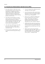
1-3 Precautions for Electrostatically Sensitive Devices (ESDs)
1. Some semiconductor (“solid state”) devices
are easily damaged by static electricity. Such
components are called Electrostatically
Sensitive Devices (ESDs); examples include
integrated circuits and some field-effect
transistors. The following techniques will
reduce the occurrence of component damage
caused by static electricity.
2. Immediately before handling any semicon
ductor components or assemblies, drain the
electrostatic charge from your body by
touching a known earth ground. Alternatively,
wear a discharging wrist-strap device. (Be
sure to remove it prior to applying power—
this is an electric shock precaution.)
3. After removing an ESD-equipped assembly,
place it on a conductive surface such as
aluminum foil to prevent accumulation of
electrostatic charge.
4. Do not use freon-propelled chemicals. These
can generate electrical charges that damage
ESDs.
5. Use only a grounded-tip soldering iron when
soldering or unsoldering ESDs.
6. Use only an anti-static solder removal device.
Many solder removal devices are not rated as
“anti-static”; these can accumulate sufficient
electrical charge to damage ESDs.
7. Do not remove a replacement ESD from its
protective package until you are ready to
install it. Most replacement ESDs are
packaged with leads that are electrically
shorted together by conductive foam,
aluminum foil or other conductive materials.
8. Immediately before removing the protective
material from the leads of a replacement ESD,
touch the protective material to the chassis or
circuit assembly into which the device will be
installed.
9. Minimize body motions when handling
unpackaged replacement ESDs. Motions such
as brushing clothes together, or lifting a foot
from a carpeted floor can generate enough
static electricity to damage an ESD.
Precautions
1-4
Samsung Electronics
Summary of Contents for PCL545RX/XAA
Page 2: ...ELECTRONICS Samsung Electronics Co Ltd AUG 2001 Printed in Korea AA68 ...
Page 11: ...Reference Information Samsung Electronics 2 5 2 3 MICOM IIC BUS LINE UP ...
Page 12: ...Reference Information 2 6 Samsung Electronics MENO ...
Page 14: ...Specifications 3 2 Samsung Electronics MENO ...
Page 38: ...Alignment and Adjustments 4 24 Samsung Electronics ...
Page 39: ...Alignment and Adjustments Samsung Electronics 4 25 ...
Page 40: ...Alignment and Adjustments 4 26 Samsung Electronics ...
Page 41: ...Alignment and Adjustments Samsung Electronics 4 27 1 4 8 2 Perfect Focus Factory Mode ...
Page 42: ...Alignment and Adjustments 4 28 Samsung Electronics 2 3 4 ...
Page 58: ...Alignment and Adjustments 4 44 Samsung Electronics MENO ...
Page 62: ...MEMO 5 4 Samsung Electronics ...
Page 67: ...Exploded View Part List Samsung Electronics 6 5 6 5 HCL47WX XAA HCL4715WX XAA ...
Page 69: ...Exploded View Part List Samsung Electronics 6 7 6 7 HCL552WX XAA HCL5515WX XAA ...
Page 71: ...Exploded View Part List Samsung Electronics 6 9 6 9 HCL652WX XAA HCL6515WX XAA ...
Page 162: ...7 90 Samsung Electronics MEMO ...
Page 163: ...Samsung Electronics Block Diagrams 8 1 8 Block Diagram 8 1 Main Signal Progressive ...
Page 164: ...Block Diagrams 8 2 Samsung Electronics 8 2 Video Signal ...
Page 165: ...Samsung Electronics Block Diagrams 8 3 8 3 Sound Signal ...
Page 170: ...8 8 Video S W Signal Change Block Diagrams 8 8 Samsung Electronics ...
Page 177: ...10 Schematic Diagrams Samsung Electronics Schematic Diagrams 10 1 10 1 MAIN 1 ...
Page 178: ...Schematic Diagrams 10 2 Samsung Electronics 10 2 MAIN 2 ...
Page 179: ...Samsung Electronics Schematic Diagrams 10 3 10 3 MAIN 3 TP02 TP01 TP01 TP02 ...
Page 180: ...Schematic Diagrams 10 4 Samsung Electronics 10 4 MAIN 4 ...
Page 181: ...Samsung Electronics Schematic Diagrams 10 5 10 5 MICOM TP04 TP03 TP03 TP04 ...
Page 182: ...Schematic Diagrams 10 6 Samsung Electronics 10 6 POWER ...
Page 183: ...Samsung Electronics Schematic Diagrams 10 7 10 7 SOUND ...
Page 184: ...Schematic Diagrams 10 8 Samsung Electronics 10 8 CRT ...
Page 185: ...Samsung Electronics Schematic Diagrams 10 9 10 9 3D COMB ...
Page 188: ...Schematic Diagrams 10 12 10 11 SUB 2 TP14 TP13 TP13 TP14 ...
Page 190: ...Schematic Diagrams 10 14 Samsung Electronics 10 13 A V TERMINAL ...
Page 191: ...Samsung Electronics Schematic Diagrams 10 15 10 14 AV CONTROL ...
Page 192: ...Schematic Diagrams 10 16 Samsung Electronics 10 15 CONVERGENCE TP18 TP19 TP20 TP21 TP22 TP23 ...
Page 193: ...Samsung Electronics Schematic Diagrams 10 17 10 16 CONVERGENCE SDC11 1 ...
Page 194: ...Schematic Diagrams 10 18 Samsung Electronics 10 17 CONVERGENCE SDC11 2 ...
Page 195: ...Samsung Electronics Schematic Diagrams 10 19 10 18 PERFECT FOCUS PHOTO SENSOR INTERFACE BOARD ...
Page 196: ...Schematic Diagrams 10 20 Samsung Electronics 10 19 CAPTION ...
Page 197: ...Samsung Electronics Schematic Diagrams 10 21 10 20 AV FRONT ...
Page 198: ...Schematic Diagrams 10 22 Samsung Electronics 10 21 CONTROL VM CONTROL VM ...
Page 199: ...Samsung Electronics Schematic Diagrams 10 23 10 22 DW 1 ...
Page 200: ...Schematic Diagrams 10 24 Samsung Electronics 10 23 DW 2 ...

