background image

3. Disassembly and Reassembly

Description

Description Photo

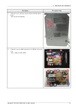
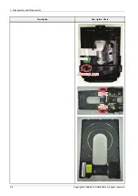
7.

Pull the Jack.

Lift BT Module.


8.

Unfasten 14 screws, and then separate the Front PCB from Front
Panel.
: BH,+,-,B,M3,L10,ZPC(WHT)

3-6

Copyright© 1995-2013 SAMSUNG. All rights reserved.

Summary of Contents for MX-J730

Page 1: ...730 XA SERVICEMANUAL MINI Compact System MX J730 Contents 1 Precaution 2 Product Specification 3 Disassembly and Reassembly 4 Troubleshooting 5 PCB Diagram 6 Schematic Diagram Refer to the service manual in the GSPN see the rear cover for more information ...

Page 2: ...r 4 2 4 1 2 No Output 4 4 4 2 Measures to be taken when the Protection Circuit operates 4 5 4 2 1 Operation of Power Block Protection Circuit 4 5 4 2 2 Check AMP in Power Protection 4 6 4 3 MICOM MPEG Initialization Update 4 7 4 4 Buyer Region Code Setting Method 4 8 4 4 1 The inserting method of Region Code after replacing the Main PBA 4 8 5 PCB Diagram 5 1 5 1 Wiring Diagram 5 1 5 2 FRONT PCB To...

Page 3: ...RONT 1 6 2 6 3 FRONT 2 6 3 6 4 FRONT 3 6 4 6 5 MAIN 1 6 5 6 6 MAIN 2 6 6 6 7 MAIN 3 6 7 6 8 MAIN 4 6 8 6 8 1 Test Point Wave Form 6 9 6 9 MAIN 5 6 10 6 10 SMPS 6 11 Copyright 1995 2013 SAMSUNG All rights reserved ii ...

Page 4: ...hanical or electrical design of the unit Example Do not add auxiliary audio or video connectors Such alterations might create a safety hazard Also any design changes or additions will void the manufacturer s warranty 4 Leakage Current Hot Check Figure 1 1 AC Leakage Test WARNING Do not use an isolation transformer during this test Use a leakage current tester or a metering system that complies Wit...

Page 5: ... 7 Observe the original lead dress especially near the following areas Antenna wiring sharp edges and especially the AC and high voltage power supplies Always inspect for pinched out of place or frayed wiring Do not change the spacing between components and the printed circuit board Check the AC power cord for damage Make sure that no wires or components touch thermally hot parts 8 Product Safety ...

Page 6: ...nsulation between the blades of the AC plug and accessible conductive parts examples metal panels input terminals and earphone jacks 6 Insulation Checking Procedure Disconnect the power cord from the AC source Connect an insulation resistance meter 500 V to the blades of the AC plug The insulation resistance between each blade of the AC plug and accessible conductive parts see above should be grea...

Page 7: ... not use freon propelled chemicals These can generate electrical charges that damage ESDs 4 Use only a grounded tip soldering iron when soldering or unsoldering ESDs 5 Use only an anti static solder removal device Many solder removal devices are not rated as anti static these can accumulate sufficient electrical charge to damage ESDs 6 Do not remove a replacement ESD from its protective package un...

Page 8: ...ct Special places a place where a large amount of dust is accumulated where chemical substances are used or the ambient temperature is too high or low a place that is full of moisture or water in transportation vehicles such as a car or in public places such as the airport or subway station where the product is supposed to operate uninterruptedly for a long time 6 Keep the packaging plastic wrappe...

Page 9: ...2015 CD Ripping Able to ripping while listening GIGA Mode Demo Demo Music Play Football Mode Non Stop Music Relay CD USB Program Auto Change Connectivity USB Host Twin USB TV Sound Connect Bluetooth BT Power On Disc Type 1 Tray 12 cm CD Compatible CD DA CD R RW WMA MP3 ISO9660 Copyright 1995 2013 SAMSUNG All rights reserved 2 1 ...

Page 10: ...Watts 10 THD Front speaker output 220 W CH 4 Ω 100 Hz MX J730 600 Watts MAX 300 W CH 4 Ω 100 Hz Front speaker output 250 W CH 4 Ω 100 Hz Frequency range 20 Hz 20 KHz S N Ratio 80 dB Channel separation 65 dB Amplifier Input sensitivity AUX 2V NOTE Samsung Electronics Co Ltd reserves the right to change the specifications without notice Weight and dimensions are approximate Design and specifications...

Page 11: ...D RW COMPATIBLE FILE WMA MP3 WMA MP3 WMA MP3 USB HOST 1 0 2 2 1 CD RIPPING O O O BLUETOOTH O O O AUDIO IN RCA O O O MIC IN X X O HEADPHONE OUT X X X VIDEO OUT X X X FM AM O O O O O O SPK IMPEDANCE Front 4 ohm Front 4 ohm Front 4 ohm STBY POWER CONSUMPTION 0 45 W 0 45 W 0 45 W MAIN SIZE mm 200 W X 308 5 H X 230 D 200 W X 308 5 H X 230 D 203 W X 306 H X 256 5 D SPK SIZE mm 232 W X 331 H X 294 D 223 ...

Page 12: ... 2 4 Accessories 2 4 1 Supplied Accessories Accessories Item Item code Batteries AAA 4301 000116 Remote Control AH59 02694B User s Manual AH68 02791D FM Antenna AH42 00021A 2 4 Copyright 1995 2013 SAMSUNG All rights reserved ...

Page 13: ... sure to carefully read and understand the safety instructions before performing any work as the IC chips on the PCB are vulnerable to static electricity In order to assemble reverse the order of disassembly Description Description Photo 1 Unfasten 4 screws on the 2 side Cover BH B M3 L10 ZPC BLK CAUTION Be careful not to make any scratches as you remove them Copyright 1995 2013 SAMSUNG All rights...

Page 14: ...3 Disassembly and Reassembly Description Description Photo 2 Separate the Front Panel 3 2 Copyright 1995 2013 SAMSUNG All rights reserved ...

Page 15: ...n Description Photo 3 Unfasten 2 screws and then separate the Rear PCB from Rear Panel BH B M3 L10 ZPC BLK 4 Unfasten 5 screws in SMPS and detach AC CORD 13P shield wire BH B M3 L10 ZPC WHT Copyright 1995 2013 SAMSUNG All rights reserved 3 3 ...

Page 16: ...3 Disassembly and Reassembly Description Description Photo 5 Unfasten 4 kitting screws and detach DECK wire BH B M3 L10 ZPC WHT 3 4 Copyright 1995 2013 SAMSUNG All rights reserved ...

Page 17: ...3 Disassembly and Reassembly Description Description Photo 6 Unfasten 2 screws from inside separate DECK from mecha BH B M3 L10 ZPC BLK Copyright 1995 2013 SAMSUNG All rights reserved 3 5 ...

Page 18: ...nd Reassembly Description Description Photo 7 Pull the Jack Lift BT Module 8 Unfasten 14 screws and then separate the Front PCB from Front Panel BH B M3 L10 ZPC WHT 3 6 Copyright 1995 2013 SAMSUNG All rights reserved ...

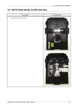
Page 19: ...3 Disassembly and Reassembly 3 2 DECK Disassembly and Reassembly Description Description Photo 1 Separate Tray Disc from DECK Copyright 1995 2013 SAMSUNG All rights reserved 3 7 ...

Page 20: ...3 Disassembly and Reassembly Description Description Photo 3 8 Copyright 1995 2013 SAMSUNG All rights reserved ...

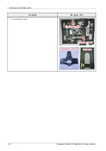
Page 21: ...3 Disassembly and Reassembly Description Description Photo 2 Lift up Holder Cable separate Traverse DECK Copyright 1995 2013 SAMSUNG All rights reserved 3 9 ...

Page 22: ...3 Disassembly and Reassembly Description Description Photo 3 Disassemble complete 3 10 Copyright 1995 2013 SAMSUNG All rights reserved ...

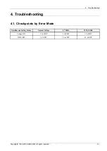
Page 23: ...ooting 4 1 Checkpoints by Error Mode Oscilloscope Setting Values Normal Voltage 27 MHz 32 768 KHz Voltage DIV 1 Vol DIV 1 Vol DIV 1 Vol DIV TIME DIV 1 uS DIV 10 ns DIV 0 1 uS DIV Copyright 1995 2013 SAMSUNG All rights reserved 4 1 ...

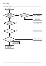
Page 24: ...4 Troubleshooting 4 1 1 No Power 4 2 Copyright 1995 2013 SAMSUNG All rights reserved ...

Page 25: ...4 Troubleshooting Copyright 1995 2013 SAMSUNG All rights reserved 4 3 ...

Page 26: ...4 Troubleshooting 4 1 2 No Output 4 4 Copyright 1995 2013 SAMSUNG All rights reserved ...

Page 27: ...is over current at the AMP IC Speaker Wire Short 2 If temperature of the AMP IC is over 150 3 There is no power supply for amp Protection Circuit operates when power problem occurs in the SMPS Protection Location Pin No Open Short Remark 5 3 V 5 X X PVDD 33 V 15 16 X X 5 V 9 X X MX J730 SMPS PCB CN851 P ON 5 3 V 1 X X Copyright 1995 2013 SAMSUNG All rights reserved 4 5 ...

Page 28: ... can check the PCB without disassembling the set CAUTION Do not connect the power cord during the test Measurement Resistance using Tester R CH 2 kΩ L CH 2 kΩ If Measured Resistance is very different from above numbers There is a Problem AMP Part Problem 4 6 Copyright 1995 2013 SAMSUNG All rights reserved ...

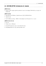
Page 29: ...e 1 Prepare Rom file at USB Memory Update file name MX J730WWB XXXX rom 2 Update file name 3 Insert USB Memory and play UPDATE will be displayed Set will be power off on open MPEG Version Check 1 Power On 2 CD mode select OPEN status 3 Push the button for 5 seconds check the MICOM version 4 Push the button for 5 seconds check the MPEG version Copyright 1995 2013 SAMSUNG All rights reserved 4 7 ...

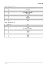
Page 30: ...not working properly if you don t insert the region code The region code is inserted by the remote control 1 Change to AUX function and then push the ENTER button about 10 second 2 When displayed TEST input 46 to set the buyer 3 When displayed input the buyer code refer to the follow Option Table 4 It will show the buyer that you set up Then the buyer setting is succeed 4 8 Copyright 1995 2013 SAM...

Page 31: ...nesia Asia Hongkong 03 USA Canada 04 Iran HC 05 Europe 06 Philippines 07 KOR 08 KOR Table 4 2 MX J650 Option Table Region Code Buyer 20 Latin American 21 Brazil 22 Africa Indonesia Asia Hongkong 23 USA Canada 24 Iran HC 25 Europe 26 Philippines 27 KOR 27 KOR Copyright 1995 2013 SAMSUNG All rights reserved 4 9 ...

Page 32: ...5 PCB Diagram 5 PCB Diagram 5 1 Wiring Diagram 5 1 Copyright 1995 2013 SAMSUNG All rights reserved ...

Page 33: ...5 PCB Diagram 5 2 FRONT PCB Top Copyright 1995 2013 SAMSUNG All rights reserved 5 2 ...

Page 34: ... VFD 4 VFD 5 DGND 6 VFD_CE 7 VFD_CLK 8 VFD_DO 9 KEY3 10 RE_IN 11 ST_5V 12 ST_5V 13 DGND 3 CN1 Connect to Main Pin No Signal 1 VP 2 VFD 3 VFD 4 DGND 5 VFD_CE 6 VFD_CLK 7 VFD_DO 8 JOG 9 JOG 10 DGND 11 KEY_AD2 12 KEY_AD1 13 DGND 14 REMOTE 15 ST_5 1V 16 USB1_5V 17 USB1_DN 18 USB1_DN 19 USB1_DP 20 USB1_DP 21 USB2_5V 22 GND 23 USB2_DN 24 USB2_DN 25 USB2_DP 26 USB2_DP 27 DGND 5 3 Copyright 1995 2013 SAMS...

Page 35: ...5 PCB Diagram 5 3 FRONT PCB Bottom Copyright 1995 2013 SAMSUNG All rights reserved 5 4 ...

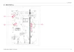
Page 36: ...5 PCB Diagram 5 4 MAIN PCB Top 5 5 Copyright 1995 2013 SAMSUNG All rights reserved ...

Page 37: ...ontrol Pin No Signal 1 SP 2 SP 3 SL 4 SL 5 INSW 6 OUTSW 7 GND 8 NC 9 NC 4 UCN1 FRONT Panel Control Pin No Signal 1 VH 2 VFD 3 VFD 4 DGND 5 VFD_CE 6 VFD_CLK 7 VFD_DO 8 JOG 9 JOG 10 KEY_AD2 11 KEY_AD1 12 DGND 13 REMOCON 14 5 1V 15 USB1_5 2V 16 5 1V 17 USB1_DN 18 USB1_DN 19 USB1_DP 20 USB1_DP 21 USB2_5 2V 22 DGND 23 USB2_DN 24 USB2_DN 25 USB2_DP 26 USB2_DP 27 DGND 5 PCN2 VFD CD Voltage Supply Pin No ...

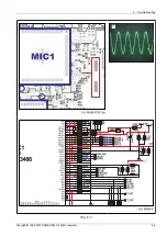
Page 38: ...5 PCB Diagram 5 4 2 Test Point Wave Form TP1 5 7 Copyright 1995 2013 SAMSUNG All rights reserved ...

Page 39: ...5 PCB Diagram 5 5 MAIN PCB Bottom Copyright 1995 2013 SAMSUNG All rights reserved 5 8 ...

Page 40: ...5 PCB Diagram 5 6 SMPS PCB Top 5 9 Copyright 1995 2013 SAMSUNG All rights reserved ...

Page 41: ...Connection 1 CN851 VFD CD AMP Voltage Supply Pin No Signal 1 VFD 2 P ON 3 VFD 4 DGND 5 VH 6 A5 3V 7 DGND 8 DGND 9 VPS 10 A 5V 11 PVDD 12 PVDD 13 AGND 14 AGND 15 PVDD 16 PVDD Copyright 1995 2013 SAMSUNG All rights reserved 5 10 ...

Page 42: ...5 PCB Diagram 5 7 SMPS PCB Bottom 5 11 Copyright 1995 2013 SAMSUNG All rights reserved ...

Page 43: ...n this PCB Audio signal comes from CD DECK USB TUNER AUX Bluetooth and so on decoded by MPEG IC and then transfer to AMP IC The signal is sent to the Crystal amplificatory circuit through MPEG IC This Crystal amplificatory circuit is Low Pass Filtered Sound will be hear by Connecting the Speaker system Copyright 1995 2013 SAMSUNG All rights reserved 6 1 ...

Page 44: ...6 Schematic Diagram 6 2 FRONT 1 6 2 Copyright 1995 2013 SAMSUNG All rights reserved ...

Page 45: ...6 Schematic Diagram 6 3 FRONT 2 Copyright 1995 2013 SAMSUNG All rights reserved 6 3 ...

Page 46: ...6 Schematic Diagram 6 4 FRONT 3 6 4 Copyright 1995 2013 SAMSUNG All rights reserved ...

Page 47: ...6 Schematic Diagram 6 5 MAIN 1 Copyright 1995 2013 SAMSUNG All rights reserved 6 5 ...

Page 48: ...6 Schematic Diagram 6 6 MAIN 2 6 6 Copyright 1995 2013 SAMSUNG All rights reserved ...

Page 49: ...6 Schematic Diagram 6 7 MAIN 3 Copyright 1995 2013 SAMSUNG All rights reserved 6 7 ...

Page 50: ...6 Schematic Diagram 6 8 MAIN 4 6 8 Copyright 1995 2013 SAMSUNG All rights reserved ...

Page 51: ...6 Schematic Diagram 6 8 1 Test Point Wave Form TP1 Copyright 1995 2013 SAMSUNG All rights reserved 6 9 ...

Page 52: ...6 Schematic Diagram 6 9 MAIN 5 6 10 Copyright 1995 2013 SAMSUNG All rights reserved ...

Page 53: ...6 Schematic Diagram 6 10 SMPS Copyright 1995 2013 SAMSUNG All rights reserved 6 11 ...

Page 54: ...na Japan https gspn2 samsungcsportal com N America S America https gspn3 samsungcsportal com This Service Manual is a property of Samsung Electronics Co Ltd Any unauthorized use of Manual can be punished under applicable International and or domestic law 2013 Samsung Electronics Co Ltd All rights reserved Printed in Korea ...

Reviews: